EP0457542B1 - Transceiver with Doppler correction - Google Patents
Transceiver with Doppler correction Download PDFInfo
- Publication number
- EP0457542B1 EP0457542B1 EP91304299A EP91304299A EP0457542B1 EP 0457542 B1 EP0457542 B1 EP 0457542B1 EP 91304299 A EP91304299 A EP 91304299A EP 91304299 A EP91304299 A EP 91304299A EP 0457542 B1 EP0457542 B1 EP 0457542B1
- Authority
- EP
- European Patent Office
- Prior art keywords
- carrier frequency
- signal
- transmitting
- frequency
- receiving
- Prior art date
- Legal status (The legal status is an assumption and is not a legal conclusion. Google has not performed a legal analysis and makes no representation as to the accuracy of the status listed.)
- Expired - Lifetime
Links
Images
Classifications
-
- H—ELECTRICITY
- H04—ELECTRIC COMMUNICATION TECHNIQUE
- H04B—TRANSMISSION
- H04B7/00—Radio transmission systems, i.e. using radiation field
- H04B7/24—Radio transmission systems, i.e. using radiation field for communication between two or more posts
- H04B7/26—Radio transmission systems, i.e. using radiation field for communication between two or more posts at least one of which is mobile
-
- H—ELECTRICITY
- H04—ELECTRIC COMMUNICATION TECHNIQUE
- H04L—TRANSMISSION OF DIGITAL INFORMATION, e.g. TELEGRAPHIC COMMUNICATION
- H04L27/00—Modulated-carrier systems
- H04L27/18—Phase-modulated carrier systems, i.e. using phase-shift keying
- H04L27/22—Demodulator circuits; Receiver circuits
Definitions
- This invention relates to apparatus for and methods of transmitting a signal responsive to a received signal.
- TDMA time division multiple access
- a base station and a mobile station communicate via radio waves.
- six receiving slots are provided for every channel of the 900 MHz band, and in each mobile station an incoming signal in one of the six slots is received for a period of 20 milliseconds at intervals of 120 milliseconds.
- Six transmission slots are similarly provided for every channel, and in each mobile station an outgoing signal in one of the six transmission slots is similarly transmitted.
- a reference receiving carrier frequency and a reference transmitting carrier frequency in a single mobile station are different from each other. By way of example, a frequency 45 MHz lower than the reference receiving carrier frequency is employed as the reference transmitting carrier frequency.
- an offset frequency occurs in the actual received carrier frequency due to the Doppler effect. Also, if the oscillation frequency of a reference oscillator in the base station, which uses a quartz crystal, is not correct, then another offset frequency will occur. In the mobile station, the offset frequency of the transmitted carrier frequency must be maintained within a band ⁇ 200 Hz from the reference transmitting carrier frequency.
- the mobile station be provided with a phase locked loop (PLL) which is locked to the carrier frequency of the received signal thereby to produce the transmitting carrier signal.
- PLL phase locked loop
- the received signal is a burst signal which is received for 20 milliseconds at intervals of 120 milliseconds
- the lock frequency must be determined during a short period of time (20 milliseconds) and maintained for a period of 100 milliseconds between received signals, and the transmission offset frequency must be maintained within the band ⁇ 200 Hz from the reference transmitting carrier frequency.
- US-A-4 489 413 discloses a transmitting and receiving apparatus for transmitting a signal at a transmitted carrier frequency and receiving a signal at a received carrier frequency
- a transmitting and receiving apparatus for receiving a signal of an actual received carrier frequency and transmitting a signal of an actual transmitted carrier frequency, the apparatus comprising:
- a method of transmitting a signal of an actual transmitted carrier frequency which follows the actual received carrier frequency of a received signal comprising:
- embodiments of the present invention can provide a communication system in which an outgoing signal has a transmission offset frequency which follows a reception offset frequency, so that the actual transmitted carrier frequency of the outgoing signal follows the actual received carrier frequency of the received signal and can be transmitted with satisfactory responsiveness and ease.
- Figure 1 shows an embodiment of transmitting and receiving system applied to a TDMA digital communication system in which the base station and the mobile station communicate via radio waves.
- Six receiving slots for example, are provided for every channel of the 900 MHz band, and a mobile station receives an incoming signal in one slot thereof at intervals of 120 milliseconds for a period of 20 milliseconds.
- Six transmission slots are similarly provided for every channel, and a mobile station transmits an outgoing signal in one slot thereof with a similar time and interval.
- the reference receiving carrier frequency and the reference transmitting carrier frequency in any given mobile station are different from each other.
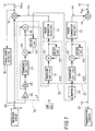
- FIG. 1 shows how the signal processing occurs with a digital signal processor in a mobile station, such as a mobile telephone.
- a signal RX received by a receiving circuit 11 is supplied through a multiplier 12 to a phase error detector 10.
- the phase error detector 10 produces only the imaginary part of the signal supplied thereto.
- the output of the phase error detector 10 is supplied to a loop filter (LF) 14 of a phase locked loop (PLL) 13.
- LF loop filter
- PLL phase locked loop
- the PLL 13 comprises a PLL 13R and a PLL 13T.
- the PLL 13R comprises the loop filter 14, a voltage controlled oscillator (VCO) 15 and a phase converter [exp(j ⁇ ] 16.
- the PLL 13T similarly comprises the loop filter 14, a VCO 21 and a phase converter [exp(j ⁇ ] 22.
- the phase converters 16 and 22 generate complex sine waves corresponding to the signals supplied thereto.
- the sampling circuit 27, the adder 28 and the delay circuit 29 form an integrator.
- the VCO 15 comprises a sampling circuit 31 for sampling the output of the loop filter 14, that is, the output of the adder 30, again at a sampling interval Ts, an adder 32 for adding the output of the sampling circuit 31 and the output of a delay circuit 33, and the delay circuit 31, which again delays the output of the adder 32 by one sampling interval Ts and supplies the resulting delayed signal back to the adder 32.
- the VCO 15 also forms an integrator.
- the output of the VCO 15, that is, the output of the adder 32, is then supplied to the phase converter 16, in which the phase thereof is determined.
- the output of the phase converter 16 is supplied to the multiplier 12.
- the VCO 21 is supplied with a signal from the loop filter 14, that is, the output of the adder 28, through a buffer 20, and comprises a sampling circuit 34, again having a sampling interval Ts, an adder 35 for adding the output of the sampling circuit 34 and the output of a delay circuit 36, and the delay circuit 36 which again delays the output of the adder 35 by one sampling interval Ts and supplies the resulting delayed signal back to the adder 35, thus again forming an integrator.
- the VCO 21 may alternatively be supplied with the output of the loop filter 14, that is, the output of the adder 30, through the buffer 20.
- the output of the VCO 21, that is, the output of the adder 35, is then supplied to the phase converter 22, in which the phase thereof is determined, and the output of the phase converter 22 is fed to a multiplier 19.
- FR RF o ⁇ ⁇ F
- RF o the reference receiving carrier frequency
- ⁇ F the offset frequency
- the signal RX obtained from the receiving circuit 11 is supplied through the multiplier 12 and the phase error detector 10 to the loop filter 14, in which an angular frequency ⁇ of the offset frequency ⁇ F is detected, and this detected angular frequency ⁇ is supplied to the VCO 15, in which the angle ⁇ is detected.
- the angle ⁇ is then supplied to the phase converter 16, which then generates a frequency signal x R of the offset frequency ⁇ F, and this frequency signal x R is supplied to the multiplier 12, where it is multiplied with the received signal RX, so that a received signal RX o , having the reference receiving carrier frequency FR o , is obtained at the output terminal 17.
- This received signal RX o is supplied to, and demodulated by, a demodulator (not shown) to provide an audio signal.
- Another angular frequency ⁇ ' (the output of the adder 28) of an offset frequency ⁇ F' detected by the integrator formed of the elements 27, 28 and 29 within the loop filter 14 is supplied to the VCO 21, and an angle ⁇ ' is detected.
- This detected angle ⁇ ' is supplied to the phase converter 22 which generates a frequency signal x T of the offset frequency ⁇ F'.
- This frequency x T is supplied to multiplier 19, where it is multiplied with a transmission signal TX o , supplied from a terminal 18 and having a reference transmission carrier frequency FT o , to provide a transmission signal TX having an actual transmission carrier frequency FT.
- This transmission signal TX is transmitted to the base station from a transmitter 23.
- FT FT o ⁇ ⁇ F'
- FT o the reference transmitting carrier frequency
- the angular frequency ⁇ supplied to the VCO 15 must follow the received signal and must thus be the output of the adder 30.
- the angular frequency ⁇ ' supplied to the VCO 21 need not follow the received signal so that the signal-to-noise (S/N) ratio can be improved by utilizing the output of the adder 28, which has the low noise of the received signal, before additional noise is added by the adder 30.
- the difference between the angular frequencies ⁇ and ⁇ ' is negligible in comparison with the difference between the transmission and reception frequencies.
- the transmission signal TX has an actual transmitted carrier frequency FT with the same transmission offset frequency ⁇ F' as the reception offset frequency ⁇ F', and can easily be transmitted with excellent responsiveness.
- the offset frequency ⁇ F of the actual received carrier frequency FR of the received signal RX relative to the reference receiving carrier frequency FR o is detected by the PLL 13R and the frequency signal x R of the thus detected offset frequency ⁇ F is provided and then multiplied by the transmission signal RX of the actual received carrier frequency FR by the multiplier 12 to produce the reception signal RX o of the reference receiving carrier frequency FR o .
- the audio signal can be demodulated with the same demodulation characteristics as that of a reception signal RX o of the reference received carrier frequency FR o by the demodulating circuit.
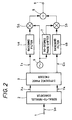
- This embodiment uses a ⁇ /4 shifted quadrature phase shift keying (QPSK) modulation circuit which is shown in Figure 2.
- QPSK quadrature phase shift keying
- the invention is not limited to such a modulating circuit, and can be applied to an analogue or a digital communication system.
- a serial digital audio signal bm from an input terminal 1 is supplied to a serial-to-parallel converter 2, where it is converted to parallel digital signals X K and Y K of two bits and then supplied to a differential phase encoder 3.
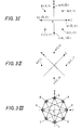
- points A (1, 1), B (-1, 1), C (-1, -1) and D (1, -1) on the perpendicular I axis (real axis and Q axis (imaginary axis) are determined.
- points a (1, 1), b (-1, 1), c (-1, -1) and d (1, -1) on the perpendicular I' axis (real axis) and Q' axis (imaginary axis) which result from rotating the orthogonal I axis and Q axis coordinates by 45 degrees ( ⁇ /4) are also determined.
- the coordinates of the points a, b, c and d on the I' axis and Q' axis coordinates on the I axis and Q axis are presented as a (0, 2 ), b (- 2 , 0), c (0, - 2 ) and d ( 2 , 0).
- the encoded outputs I K and Q K of the encoder 3 are then moved from any one of the points A to D on the I axis and Q axis coordinates to any one of the points a to d in accordance with the outputs X K and Y K of two bits from the serial-to-parallel converter 2 and moved from any one of the points a to d to any one of the points A to D in response to the outputs X K and Y K of two bits of the serial-to-parallel converter 2.
- the movements between any one of the points a to d are represented in Figure 3III. Such moves never pass through the origin 0.
- the encoded outputs I K and Q K are respectively supplied through baseband filters 4 a and 4b to modulators (multipliers) 5a and 5b, where a carrier from a carrier generator 6 and a carrier whose phase is shifted by 90 degrees from the former carrier by a 90 degree phase shifter 7 are modulated (multiplied) with the respective encoded outputs.
- the outputs are then added by an adder 8 and output from an output terminal 9 as a digital modulated signal.
- the reference receiving carrier frequency and the reference transmitting carrier frequency are different.
- An offset frequency which is the difference in the actual received carrier frequency of the received signal relative to the reference received carrier frequency, is detected.
- the frequency signal of the thus detected offset frequency is multiplied by the transmission signal of the reference transmitting carrier frequency to obtain a transmission signal of an actual transmitted carrier frequency which has an offset frequency relative to the reference transmitting carrier frequency which follows the offset frequency of the received signal.
- the transmission signal can then easily be transmitted with satisfactory responsiveness.
Description
- This invention relates to apparatus for and methods of transmitting a signal responsive to a received signal.
- One known type of digital cellular communication system is a time division multiple access (TDMA) system in which a base station and a mobile station communicate via radio waves. In a TDMA system, six receiving slots, for example, are provided for every channel of the 900 MHz band, and in each mobile station an incoming signal in one of the six slots is received for a period of 20 milliseconds at intervals of 120 milliseconds. Six transmission slots are similarly provided for every channel, and in each mobile station an outgoing signal in one of the six transmission slots is similarly transmitted. A reference receiving carrier frequency and a reference transmitting carrier frequency in a single mobile station are different from each other. By way of example, a frequency 45 MHz lower than the reference receiving carrier frequency is employed as the reference transmitting carrier frequency.
- When the mobile station moves, an offset frequency occurs in the actual received carrier frequency due to the Doppler effect. Also, if the oscillation frequency of a reference oscillator in the base station, which uses a quartz crystal, is not correct, then another offset frequency will occur. In the mobile station, the offset frequency of the transmitted carrier frequency must be maintained within a band ±200 Hz from the reference transmitting carrier frequency.
- For this reason, it has been proposed that the mobile station be provided with a phase locked loop (PLL) which is locked to the carrier frequency of the received signal thereby to produce the transmitting carrier signal. However, since the received signal is a burst signal which is received for 20 milliseconds at intervals of 120 milliseconds, it is very difficult to lock the PLL to the carrier frequency of the received signal, as the lock frequency must be determined during a short period of time (20 milliseconds) and maintained for a period of 100 milliseconds between received signals, and the transmission offset frequency must be maintained within the band ±200 Hz from the reference transmitting carrier frequency.
- US-A-4 489 413 discloses a transmitting and receiving apparatus for transmitting a signal at a transmitted carrier frequency and receiving a signal at a received carrier frequency,
- According to the present invention there is provided a transmitting and receiving apparatus for receiving a signal of an actual received carrier frequency and transmitting a signal of an actual transmitted carrier frequency, the apparatus comprising:
- receiving means for receiving a broadcast signal;
- the apparatus being characterised by:
- reference frequency means for providing a reference receiving carrier frequency and a reference transmitting carrier frequency which are different from each other;
- reception offset frequency detecting means for detecting an offset frequency which is the difference between the actual received carrier frequency of the received signal and the reference receiving carrier frequency;
- transmission signal generating means for generating a first transmission signal having the reference transmitting carrier frequency;
- multiplying means for multiplying the first transmission signal by the detected offset frequency to generate a second transmission signal with the actual transmitted carrier frequency; and transmitting means for transmitting the second transmission signal.
- According to the present invention there is also provided a method of transmitting a signal of an actual transmitted carrier frequency which follows the actual received carrier frequency of a received signal, the method comprising:
- receiving a broadcast signal;
- the method being characterised by:
- providing a reference receiving carrier frequency and a reference transmitting carrier frequency which are different from each other;
- detecting an offset frequency which is the difference between the actual received carrier frequency of the received signal and the reference receiving carrier frequency;
- generating a first transmission signal having the reference transmitting carrier frequency;
- multiplying the first transmission signal by the detected offset frequency to generate a second transmission signal with the actual transmitted carrier frequency; and
- transmitting the second transmission signal.
- Thus embodiments of the present invention can provide a communication system in which an outgoing signal has a transmission offset frequency which follows a reception offset frequency, so that the actual transmitted carrier frequency of the outgoing signal follows the actual received carrier frequency of the received signal and can be transmitted with satisfactory responsiveness and ease.
- According to an aspect of the present invention, a transmitting and receiving apparatus for transmitting and receiving signals with a reference receiving carrier frequency which differs from a reference transmitting carrier frequency comprises a reception offset frequency detecting circuit for detecting an offset frequency of a present carrier frequency of a received signal relative to the reference receiving carrier frequency, a multiplier for multiplying a transmission signal of the reference transmitting carrier frequency with a frequency signal of a detected offset frequency, and a transmitting circuit for transmitting an output signal of the multiplier as the signal of a present transmitted carrier frequency.
- The invention will now be described by way of example with reference to the accompanying drawings, throughout which like parts are referred to by like references, and in which:
- Figure 1 is a block diagram of an embodiment of transmitting and receiving apparatus according to the present invention;
- Figure 2 is a block diagram showing a modulating circuit used in the embodiment; and
- Figures 3I to 3III are diagrams showing the encoding operation of the modulating circuit of Figure 2.
- Figure 1 shows an embodiment of transmitting and receiving system applied to a TDMA digital communication system in which the base station and the mobile station communicate via radio waves. Six receiving slots, for example, are provided for every channel of the 900 MHz band, and a mobile station receives an incoming signal in one slot thereof at intervals of 120 milliseconds for a period of 20 milliseconds. Six transmission slots are similarly provided for every channel, and a mobile station transmits an outgoing signal in one slot thereof with a similar time and interval. The reference receiving carrier frequency and the reference transmitting carrier frequency in any given mobile station are different from each other.
- Figure 1 shows how the signal processing occurs with a digital signal processor in a mobile station, such as a mobile telephone. A signal RX received by a
receiving circuit 11 is supplied through amultiplier 12 to aphase error detector 10. Thephase error detector 10 produces only the imaginary part of the signal supplied thereto. The output of thephase error detector 10 is supplied to a loop filter (LF) 14 of a phase locked loop (PLL) 13. - The
PLL 13 comprises aPLL 13R and aPLL 13T. ThePLL 13R comprises theloop filter 14, a voltage controlled oscillator (VCO) 15 and a phase converter [exp(j θ] 16. ThePLL 13T similarly comprises theloop filter 14, aVCO 21 and a phase converter [exp(j θ] 22. Thephase converters - The
loop filter 14 comprises amultiplier 24 for multiplying the received signal by a coefficient K, amultiplier 25 for multiplying an output of themultiplier 24 by a coefficient a (where a=K/2), asampling circuit 27 for sampling the output of themultiplier 25 at a sampling interval Ts, anadder 28 which adds the output of thesampling circuit 27 and the output of adelay circuit 29, anadder 30 for adding the outputs of themultiplier 24 and theadder 28, and thedelay circuit 29, which delays the output of theadder 28 by one sampling interval Ts and supplies the resulting delayed signal back to theadder 28. Thesampling circuit 27, theadder 28 and thedelay circuit 29 form an integrator. - The
VCO 15 comprises asampling circuit 31 for sampling the output of theloop filter 14, that is, the output of theadder 30, again at a sampling interval Ts, anadder 32 for adding the output of thesampling circuit 31 and the output of a delay circuit 33, and thedelay circuit 31, which again delays the output of theadder 32 by one sampling interval Ts and supplies the resulting delayed signal back to theadder 32. Thus, theVCO 15 also forms an integrator. - The output of the
VCO 15, that is, the output of theadder 32, is then supplied to thephase converter 16, in which the phase thereof is determined. The output of thephase converter 16 is supplied to themultiplier 12. - The
VCO 21 is supplied with a signal from theloop filter 14, that is, the output of theadder 28, through abuffer 20, and comprises asampling circuit 34, again having a sampling interval Ts, anadder 35 for adding the output of thesampling circuit 34 and the output of adelay circuit 36, and thedelay circuit 36 which again delays the output of theadder 35 by one sampling interval Ts and supplies the resulting delayed signal back to theadder 35, thus again forming an integrator. - The VCO 21 may alternatively be supplied with the output of the
loop filter 14, that is, the output of theadder 30, through thebuffer 20. - The output of the
VCO 21, that is, the output of theadder 35, is then supplied to thephase converter 22, in which the phase thereof is determined, and the output of thephase converter 22 is fed to amultiplier 19. - Assuming that FR represents the actual received carrier frequency of the received signal RX detected by the receiving circuit 11 (that is, the signal received by the mobile station from the signal transmitted from the base station). then the actual received carrier frequency FR is expressed as:

- The signal RX obtained from the
receiving circuit 11 is supplied through themultiplier 12 and thephase error detector 10 to theloop filter 14, in which an angular frequency ω of the offset frequency Δ F is detected, and this detected angular frequency ω is supplied to theVCO 15, in which the angle θ is detected. The angle θ is then supplied to thephase converter 16, which then generates a frequency signal xR of the offset frequency Δ F, and this frequency signal xR is supplied to themultiplier 12, where it is multiplied with the received signal RX, so that a received signal RXo, having the reference receiving carrier frequency FRo, is obtained at theoutput terminal 17. This received signal RXo is supplied to, and demodulated by, a demodulator (not shown) to provide an audio signal. - Another angular frequency ω' (the output of the adder 28) of an offset frequency Δ F' detected by the integrator formed of the
elements loop filter 14 is supplied to theVCO 21, and an angle θ' is detected. This detected angle θ' is supplied to thephase converter 22 which generates a frequency signal xT of the offset frequency Δ F'. This frequency xT is supplied to multiplier 19, where it is multiplied with a transmission signal TXo, supplied from aterminal 18 and having a reference transmission carrier frequency FTo, to provide a transmission signal TX having an actual transmission carrier frequency FT. This transmission signal TX is transmitted to the base station from atransmitter 23. - Assuming that Ft represents the actual transmitted carrier frequency of the transmission signal TX, then FT is expressed as:

- The angular frequency ω supplied to the
VCO 15 must follow the received signal and must thus be the output of theadder 30. However, the angular frequency ω' supplied to theVCO 21 need not follow the received signal so that the signal-to-noise (S/N) ratio can be improved by utilizing the output of theadder 28, which has the low noise of the received signal, before additional noise is added by theadder 30. The difference between the angular frequencies ω and ω' is negligible in comparison with the difference between the transmission and reception frequencies. - With this communication system, when the reference receiving carrier frequency FRo and the reference transmitting carrier frequency FTo are different, the offset frequency ΔF' of the actual received carrier frequency FR of the received signal RX relative to the reference receiving carrier frequency FRo is detected by the
PLL 13R and the frequency signal xT of the thus detected offset frequency ΔF' is multiplied by the transmission signal TXo, which has the reference transmitting carrier frequency FTo, by themultiplier 19, to produce the transmission signal TX which is transmitted with an actual transmitted carrier frequency FT. Thus, the transmission signal TX has an actual transmitted carrier frequency FT with the same transmission offset frequency ΔF' as the reception offset frequency ΔF', and can easily be transmitted with excellent responsiveness. - Similarly, the offset frequency Δ F of the actual received carrier frequency FR of the received signal RX relative to the reference receiving carrier frequency FRo is detected by the
PLL 13R and the frequency signal xR of the thus detected offset frequency ΔF is provided and then multiplied by the transmission signal RX of the actual received carrier frequency FR by themultiplier 12 to produce the reception signal RXo of the reference receiving carrier frequency FRo. Thus, even when the actual received carrier frequency FR of the reception signal RX contains the offset frequency ΔF, the audio signal can be demodulated with the same demodulation characteristics as that of a reception signal RXo of the reference received carrier frequency FRo by the demodulating circuit. - This embodiment uses a π /4 shifted quadrature phase shift keying (QPSK) modulation circuit which is shown in Figure 2. However, the invention is not limited to such a modulating circuit, and can be applied to an analogue or a digital communication system.
- As shown in Figure 2, a serial digital audio signal bm from an
input terminal 1 is supplied to a serial-to-parallel converter 2, where it is converted to parallel digital signals XK and YK of two bits and then supplied to adifferential phase encoder 3. - The encoding of the
differential phase encoder 3 will be described with reference to Figures 3I to 3III. - As shown in Figure 3I, points A (1, 1), B (-1, 1), C (-1, -1) and D (1, -1) on the perpendicular I axis (real axis and Q axis (imaginary axis) are determined. Then, as shown in Figure 3II, points a (1, 1), b (-1, 1), c (-1, -1) and d (1, -1) on the perpendicular I' axis (real axis) and Q' axis (imaginary axis), which result from rotating the orthogonal I axis and Q axis coordinates by 45 degrees (π/4) are also determined.
- When the I' axis and Q' axis coordinates are moved in parallel and superimposed on the I axis and Q axis coordinates so that their origins coincide with each other, the coordinates of the points a, b, c and d on the I' axis and Q' axis coordinates on the I axis and Q axis are presented as a (0,


- The encoded outputs IK and QK of the
encoder 3 are then moved from any one of the points A to D on the I axis and Q axis coordinates to any one of the points a to d in accordance with the outputs XK and YK of two bits from the serial-to-parallel converter 2 and moved from any one of the points a to d to any one of the points A to D in response to the outputs XK and YK of two bits of the serial-to-parallel converter 2. The movements between any one of the points a to d are represented in Figure 3III. Such moves never pass through theorigin 0. - The movements between any one of the points A to D on the I axis and Q axis coordinates and any one of the points a to d on the I' axis and Q' axis coordinates can be expressed by the change ΔΦ of the angles of straight lines connecting the respective points and the
origin 0. - Accordingly, the relation between the outputs XK, YK and the difference ΔΦ will be as represented in the following truth table.
XK YK ΔΦ 1 1 -3π/4 0 0 3π/4 0 0 π/4 1 0 -π/4 - The encoded outputs IK and QK are respectively supplied through
baseband filters carrier generator 6 and a carrier whose phase is shifted by 90 degrees from the former carrier by a 90 degree phase shifter 7 are modulated (multiplied) with the respective encoded outputs. The outputs are then added by anadder 8 and output from an output terminal 9 as a digital modulated signal. - Thus, in the embodiment described above, the reference receiving carrier frequency and the reference transmitting carrier frequency are different. An offset frequency, which is the difference in the actual received carrier frequency of the received signal relative to the reference received carrier frequency, is detected. The frequency signal of the thus detected offset frequency is multiplied by the transmission signal of the reference transmitting carrier frequency to obtain a transmission signal of an actual transmitted carrier frequency which has an offset frequency relative to the reference transmitting carrier frequency which follows the offset frequency of the received signal. The transmission signal can then easily be transmitted with satisfactory responsiveness.
Claims (12)
- A transmitting and receiving apparatus for receiving a signal of an actual received carrier frequency and transmitting a signal of an actual transmitted carrier frequency, the apparatus comprising:
receiving means (11) for receiving a broadcast signal;
the apparatus being characterised by:reference frequency means (15, 21) for providing a reference receiving carrier frequency and a reference transmitting carrier frequency which are different from each other;reception offset frequency detecting means (12, 10, 14) for detecting an offset frequency which is the difference between the actual received carrier frequency of the received signal and the reference receiving carrier frequency;transmission signal generating means (18; 1 to 9) for generating a first transmission signal having the reference transmitting carrier frequency;multiplying means (19) for multiplying the first transmission signal by the detected offset frequency to generate a second transmission signal with the actual transmitted carrier frequency; andtransmitting means (23) for transmitting the second transmission signal. - Apparatus according to claim 1 wherein the reference frequency means (15, 21) comprises means for setting the reference receiving carrier frequency and the reference transmitting carrier frequency in a predetermined relationship.
- Apparatus according to claim 1 or claim 2 wherein the receiving means (11) further comprises means for receiving a broadcast signal on a time-division basis, and the transmitting means further comprises means for transmitting the second transmission signal on a time-division basis.
- Apparatus according to claim 1, claim 2 or claim 3 wherein the reception offset frequency detecting means (12, 10, 14) comprises a loop filter (14).
- Apparatus according to claim 4 wherein the loop filter (14) comprises an integrator (27, 28, 29) such that the output signal of the integrator (27, 28, 29) is the reception offset frequency.
- Apparatus according to claim 2 further comprising means for modulating the transmission and received signals by a π/4 shifted quadrature phase shift keying.
- A method of transmitting a signal of an actual transmitted carrier frequency which follows the actual received carrier frequency of a received signal, the method comprising:
receiving (11) a broadcast signal;
the method being characterised by:providing (15,21) a reference receiving carrier frequency and a reference transmitting carrier frequency which are different from each other;detecting (12,10,14) an offset frequency which is the difference between the actual received carrier frequency of the received signal and the reference receiving carrier frequency;generating (18; 1 to 9) a first transmission signal having the reference transmitting carrier frequency;multiplying (19) the first transmission signal by the detected offset frequency to generate a second transmission signal with the actual transmitted carrier frequency; andtransmitting (23) the second transmission signal. - A method according to claim 7 wherein the step of providing (15,21) a reference receiving carrier frequency and a reference transmitting carrier frequency comprises setting the reference receiving carrier frequency and the reference transmitting carrier frequency in a predetermined relationship.
- A method according to claim 7 or claim 8 wherein the step of receiving (11) a broadcast signal further comprises receiving a broadcast signal on a time-division basis, and the step of transmitting the second transmission signal further comprises transmitting the second transmission signal on a time-division basis.
- A method according to claim 7, claim 8 or claim 9 wherein the step of detecting (12,10,14) an offset frequency uses a loop filter (14).
- A method according to claim 10 wherein the loop filter (14) comprises an integrator (27, 28, 29) such that the output signal of the integrator (27, 28, 29) is the reception offset frequency.
- A method according to claim 8 further comprising modulating the transmission and received signals by a π/4 shifted quadrature phase shift keying.
Applications Claiming Priority (2)
| Application Number | Priority Date | Filing Date | Title |
|---|---|---|---|
| JP127585/90 | 1990-05-17 | ||
| JP2127585A JPH0422225A (en) | 1990-05-17 | 1990-05-17 | Communication system |
Publications (3)
| Publication Number | Publication Date |
|---|---|
| EP0457542A2 EP0457542A2 (en) | 1991-11-21 |
| EP0457542A3 EP0457542A3 (en) | 1993-03-03 |
| EP0457542B1 true EP0457542B1 (en) | 1997-09-17 |
Family
ID=14963708
Family Applications (1)
| Application Number | Title | Priority Date | Filing Date |
|---|---|---|---|
| EP91304299A Expired - Lifetime EP0457542B1 (en) | 1990-05-17 | 1991-05-14 | Transceiver with Doppler correction |
Country Status (8)
| Country | Link |
|---|---|
| US (1) | US5261120A (en) |
| EP (1) | EP0457542B1 (en) |
| JP (1) | JPH0422225A (en) |
| KR (1) | KR100210537B1 (en) |
| AU (1) | AU644649B2 (en) |
| CA (1) | CA2042563C (en) |
| DE (1) | DE69127654T2 (en) |
| MY (1) | MY107588A (en) |
Families Citing this family (7)
| Publication number | Priority date | Publication date | Assignee | Title |
|---|---|---|---|---|
| FR2697700B1 (en) * | 1992-11-03 | 1994-12-16 | Alcatel Radiotelephone | Device for correcting a frequency offset due to the Doppler effect in a transmission system. |
| KR100207594B1 (en) * | 1993-03-30 | 1999-07-15 | 윤종용 | Method and apparatus for quadrature phase shift-keying modulation with automatic coding |
| FR2757339B1 (en) * | 1996-12-12 | 1999-01-08 | Alsthom Cge Alcatel | METHOD FOR CORRECTING THE DOPPLER EFFECT IN A RADIOCOMMUNICATION NETWORK WITH MOBILE DEVICES |
| JPH11136180A (en) | 1997-10-31 | 1999-05-21 | Sony Corp | Data communication method, transmitter and cellular radio communication system |
| US6470005B1 (en) * | 1998-12-29 | 2002-10-22 | Thomson Licensing Sa | Transceiver prerotation based on carrier offset |
| WO2002054001A1 (en) * | 2000-12-28 | 2002-07-11 | Showa Denko K.K. | Layered heat exchangers |
| US6920916B2 (en) | 2000-12-28 | 2005-07-26 | Showa Denko K.K. | Layered heat exchangers |
Family Cites Families (13)
| Publication number | Priority date | Publication date | Assignee | Title |
|---|---|---|---|---|
| GB830021A (en) * | 1957-04-02 | 1960-03-09 | Standard Telephones Cables Ltd | Improvements in or relating to radio communication systems |
| US3940695A (en) * | 1974-11-18 | 1976-02-24 | Rca Corporation | Doppler correction of transmission frequencies |
| JPS5197316A (en) * | 1975-02-24 | 1976-08-26 | Eiseitsushinniokeru shuhasudokihoshiki | |
| US4430756A (en) * | 1982-02-22 | 1984-02-07 | General Electric Company | Oscillator control circuit |
| US4489413A (en) * | 1982-07-19 | 1984-12-18 | M/A-Com Dcc, Inc. | Apparatus for controlling the receive and transmit frequency of a transceiver |
| AU571302B2 (en) * | 1983-12-22 | 1988-04-14 | Griffith University | A phase shift keying and phase modulation transmission system |
| US4901368A (en) * | 1987-10-19 | 1990-02-13 | American Telephone And Telegraph Company | Frequency translation correction scheme for satellite communication system |
| JPH021675A (en) * | 1987-12-24 | 1990-01-05 | Nec Corp | Carrier recovering circuit for offset qpsk system |
| CA1288878C (en) * | 1988-08-15 | 1991-09-10 | John D. Mcnicol | Timing and carrier recovery in tdma without preamable sequence |
| GB2232852B (en) * | 1989-05-31 | 1993-10-27 | Technophone Ltd | Offset correction |
| JPH07105822B2 (en) * | 1989-08-10 | 1995-11-13 | 三菱電機株式会社 | Automatic frequency controller |
| WO1991005410A1 (en) * | 1989-09-27 | 1991-04-18 | Motorola, Inc. | Method and apparatus for adjusting the frequency of a two-way radio |
| US5113416A (en) * | 1990-10-26 | 1992-05-12 | Ericsson Ge Mobile Communications Holding, Inc. | Digital radio frequency compensation |
-
1990
- 1990-05-17 JP JP2127585A patent/JPH0422225A/en active Pending
-
1991
- 1991-05-10 US US07/698,660 patent/US5261120A/en not_active Expired - Fee Related
- 1991-05-13 AU AU76473/91A patent/AU644649B2/en not_active Ceased
- 1991-05-14 CA CA002042563A patent/CA2042563C/en not_active Expired - Fee Related
- 1991-05-14 EP EP91304299A patent/EP0457542B1/en not_active Expired - Lifetime
- 1991-05-14 DE DE69127654T patent/DE69127654T2/en not_active Expired - Fee Related
- 1991-05-15 KR KR1019910007817A patent/KR100210537B1/en not_active IP Right Cessation
- 1991-05-15 MY MYPI91000815A patent/MY107588A/en unknown
Also Published As
| Publication number | Publication date |
|---|---|
| US5261120A (en) | 1993-11-09 |
| EP0457542A3 (en) | 1993-03-03 |
| CA2042563C (en) | 2002-07-23 |
| EP0457542A2 (en) | 1991-11-21 |
| DE69127654D1 (en) | 1997-10-23 |
| KR100210537B1 (en) | 1999-07-15 |
| KR910021060A (en) | 1991-12-20 |
| AU644649B2 (en) | 1993-12-16 |
| CA2042563A1 (en) | 1991-11-18 |
| JPH0422225A (en) | 1992-01-27 |
| MY107588A (en) | 1996-04-30 |
| DE69127654T2 (en) | 1998-02-12 |
| AU7647391A (en) | 1991-11-21 |
Similar Documents
| Publication | Publication Date | Title |
|---|---|---|
| CA2071869C (en) | Carrier recovery method and apparatus having an adjustable response time determined by carrier signal parameters | |
| EP0804833B1 (en) | Frequency synchronized bidirectional radio system | |
| US6483880B2 (en) | Radio equipment and peripheral apparatus | |
| US4789993A (en) | One frequency repeater for a digital radio system | |
| US5610946A (en) | Radio communication apparatus | |
| CA1303691C (en) | Carrier recovery phase-locked loop | |
| WO1996019875A9 (en) | Frequency synchronized bidirectional radio system | |
| US5920595A (en) | Inter-cross wave compensation method and apparatus performing frequency conversion on signed not detected by a demodulating unit | |
| CA1238086A (en) | Data transmission using a transparent tone-in band system | |
| EP0457542B1 (en) | Transceiver with Doppler correction | |
| EP0059415B1 (en) | System for demodulation of phase-shift keying signals | |
| JPH0787476B2 (en) | Demodulator | |
| US6861900B2 (en) | Fast timing acquisition for multiple radio terminals | |
| US5497402A (en) | Automatic frequency control device for satellite communications ground system | |
| US5173924A (en) | Method for equalizing received burst signal | |
| JPS6266729A (en) | Same frequency repeating system | |
| JP3018453B2 (en) | Communication method | |
| AU692058C (en) | Frequency synchronized bidirectional radio system | |
| AU742089B2 (en) | Method and apparatus for orthogonal frequency conversion | |
| EP0588884B1 (en) | A method and an apparatus for determining phase and frequency deviation | |
| JPS6277725A (en) | Same frequency relay system | |
| JPS61177054A (en) | Receiving circuit of phase modulating signal | |
| JPH0616613B2 (en) | Polarization multiplexing wireless communication system | |
| JPH0129342B2 (en) | ||
| JPS61159851A (en) | Receiving circuit of phase modulating signal |
Legal Events
| Date | Code | Title | Description |
|---|---|---|---|
| PUAI | Public reference made under article 153(3) epc to a published international application that has entered the european phase |
Free format text: ORIGINAL CODE: 0009012 |
|
| AK | Designated contracting states |
Kind code of ref document: A2 Designated state(s): DE FR GB NL |
|
| PUAL | Search report despatched |
Free format text: ORIGINAL CODE: 0009013 |
|
| AK | Designated contracting states |
Kind code of ref document: A3 Designated state(s): DE FR GB NL |
|
| 17P | Request for examination filed |
Effective date: 19930803 |
|
| 17Q | First examination report despatched |
Effective date: 19960313 |
|
| GRAG | Despatch of communication of intention to grant |
Free format text: ORIGINAL CODE: EPIDOS AGRA |
|
| GRAH | Despatch of communication of intention to grant a patent |
Free format text: ORIGINAL CODE: EPIDOS IGRA |
|
| GRAH | Despatch of communication of intention to grant a patent |
Free format text: ORIGINAL CODE: EPIDOS IGRA |
|
| GRAA | (expected) grant |
Free format text: ORIGINAL CODE: 0009210 |
|
| AK | Designated contracting states |
Kind code of ref document: B1 Designated state(s): DE FR GB NL |
|
| REF | Corresponds to: |
Ref document number: 69127654 Country of ref document: DE Date of ref document: 19971023 |
|
| ET | Fr: translation filed | ||
| PLBE | No opposition filed within time limit |
Free format text: ORIGINAL CODE: 0009261 |
|
| STAA | Information on the status of an ep patent application or granted ep patent |
Free format text: STATUS: NO OPPOSITION FILED WITHIN TIME LIMIT |
|
| 26N | No opposition filed | ||
| REG | Reference to a national code |
Ref country code: GB Ref legal event code: IF02 |
|
| PGFP | Annual fee paid to national office [announced via postgrant information from national office to epo] |
Ref country code: FR Payment date: 20030508 Year of fee payment: 13 |
|
| PGFP | Annual fee paid to national office [announced via postgrant information from national office to epo] |
Ref country code: GB Payment date: 20030514 Year of fee payment: 13 |
|
| PGFP | Annual fee paid to national office [announced via postgrant information from national office to epo] |
Ref country code: DE Payment date: 20030522 Year of fee payment: 13 |
|
| PGFP | Annual fee paid to national office [announced via postgrant information from national office to epo] |
Ref country code: NL Payment date: 20030530 Year of fee payment: 13 |
|
| PG25 | Lapsed in a contracting state [announced via postgrant information from national office to epo] |
Ref country code: GB Free format text: LAPSE BECAUSE OF NON-PAYMENT OF DUE FEES Effective date: 20040514 |
|
| PG25 | Lapsed in a contracting state [announced via postgrant information from national office to epo] |
Ref country code: NL Free format text: LAPSE BECAUSE OF NON-PAYMENT OF DUE FEES Effective date: 20041201 Ref country code: DE Free format text: LAPSE BECAUSE OF NON-PAYMENT OF DUE FEES Effective date: 20041201 |
|
| GBPC | Gb: european patent ceased through non-payment of renewal fee |
Effective date: 20040514 |
|
| PG25 | Lapsed in a contracting state [announced via postgrant information from national office to epo] |
Ref country code: FR Free format text: LAPSE BECAUSE OF NON-PAYMENT OF DUE FEES Effective date: 20050131 |
|
| NLV4 | Nl: lapsed or anulled due to non-payment of the annual fee |
Effective date: 20041201 |
|
| REG | Reference to a national code |
Ref country code: FR Ref legal event code: ST |