EP0450910A2 - Temperature compensation circuit for hall effect element - Google Patents
Temperature compensation circuit for hall effect element Download PDFInfo
- Publication number
- EP0450910A2 EP0450910A2 EP91302871A EP91302871A EP0450910A2 EP 0450910 A2 EP0450910 A2 EP 0450910A2 EP 91302871 A EP91302871 A EP 91302871A EP 91302871 A EP91302871 A EP 91302871A EP 0450910 A2 EP0450910 A2 EP 0450910A2
- Authority
- EP
- European Patent Office
- Prior art keywords
- temperature sensitive
- hall
- resistor
- temperature
- current
- Prior art date
- Legal status (The legal status is an assumption and is not a legal conclusion. Google has not performed a legal analysis and makes no representation as to the accuracy of the status listed.)
- Granted
Links
- 230000005355 Hall effect Effects 0.000 title claims description 19
- 230000035945 sensitivity Effects 0.000 claims abstract description 22
- 239000000463 material Substances 0.000 claims abstract description 9
- 230000001419 dependent effect Effects 0.000 claims abstract description 7
- 239000004065 semiconductor Substances 0.000 claims abstract 3
- 238000000034 method Methods 0.000 claims description 13
- 230000000694 effects Effects 0.000 claims description 4
- 239000000758 substrate Substances 0.000 claims 1
- 238000004519 manufacturing process Methods 0.000 description 5
- 230000007423 decrease Effects 0.000 description 3
- 238000009792 diffusion process Methods 0.000 description 3
- 230000000873 masking effect Effects 0.000 description 3
- 230000008859 change Effects 0.000 description 2
- 230000003247 decreasing effect Effects 0.000 description 2
- 229910019974 CrSi Inorganic materials 0.000 description 1
- 230000001276 controlling effect Effects 0.000 description 1
- 230000006698 induction Effects 0.000 description 1
- 230000004048 modification Effects 0.000 description 1
- 238000012986 modification Methods 0.000 description 1
- 230000008569 process Effects 0.000 description 1
- 230000009467 reduction Effects 0.000 description 1
- 230000001105 regulatory effect Effects 0.000 description 1
- 230000004044 response Effects 0.000 description 1
- 239000010409 thin film Substances 0.000 description 1
- 238000009966 trimming Methods 0.000 description 1
Images


Classifications
-
- G—PHYSICS
- G01—MEASURING; TESTING
- G01D—MEASURING NOT SPECIALLY ADAPTED FOR A SPECIFIC VARIABLE; ARRANGEMENTS FOR MEASURING TWO OR MORE VARIABLES NOT COVERED IN A SINGLE OTHER SUBCLASS; TARIFF METERING APPARATUS; MEASURING OR TESTING NOT OTHERWISE PROVIDED FOR
- G01D3/00—Indicating or recording apparatus with provision for the special purposes referred to in the subgroups
- G01D3/028—Indicating or recording apparatus with provision for the special purposes referred to in the subgroups mitigating undesired influences, e.g. temperature, pressure
- G01D3/036—Indicating or recording apparatus with provision for the special purposes referred to in the subgroups mitigating undesired influences, e.g. temperature, pressure on measuring arrangements themselves
- G01D3/0365—Indicating or recording apparatus with provision for the special purposes referred to in the subgroups mitigating undesired influences, e.g. temperature, pressure on measuring arrangements themselves the undesired influence being measured using a separate sensor, which produces an influence related signal
-
- G—PHYSICS
- G01—MEASURING; TESTING
- G01R—MEASURING ELECTRIC VARIABLES; MEASURING MAGNETIC VARIABLES
- G01R33/00—Arrangements or instruments for measuring magnetic variables
- G01R33/02—Measuring direction or magnitude of magnetic fields or magnetic flux
- G01R33/06—Measuring direction or magnitude of magnetic fields or magnetic flux using galvano-magnetic devices
- G01R33/07—Hall effect devices
-
- Y—GENERAL TAGGING OF NEW TECHNOLOGICAL DEVELOPMENTS; GENERAL TAGGING OF CROSS-SECTIONAL TECHNOLOGIES SPANNING OVER SEVERAL SECTIONS OF THE IPC; TECHNICAL SUBJECTS COVERED BY FORMER USPC CROSS-REFERENCE ART COLLECTIONS [XRACs] AND DIGESTS
- Y10—TECHNICAL SUBJECTS COVERED BY FORMER USPC
- Y10S—TECHNICAL SUBJECTS COVERED BY FORMER USPC CROSS-REFERENCE ART COLLECTIONS [XRACs] AND DIGESTS
- Y10S323/00—Electricity: power supply or regulation systems
- Y10S323/907—Temperature compensation of semiconductor
Definitions
- This invention relates to methods for compensating for the effect of temperature on temperature sensitive electronic devices. More particularly, it relates to methods and circuitry for compensating for the temperature dependence of sensitivity of Hall effect elements and other devices having similar characteristics.
- a Hall effect element is widely used in devices intended for measuring, controlling and regulating purposes.
- a Hall effect element may be used as a stable signal generator or as a switch or boundary value indicator which functions without physical contact.
- a block or sheet of suitable material having orthogonal axes X, Y and Z is fitted with a pair of input electrodes such that a current flows along the X axis and, if a magnetic field is passed through the material generally parallel with the Y axis, then a Hall voltage will be produced across the material in the direction of the Z axis.
- a pair of output electrodes may be connected to the material such that the Hall voltage can be applied to an output circuit.
- Materials suitable for Hall effect devices generally exhibit large increases in resistance with increasing temperature.
- a fixed voltage applied to a Hall or other similar element results in a current therethrough which decreases rapidly with increasing temperature.
- the output voltage of the Hall element decreases.
- This large negative temperature coefficient is manifested as a reduction in sensitivity as temperature increases.
- a large variation in sensitivity cannot be tolerated or is at least undesirable. In such applications it is necessary to provide means for compensating for the temperature dependence.
- British Pat. No. 1,247,955 discloses Hall effect apparatus in which an attempt is made to provide temperature independent sensitivity, in part by maintaining a constant current through a Hall element by connecting large value resistors in series therewith.
- the apparatus also includes an output circuit in which the internal resistance of the Hall element forms part of a feedback network for a differential amplifier.
- the sensitivity of a Hall element can be expressed as: S H - V H B Z - r n qt (N D ) (G T ) (I Y ) wherein:
- the current in the Hall element can be expressed as I Y - V a R H wherein:
- Impedance of the Hall element may be expressed as: wherein:
- a resistor is formed in the same epitaxial layer in which the Hall element is formed. Since this resistor is directly thermally coupled to the Hall element, temperature changes which affect the Hall element also affect this resistor and its resistance will be directly related to temperature sensitivity of the Hall element.
- the voltage across the Hall element is maintained constant and resistance changes in the epitaxial resistor used to control a reference current applied to a load resistor used to measure Hall output.
- the load resistor of course, is temperature sensitive. By allowing the reference voltage across the epitaxial resistor to vary with absolute temperature and inversely proportionally to the load resistor, a temperature dependent voltage directly related to Hall sensitivity is produced. The product of this reference voltage and the resistance of the load resistor thus can be made constant with temperature to produce a temperature independent resistor reference.
- All components of the temperature compensation circuit can be formed on the same chip as the Hall element by conventional integrated circuit diffusion and masking techniques, thus additional costly fabrication steps are avoided. Furthermore, the components of the temperature compensation circuit can be fabricated with trimmable resistors and alternative interconnection arrangements so that the circuit can be selectively arranged to provide constant sensitivity with temperature, increasing sensitivity with increasing temperature, or decreasing sensitivity with increasing temperature. Similarly, configuration options can be included in the circuit fabrication to permit selection of bipolar or unipolar operation.
- FIGURE 1 A diagrammatic representation of a bipolar circuit employing the principles of the invention is shown in FIGURE 1.
- a constant bias voltage which is independent of temperature is supplied to a Hall effect device 10 by a bandgap voltage regulator 11 from an external voltage supply.
- the output of Hall element 10 in response to a magnetic field is amplified by a constant gain amplifier and thus appears,across load resistors RL 1 and RL 2 .
- FIGURE 1 is a bipolar latch circuit which turns on (operates) at a predetermined magnitude and direction of magnetic field and turns off (releases) at the same magnitude but opposite direction of magnetic field.
- a differential transistor switch (not shown) is used to change the comparator threshold polarity and alternately switches transistors Q10 and Q12 on and off to switch a reference current (I ref ) on the collector of Q10 or Q12, respectively, to load resistors RL 1 or RL 2 , respectively.
- the reference current (I ref ) is determined by a current mirror circuit comprising transistors Q1, Q2 and Q3; resistors R1, R2 and R epi and diode D1. It will be recognized that by appropriate selection of the values of resistors R1 and R2, the current (or any function thereof) passing through resistor R epi appears as the current (I ref ) on the collector of transistor Q3.
- the circuit of FIGURE 1 is a bipolar latch circuit designed to operate at a given magnetic threshold irrespective of temperature changes. At the point B op where the magnetic field is sufficient: where:
- resistor R epi is fabricated to the same epitaxial layer in which the Hall element is formed so that the mobility of electrons therein matches the drift mobility of the Hall element.
- the resistance of R epi may be expressed as:
- V ref V ref R epi
- V ref V ref RL
- V ref V ref RL
- R epi constant R epi
- the entire circuit can be formed on the same chip on which the Hall element is formed by relatively simply masking and diffusion techniques. Furthermore, the same masking and diffusion techniques which are used to ordinarily form the amplifier circuit will be used to form the additional components required for the temperature compensation circuit. Thus the effects of temperature change will be canceled and the need for a temperature independent resistor is totally eliminated.
- resistors R1 and R2 can be made selectively variable by conventional trimming techniques.
- the values of resistors R1 and R2 can be selectively adjusted to provide a circuit in which the Hall effect sensitivity can increase with temperature, decrease with temperature, or be maintained relatively constant with temperature changes.
- FIGURE 2 An alternative embodiment of the invention is illustrated in FIGURE 2 wherein the same principles are applied to provide unipolar operation so that the latching circuit turns on (operates) at a predetermined magnitude and direction of magnetic field and turns off (releases) at a predetermined lesser magnitude of the same direction of magnetic field.
- the current I ref on the collector of transistor Q3 is applied directly to load resistor RL 1 .
- transistor Q12 When transistor Q12 is turned on, a fractional portion which is proportional to the desired switching hysteresis is applied to resistor RL 2 .
- the entire circuitry for either unipolar or bipolar operation can be included in the manufacturing process and the desired operational configuration selected by convention interconnection selection techniques.
Landscapes
- Physics & Mathematics (AREA)
- General Physics & Mathematics (AREA)
- Condensed Matter Physics & Semiconductors (AREA)
- Hall/Mr Elements (AREA)
- Measuring Magnetic Variables (AREA)
Abstract
Description
- This invention relates to methods for compensating for the effect of temperature on temperature sensitive electronic devices. More particularly, it relates to methods and circuitry for compensating for the temperature dependence of sensitivity of Hall effect elements and other devices having similar characteristics.
- The Hall effect is widely used in devices intended for measuring, controlling and regulating purposes. For example, in combination with a voltage amplifier, a Hall effect element may be used as a stable signal generator or as a switch or boundary value indicator which functions without physical contact.
- The theory of operation of Hall effect devices is well known. A block or sheet of suitable material having orthogonal axes X, Y and Z is fitted with a pair of input electrodes such that a current flows along the X axis and, if a magnetic field is passed through the material generally parallel with the Y axis, then a Hall voltage will be produced across the material in the direction of the Z axis. A pair of output electrodes may be connected to the material such that the Hall voltage can be applied to an output circuit.
- Materials suitable for Hall effect devices generally exhibit large increases in resistance with increasing temperature. Thus, a fixed voltage applied to a Hall or other similar element results in a current therethrough which decreases rapidly with increasing temperature. As a result of the decreasing current the output voltage of the Hall element decreases. This large negative temperature coefficient is manifested as a reduction in sensitivity as temperature increases. In many applications a large variation in sensitivity cannot be tolerated or is at least undesirable. In such applications it is necessary to provide means for compensating for the temperature dependence.
- A variety of circuits and apparatus have been devised for compensating for the temperature dependent characteristics of a Hall element. For example, British Pat. No. 1,247,955 discloses Hall effect apparatus in which an attempt is made to provide temperature independent sensitivity, in part by maintaining a constant current through a Hall element by connecting large value resistors in series therewith. The apparatus also includes an output circuit in which the internal resistance of the Hall element forms part of a feedback network for a differential amplifier.
- A more practical and widely accepted method for temperature compensation of Hall effect circuits is shown in U.S. Pat. No. 4,521,727 to Atherton, et al. Through use of compensation threshold voltage directly proportional to the current flowing through the Hall element, a magnetic switch point is achieved which is dependent only on the Hall scattering coefficient which has a temperature coefficient of about +700ppm/°C. Key to this method, however, is the use of a resistance element which is temperature independent. Unfortunately, temperature independent resistors such as CrSi thin film resistors must be formed during the circuit fabrication process by process steps not ordinarily employed in manufacturing the Hall element device and associated circuitry. Thus the cost of making such temperature compensated circuits is greatly increased because of the time and expense involved in making the required temperature independent resistor.
- The sensitivity of a Hall element can be expressed as:

- BZ =
- Magnetic induction perpendicular to plane of the sensor
- q =
- Charge on the electron
- ND =
- N-type carrier density in the Hall element
- t =
- Thickness of the Hall element
- VH =
- Hall voltage
- IY =
- Current in the Hall element
- GT =
- Hall element geometry factor
- The current in the Hall element can be expressed as

- Va =
- Voltage across Hall element
- RH =
- Impedance of Hall element.
- Impedance of the Hall element may be expressed as:

wherein: - ρ =
- Resistivity
- L =
- Length
- W =
- Width
- In accordance with the invention, a resistor is formed in the same epitaxial layer in which the Hall element is formed. Since this resistor is directly thermally coupled to the Hall element, temperature changes which affect the Hall element also affect this resistor and its resistance will be directly related to temperature sensitivity of the Hall element. The voltage across the Hall element is maintained constant and resistance changes in the epitaxial resistor used to control a reference current applied to a load resistor used to measure Hall output. The load resistor, of course, is temperature sensitive. By allowing the reference voltage across the epitaxial resistor to vary with absolute temperature and inversely proportionally to the load resistor, a temperature dependent voltage directly related to Hall sensitivity is produced. The product of this reference voltage and the resistance of the load resistor thus can be made constant with temperature to produce a temperature independent resistor reference.
- All components of the temperature compensation circuit can be formed on the same chip as the Hall element by conventional integrated circuit diffusion and masking techniques, thus additional costly fabrication steps are avoided. Furthermore, the components of the temperature compensation circuit can be fabricated with trimmable resistors and alternative interconnection arrangements so that the circuit can be selectively arranged to provide constant sensitivity with temperature, increasing sensitivity with increasing temperature, or decreasing sensitivity with increasing temperature. Similarly, configuration options can be included in the circuit fabrication to permit selection of bipolar or unipolar operation. Other features and advantages of the invention will become more readily understood from the following detailed description taken in connection with the appended claims and attached drawing in which:
-
- FIGURE 1 is a schematic illustration of the preferred embodiment of the invention configured for bipolar operation; and
- FIGURE 2 is a schematic illustration of the preferred embodiment of the invention configured for unipolar operation.
- A diagrammatic representation of a bipolar circuit employing the principles of the invention is shown in FIGURE 1. A constant bias voltage which is independent of temperature is supplied to a
Hall effect device 10 by a bandgap voltage regulator 11 from an external voltage supply. The output ofHall element 10 in response to a magnetic field is amplified by a constant gain amplifier and thus appears,across load resistors RL₁ and RL₂. - The embodiment of FIGURE 1 is a bipolar latch circuit which turns on (operates) at a predetermined magnitude and direction of magnetic field and turns off (releases) at the same magnitude but opposite direction of magnetic field. A differential transistor switch (not shown) is used to change the comparator threshold polarity and alternately switches transistors Q10 and Q12 on and off to switch a reference current (I ref ) on the collector of Q10 or Q12, respectively, to load resistors RL₁ or RL₂, respectively.
- The reference current (I ref ) is determined by a current mirror circuit comprising transistors Q1, Q2 and Q3; resistors R1, R2 and R epi and diode D1. It will be recognized that by appropriate selection of the values of resistors R1 and R2, the current (or any function thereof) passing through resistor R epi appears as the current (I ref ) on the collector of transistor Q3.
- The circuit of FIGURE 1 is a bipolar latch circuit designed to operate at a given magnetic threshold irrespective of temperature changes. At the point B op where the magnetic field is sufficient:

where: - Bop =
- Magnetic field required to operate the circuit
- AV =
- Gain of amplifier
- SH =
- Sensitivity of Hall element.
- In accordance with the invention, resistor R epi is fabricated to the same epitaxial layer in which the Hall element is formed so that the mobility of electrons therein matches the drift mobility of the Hall element. The resistance of R epi may be expressed as:

The current I ref on the collector of transistor Q3 is:
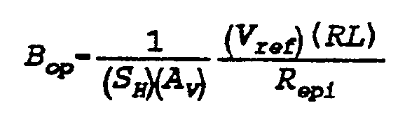
By producing a temperature dependent voltage source V ref which is inversely proportional to the resistance of the load resistor RL, the product of (V ref )(RL) can be made constant with temperature. Thus, with amplifier gain A V constant with temperature:
or
Thus, with V a constant and V ref proportional to V a :
The magnetic threshold, therefore, remains constant with temperature. - It will be observed that the temperature dependence of V ref is equal to the temperature dependence of (1-2K)V BE of transistor Q2 where


- It will be noted that the entire circuit can be formed on the same chip on which the Hall element is formed by relatively simply masking and diffusion techniques. Furthermore, the same masking and diffusion techniques which are used to ordinarily form the amplifier circuit will be used to form the additional components required for the temperature compensation circuit. Thus the effects of temperature change will be canceled and the need for a temperature independent resistor is totally eliminated.
- It will be further noted that the values of resistors R1 and R2 can be made selectively variable by conventional trimming techniques. Thus, the values of resistors R1 and R2 can be selectively adjusted to provide a circuit in which the Hall effect sensitivity can increase with temperature, decrease with temperature, or be maintained relatively constant with temperature changes.
- An alternative embodiment of the invention is illustrated in FIGURE 2 wherein the same principles are applied to provide unipolar operation so that the latching circuit turns on (operates) at a predetermined magnitude and direction of magnetic field and turns off (releases) at a predetermined lesser magnitude of the same direction of magnetic field. In this case the current I ref on the collector of transistor Q3 is applied directly to load resistor RL₁. When transistor Q12 is turned on, a fractional portion

- While the invention has been described with specific reference to compensating for the temperature dependence of Hall element sensitivity, it will be readily recognized that the principles thereof are equally applicable to other devices which are temperature sensitive. Similarly, although the invention is described in detail with reference to specific circuit arrangements, similar effects may be accomplished by use of other circuit arrangements. It is to be understood, therefore, that although the invention has been described with particular reference to specificembodiments thereof, the forms of the invention shown and described in detail are to be taken as preferred embodiments of same, and that various changes and modifications may be resorted to without departing from the spirit and scope of the invention as defined by the appended claims.


Hall sensitivity may be expressed as:

Thus Hall sensitivity is directly proportional to the bias voltage applied to the Hall element and proportional to Hall mobility. Since drift mobility is directly related to Hall mobility, a control element responsive to drift mobility changes with temperature can be used to accurately determine changes in sensitivity under conditions where V a is held constant.
Claims (7)
- A method of compensating for temperature dependent sensitivity in a Hall effect element formed in an epitaxial layer of semiconductor material wherein the output signal of the Hall effect element is detected by measuring the voltage across a temperature sensitive load resistor connected between an output of the Hall effect element and the Hall element bias voltage, the method characterised by the steps of:(a) providing a resistance element in which the electrical resistance varies with temperature sensitivity of the Hall element;(b) using the voltage across said resistance element to provide a voltage source which is inversely proportional to the resistance of the temperature sensitive load resistor; and(c) applying a current proportional to the current through said resistance element to said load resistor.
- A circuit for sensing the effect of a magnetic field on a Hall effect element formed in a layer of epitaxial material, the circuit characterised by:(a) a temperature sensitive load resistor between the Hall element bias voltage and a Hall element output;(b) a temperature sensitive reference resistor providing a temperature sensitive reference voltage which is inversely proportional to the resistance of the temperature sensitive load resistor; and(c) current mirror circuit means providing a current proportional to the current through the reference resistor to the temperature sensitive load resistor so that voltage across the load resistor varies with temperature in direct relationship with the sensitivity of the Hall effect element.
- A circuit according to Claim 2 characterised in that said reference resistor is formed in the same epitaxial layer of material in which the Hall element is formed.
- A circuit according to Claim 2 or 3 characterised by:(d) a second temperature sensitive load resistor between the Hall element bias voltage and a second Hall element output; and(e) means for selectively alternately switching the current proportional to the current through the reference resistor to said temperature sensitive load resistor and said second temperature sensitive load resistor.
- A circuit according to any of Claims 2 to 4 characterised by:(d) a second temperature sensitive load resistor between the Hall element bias voltage and a second Hall element output; and(e) means for selectively switching a current proportional to the current through the reference resistor to said second temperature sensitive load resistor.
- A circuit for providing a temperature compensated output responsive to magnetic field strength the circuit characterised by:(a) a substrate having an epitaxial layer of semiconductor thereon;(b) a temperature sensitive Hall effect element formed in said epitaxial layer having a pair of bias terminals and a pair of output terminals between which a Hall voltage is generated when said Hall effect element is subjected to a magnetic field;(c) power supply means having a first and second terminals operatively connected across said bias terminals;(d) amplifier means operatively connected to said pair of output terminals to receive said Hall voltage, said amplifier means having a first and second output terminals;(e) a first temperature sensitive load resistor connected between said first terminal of said power supply means and said first output terminal of said amplifier means;(f) a second temperature sensitive load resistor connected between said first terminal of said power supply means and said second output terminal of said amplifier means;(g) current mirror circuitry operatively connected between said first and second terminals of said power supply means including a temperature sensitive resistor, the resistance of which is proportional to the temperature sensitivity of said Hall effect element, and a reference output terminal through which the current is proportional to the current through the reference resistor; and(h) switch means operative to selectively alternately connect said reference output terminal to said first and second output terminals of said amplifier means;whereby the voltage across said temperature sensitive load resistors is inversely proportional to the resistance of said temperature sensitive reference resistor.
- A circuit according to Claim 6 characterised in that said temperature sensitive reference resistor is formed in the same epitaxial layer in which the Hall effect element is formed.
Applications Claiming Priority (2)
| Application Number | Priority Date | Filing Date | Title |
|---|---|---|---|
| US07/505,710 US5055768A (en) | 1990-04-05 | 1990-04-05 | Temperature compensator for hall effect circuit |
| US505710 | 1990-04-05 |
Publications (3)
| Publication Number | Publication Date |
|---|---|
| EP0450910A2 true EP0450910A2 (en) | 1991-10-09 |
| EP0450910A3 EP0450910A3 (en) | 1993-03-17 |
| EP0450910B1 EP0450910B1 (en) | 1997-01-08 |
Family
ID=24011502
Family Applications (1)
| Application Number | Title | Priority Date | Filing Date |
|---|---|---|---|
| EP91302871A Expired - Lifetime EP0450910B1 (en) | 1990-04-05 | 1991-04-02 | Temperature compensation circuit for hall effect element |
Country Status (3)
| Country | Link |
|---|---|
| US (1) | US5055768A (en) |
| EP (1) | EP0450910B1 (en) |
| DE (1) | DE69123993T2 (en) |
Cited By (8)
| Publication number | Priority date | Publication date | Assignee | Title |
|---|---|---|---|---|
| WO1994006030A1 (en) * | 1992-09-02 | 1994-03-17 | Santa Barbara Research Center | Magnetoresistive integrated circuit sensor with high output voltage swing and temperature compensation |
| WO1996002849A1 (en) * | 1994-07-19 | 1996-02-01 | Honeywell Inc. | Temperature compensation circuit for a hall effect element |
| EP0701141A3 (en) * | 1994-09-06 | 1997-11-05 | Deutsche ITT Industries GmbH | Magnetic field sensor with Hallelement |
| EP1010987A3 (en) * | 1998-12-19 | 2001-02-14 | Micronas GmbH | Hall sensor |
| DE10032527C1 (en) * | 2000-07-05 | 2001-12-06 | Infineon Technologies Ag | Temperature compensation circuit for Hall element has two band separation reference circuits with resistances of two types, comparator comparing Hall voltage with reference potential |
| WO2002009284A1 (en) * | 2000-07-20 | 2002-01-31 | Honeywell Control Systems Limited | Inductive proximity sensor and related methods |
| EP1096233A3 (en) * | 1999-10-27 | 2006-09-20 | Micronas GmbH | Two wire sensor device |
| IT201700071189A1 (en) * | 2017-06-26 | 2018-12-26 | St Microelectronics Srl | TEMPERATURE COMPENSATION CIRCUIT, CORRESPONDING DEVICE AND PROCEDURE |
Families Citing this family (18)
| Publication number | Priority date | Publication date | Assignee | Title |
|---|---|---|---|---|
| DE59109002D1 (en) * | 1991-07-31 | 1998-07-09 | Micronas Intermetall Gmbh | Hall sensor with self-compensation |
| US5444369A (en) * | 1993-02-18 | 1995-08-22 | Kearney-National, Inc. | Magnetic rotational position sensor with improved output linearity |
| US5455510A (en) * | 1994-03-11 | 1995-10-03 | Honeywell Inc. | Signal comparison circuit with temperature compensation |
| US5488296A (en) * | 1995-01-25 | 1996-01-30 | Honeywell Inc. | Temperature compensated magnetically sensitive circuit |
| US5497084A (en) * | 1995-03-03 | 1996-03-05 | Honeywell Inc. | Geartooth sensor with means for selecting a threshold magnitude as a function of the average and minimum values of a signal of magnetic field strength |
| JPH0968403A (en) * | 1995-08-31 | 1997-03-11 | Denso Corp | Throttle valve opening sensor |
| US5694040A (en) * | 1996-07-02 | 1997-12-02 | Honeywell Inc. | Magnetic sensor circuit with two magnetically sensitive devices |
| US6404188B1 (en) | 1998-03-19 | 2002-06-11 | Honeywell Inc | Single geartooth sensor yielding multiple output pulse trains |
| US6879145B1 (en) | 2002-02-15 | 2005-04-12 | Larry L. Harris | Voltage isolation buffer with hall effect magnetic field sensor |
| US7265539B2 (en) * | 2005-06-09 | 2007-09-04 | Ford Motor Company | Calibration of a hall effect sensor |
| US8421427B2 (en) * | 2007-09-07 | 2013-04-16 | Oki Data Corporation | Reference voltage generation circuit, drive circuit, light emitting diode head, and image forming apparatus |
| US9013167B2 (en) * | 2010-11-09 | 2015-04-21 | Texas Instruments Incorporated | Hall effect device having voltage based biasing for temperature compensation |
| JP5800152B2 (en) * | 2012-10-24 | 2015-10-28 | Tdk株式会社 | Magnetic sensor |
| US9063174B2 (en) | 2012-11-14 | 2015-06-23 | Olympus Scientific Solutions Americas Inc. | Hall effect measurement instrument with temperature compensation |
| CN103825591B (en) * | 2014-03-13 | 2016-08-17 | 北京经纬恒润科技有限公司 | A kind of Hall switch chip |
| JP2017032278A (en) * | 2015-07-28 | 2017-02-09 | エスアイアイ・セミコンダクタ株式会社 | Sensor device |
| US10162017B2 (en) * | 2016-07-12 | 2018-12-25 | Allegro Microsystems, Llc | Systems and methods for reducing high order hall plate sensitivity temperature coefficients |
| US12704563B2 (en) * | 2024-01-23 | 2026-08-11 | Texas Instruments Incorporated | Magnetic gain correction of hall effect sensors |
Family Cites Families (7)
| Publication number | Priority date | Publication date | Assignee | Title |
|---|---|---|---|---|
| US3816766A (en) * | 1973-01-29 | 1974-06-11 | Sprague Electric Co | Integrated circuit with hall cell |
| CA1088159A (en) * | 1977-01-03 | 1980-10-21 | Wilson D. Pace | Hall-effect integrated circuit switch |
| US4521727A (en) * | 1983-05-23 | 1985-06-04 | Honeywell Inc. | Hall effect circuit with temperature compensation |
| US4833406A (en) * | 1986-04-17 | 1989-05-23 | Household Commercial Financial Services Inc. | Temperature compensated Hall-effect sensor apparatus |
| US4734594A (en) * | 1986-12-31 | 1988-03-29 | Honeywell Inc. | Offset correction for sensor with temperature dependent sensitivity |
| US4760285A (en) * | 1987-03-30 | 1988-07-26 | Honeywell Inc. | Hall effect device with epitaxal layer resistive means for providing temperature independent sensitivity |
| US4908527A (en) * | 1988-09-08 | 1990-03-13 | Xolox Corporation | Hall-type transducing device |
-
1990
- 1990-04-05 US US07/505,710 patent/US5055768A/en not_active Expired - Lifetime
-
1991
- 1991-04-02 EP EP91302871A patent/EP0450910B1/en not_active Expired - Lifetime
- 1991-04-02 DE DE69123993T patent/DE69123993T2/en not_active Expired - Fee Related
Cited By (15)
| Publication number | Priority date | Publication date | Assignee | Title |
|---|---|---|---|---|
| WO1994006030A1 (en) * | 1992-09-02 | 1994-03-17 | Santa Barbara Research Center | Magnetoresistive integrated circuit sensor with high output voltage swing and temperature compensation |
| US5402064A (en) * | 1992-09-02 | 1995-03-28 | Santa Barbara Research Center | Magnetoresistive sensor circuit with high output voltage swing and temperature compensation |
| WO1996002849A1 (en) * | 1994-07-19 | 1996-02-01 | Honeywell Inc. | Temperature compensation circuit for a hall effect element |
| US6104231A (en) * | 1994-07-19 | 2000-08-15 | Honeywell International Inc. | Temperature compensation circuit for a hall effect element |
| EP0701141A3 (en) * | 1994-09-06 | 1997-11-05 | Deutsche ITT Industries GmbH | Magnetic field sensor with Hallelement |
| US6362618B1 (en) | 1998-12-19 | 2002-03-26 | Micronas Gmbh | Hall sensor for stress and temperature measurements in addition to magnetic field measurement |
| EP1010987A3 (en) * | 1998-12-19 | 2001-02-14 | Micronas GmbH | Hall sensor |
| EP1096233A3 (en) * | 1999-10-27 | 2006-09-20 | Micronas GmbH | Two wire sensor device |
| DE10032527C1 (en) * | 2000-07-05 | 2001-12-06 | Infineon Technologies Ag | Temperature compensation circuit for Hall element has two band separation reference circuits with resistances of two types, comparator comparing Hall voltage with reference potential |
| WO2002003088A1 (en) * | 2000-07-05 | 2002-01-10 | Infineon Technologies Ag | Temperature compensation circuit for a hall element |
| US6825709B2 (en) | 2000-07-05 | 2004-11-30 | Infineon Technologies Ag | Temperature compensation circuit for a hall element |
| WO2002009284A1 (en) * | 2000-07-20 | 2002-01-31 | Honeywell Control Systems Limited | Inductive proximity sensor and related methods |
| IT201700071189A1 (en) * | 2017-06-26 | 2018-12-26 | St Microelectronics Srl | TEMPERATURE COMPENSATION CIRCUIT, CORRESPONDING DEVICE AND PROCEDURE |
| EP3422032A1 (en) * | 2017-06-26 | 2019-01-02 | STMicroelectronics Srl | A temperature compensation circuit, corresponding device and method |
| US10942228B2 (en) | 2017-06-26 | 2021-03-09 | Stmicroelectronics S.R.L. | Temperature compensation circuit, corresponding device and method |
Also Published As
| Publication number | Publication date |
|---|---|
| EP0450910B1 (en) | 1997-01-08 |
| DE69123993T2 (en) | 1997-07-10 |
| EP0450910A3 (en) | 1993-03-17 |
| DE69123993D1 (en) | 1997-02-20 |
| US5055768A (en) | 1991-10-08 |
Similar Documents
| Publication | Publication Date | Title |
|---|---|---|
| US5055768A (en) | Temperature compensator for hall effect circuit | |
| US5559500A (en) | Overcurrent sense circuit | |
| US4521727A (en) | Hall effect circuit with temperature compensation | |
| US4792748A (en) | Two-terminal temperature-compensated current source circuit | |
| KR100197821B1 (en) | Hall sensor automatically compensated | |
| GB2071946A (en) | Temperature detecting device | |
| US3816766A (en) | Integrated circuit with hall cell | |
| JPH06289111A (en) | Driving circuit for hall element | |
| US5877617A (en) | Load current supply circuit having current sensing function | |
| US6783274B2 (en) | Device for measuring temperature of semiconductor integrated circuit | |
| EP0382217B1 (en) | Power source circuit and bridge type measuring device with output compensating circuit utilizing the same | |
| EP0771424A1 (en) | Temperature compensation circuit for a hall effect element | |
| JPH0210269A (en) | Current measuring circuit | |
| US3406331A (en) | Compensating power supply circuit for non-linear resistance bridges | |
| CA1147805A (en) | Temperature compensated current source | |
| JPH09504373A (en) | Two-terminal temperature sensitive device with a circuit that controls the total operating current so as to be linearly proportional to temperature | |
| US4734594A (en) | Offset correction for sensor with temperature dependent sensitivity | |
| GB2093303A (en) | Voltage sensing circuit | |
| US7038447B2 (en) | Sensor circuit and method of producing it | |
| EP3422032B1 (en) | A temperature compensation circuit, corresponding device and method | |
| US4683429A (en) | Electrical circuit which is linearly responsive to changes in magnetic field intensity | |
| JP5981890B2 (en) | Hall element drive circuit | |
| US3430076A (en) | Temperature compensated bias circuit | |
| US3370222A (en) | Constant current power supply | |
| US4294116A (en) | Temperature detecting circuit |
Legal Events
| Date | Code | Title | Description |
|---|---|---|---|
| PUAI | Public reference made under article 153(3) epc to a published international application that has entered the european phase |
Free format text: ORIGINAL CODE: 0009012 |
|
| AK | Designated contracting states |
Kind code of ref document: A2 Designated state(s): DE FR GB IT NL |
|
| PUAL | Search report despatched |
Free format text: ORIGINAL CODE: 0009013 |
|
| AK | Designated contracting states |
Kind code of ref document: A3 Designated state(s): DE FR GB IT NL |
|
| 17P | Request for examination filed |
Effective date: 19931118 |
|
| 17Q | First examination report despatched |
Effective date: 19950221 |
|
| GRAG | Despatch of communication of intention to grant |
Free format text: ORIGINAL CODE: EPIDOS AGRA |
|
| GRAH | Despatch of communication of intention to grant a patent |
Free format text: ORIGINAL CODE: EPIDOS IGRA |
|
| GRAH | Despatch of communication of intention to grant a patent |
Free format text: ORIGINAL CODE: EPIDOS IGRA |
|
| GRAA | (expected) grant |
Free format text: ORIGINAL CODE: 0009210 |
|
| AK | Designated contracting states |
Kind code of ref document: B1 Designated state(s): DE FR GB IT NL |
|
| PG25 | Lapsed in a contracting state [announced via postgrant information from national office to epo] |
Ref country code: IT Free format text: LAPSE BECAUSE OF FAILURE TO SUBMIT A TRANSLATION OF THE DESCRIPTION OR TO PAY THE FEE WITHIN THE PRE;WARNING: LAPSES OF ITALIAN PATENTS WITH EFFECTIVE DATE BEFORE 2007 MAY HAVE OCCURRED AT ANY TIME BEFORE 2007. THE CORRECT EFFECTIVE DATE MAY BE DIFFERENT FROM THE ONE RECORDED.SCRIBED TIME-LIMIT Effective date: 19970108 Ref country code: NL Free format text: LAPSE BECAUSE OF FAILURE TO SUBMIT A TRANSLATION OF THE DESCRIPTION OR TO PAY THE FEE WITHIN THE PRESCRIBED TIME-LIMIT Effective date: 19970108 |
|
| ET | Fr: translation filed | ||
| REF | Corresponds to: |
Ref document number: 69123993 Country of ref document: DE Date of ref document: 19970220 |
|
| NLV1 | Nl: lapsed or annulled due to failure to fulfill the requirements of art. 29p and 29m of the patents act | ||
| PLBE | No opposition filed within time limit |
Free format text: ORIGINAL CODE: 0009261 |
|
| STAA | Information on the status of an ep patent application or granted ep patent |
Free format text: STATUS: NO OPPOSITION FILED WITHIN TIME LIMIT |
|
| 26N | No opposition filed | ||
| REG | Reference to a national code |
Ref country code: GB Ref legal event code: IF02 |
|
| PGFP | Annual fee paid to national office [announced via postgrant information from national office to epo] |
Ref country code: GB Payment date: 20080317 Year of fee payment: 18 |
|
| PGFP | Annual fee paid to national office [announced via postgrant information from national office to epo] |
Ref country code: DE Payment date: 20080430 Year of fee payment: 18 |
|
| PGFP | Annual fee paid to national office [announced via postgrant information from national office to epo] |
Ref country code: FR Payment date: 20080403 Year of fee payment: 18 |
|
| GBPC | Gb: european patent ceased through non-payment of renewal fee |
Effective date: 20090402 |
|
| REG | Reference to a national code |
Ref country code: FR Ref legal event code: ST Effective date: 20091231 |
|
| PG25 | Lapsed in a contracting state [announced via postgrant information from national office to epo] |
Ref country code: DE Free format text: LAPSE BECAUSE OF NON-PAYMENT OF DUE FEES Effective date: 20091103 |
|
| PG25 | Lapsed in a contracting state [announced via postgrant information from national office to epo] |
Ref country code: FR Free format text: LAPSE BECAUSE OF NON-PAYMENT OF DUE FEES Effective date: 20091222 Ref country code: GB Free format text: LAPSE BECAUSE OF NON-PAYMENT OF DUE FEES Effective date: 20090402 |