EP0445454A1 - Hardware simulator - Google Patents
Hardware simulator Download PDFInfo
- Publication number
- EP0445454A1 EP0445454A1 EP90302520A EP90302520A EP0445454A1 EP 0445454 A1 EP0445454 A1 EP 0445454A1 EP 90302520 A EP90302520 A EP 90302520A EP 90302520 A EP90302520 A EP 90302520A EP 0445454 A1 EP0445454 A1 EP 0445454A1
- Authority
- EP
- European Patent Office
- Prior art keywords
- latches
- signals
- control
- data bus
- bus
- Prior art date
- Legal status (The legal status is an assumption and is not a legal conclusion. Google has not performed a legal analysis and makes no representation as to the accuracy of the status listed.)
- Granted
Links
Images


Classifications
-
- G—PHYSICS
- G06—COMPUTING; CALCULATING OR COUNTING
- G06F—ELECTRIC DIGITAL DATA PROCESSING
- G06F30/00—Computer-aided design [CAD]
- G06F30/30—Circuit design
- G06F30/32—Circuit design at the digital level
- G06F30/33—Design verification, e.g. functional simulation or model checking
- G06F30/3308—Design verification, e.g. functional simulation or model checking using simulation
- G06F30/331—Design verification, e.g. functional simulation or model checking using simulation with hardware acceleration, e.g. by using field programmable gate array [FPGA] or emulation
Definitions
- This invention relates to the field of hardware simulators. More particularly this invention relates to hardware simulators of the type comprising a plurality of interlinked programmable logic devices.
- VLSI Very Large Scale Integration
- PLDs programmable logic devices
- EPROMS Electrically Programmable Read Only Memories
- the major problem with this approach is the large number of interconnections that have to be made between the PLDs.
- the interconnection needs to be specific to the hardware being simulated.
- the interconnection has been hand-wired which is not only extremely time consuming and error prone but also has the result that when built the simulator is unique to the hardware being simulated and cannot easily be reused.
- the control of the wiring and its documentation presents a problem of a similar size to the design and control of the integrated circuit itself.
- Another problem is ensuring the designs of the simulator and the simulated integrated circuit remain in step as the design of the integrated circuit is modified. All the problems with these hand-wired simulators are made worse as the size of the circuits being simulated increases.
- the invention provides a hardware simulator having a plurality of programmable logic devices, a data bus, a control bus, and a control signal generator, each said device having a set of output latches storing output signals from said device and a set of input latches storing input signals to said device, each said set of input latches and each said set of output latches being selectively connected to said data bus under control of a programmable interconnect logic block, and said control signal generator and each said programmable interconnect logic block being connected to said control bus, such that control signals issued by said control signal generator via said control bus control said programmable interconnect logic blocks to connect selected output latches and selected input latches to said data bus to effect a sequence of signal transfer steps in which stored signals are transferred from said selected output latches to said selected input latches via said data bus.
- the invention provides a hardware simulator in which the interconnections between the PLDs are made by programming the programmable interconnect logic blocks associated with each device. There is no need to hand-wire the connections. This allows a quicker, less error prone and more automated setting up of the simulator.
- the invention also makes it practical to use this type of PLD simulator to simulate VLSI integrated circuit without the problems of controlling and documenting the interconnection becoming unmanageable. It is also easier to make changes to the interconnections as the design of the integrated circuit being simulated is modified.
- the key element in the hardware simulator is the programmable interconnect logics blocks which allow random logical interconnections to be made via a regular physical hardware structure. It will be appreciated that the interconnect logic block may be a separate device or may be part of the programmable logic device.
- the output latches correspond to 'real latches' within the hardware being simulated and the output signals represent the results of the signal processing that has been carried out by the functional logic programmed within the associated PLD during the last simulated clock cycle.
- the inputs to that functional logic for the last simulated clock cycle were and still are held in the input latches for that PLD.
- Many of the output latches within the simulator will be holding signals which are in fact required as inputs at other points within the simulator.
- the task that must be accomplished before the next clock cycle may be simulated is to transfer the signals stored in the output latches to their corresponding input latches as necessary.
- the invention provides data and control buses for carrying out the transfer of the signals in the output latches to the input latches where they may then be used to simulate the next clock cycle.
- the overall operation is that a clock cycle is simulated by the PLDs and then the control signal generator issues a sequence of commands on the control bus to the programmable interconnect logic blocks drive the necessary signal transfers.
- Each command results in one or more output latches writing their signals on to the data bus and one or more input latches, which may be associated with the same or a different PLD, to read in and store the signals on the data bus.
- control signals could take a number of forms. What is important is that the programmable interconnect logic devices can interpret the control signals to connect the necessary output latches and input latches to the data bus in the required sequence.
- One possibility would be to provide a control signal in the form of a master clock signal fed to all the programmable interconnect logic block.
- the programmable interconnect logic block would have internal clocks synchronised to the master clock and would be programmed to connect the appropriate output latches and input latches to the data bus at predetermined times relative to the master clock signal.
- control signals comprise multibit address signals, and each said address signal identifies selected output latches and selected input latches to be connected to said data bus by said programmable interconnect logic blocks. This arrangement permits each data transfer to be individually addressed and allows considerable flexibility in the number, sequencing and timing of the data transfers.
- Preferred embodiments of the invention include a monitor system linked to said data bus and said control bus, said monitor system being responsive to said control signals to read and store output signals from said data bus and to write stimulus signals on to said data bus to be stored in selected input latches.
- This preferred embodiment allows the monitor system to take advantage of the existing system provided by the hardware simulator to transfer signals between input latches and output latches to feed stimuli into the simulator and read the state of the latches out of the simulator.
- Preferred embodiments of the invention exploit this fact by providing a hardware simulator according to the invention linked to one or more further hardware simulators according to the invention by a master data bus and a master control bus, wherein a master control signal generator issues master control signals on said master control bus control to said hardware simulators to transfer signals from selected output latches in a first hardware simulator to selected input latches in a second hardware simulator via said master data bus.
- the hardware simulators may carry out their internal signal transfers in parallel with the smaller number of signal transfers between hardware simulators (each corresponding to a functional island) taking place separately. This feature allows VLSI integrated circuits to be simulated without the simulation times becoming too large.
- said programmable logic devices comprise electrically programmable logic arrays (EPLAs). Such EPLAs may easily be programmed using automated techniques thereby reducing the time taken to configure the hardware simulator and the likelihood of error.
- said programmable interconnect logic blocks comprise electrically programmable logic arrays.
- Figure 1 illustrates the prior art interconnection system for the programmable logic arrays.
- Figure 2 illustrates the simulation strategy when using a hardware simulator composed of programmable logic arrays.
- Figure 3 illustrates the interconnection structure of one embodiment of the invention.
- Figure 4 illustrates a programmable logic device / programmable interconnect logic block unit of one embodiment of the invention.
- Figure 5 illustrates in more detail the programmable logic device / programmable interconnect logic block shown in Figure 4.
- Figures 6, 7 and 8 illustrate alternative embodiments for interconnection systems for use when simulation integrated circuits have a large number of latches.
- Figure 1 illustrates a known interconnection system for a hardware simulator comprising a plurality of programmable logic arrays (PLAs) (2).
- PLAs programmable logic arrays
- the hand-wired links (4) are complex even for the relatively small numbers of PLAs (2) shown.
- the complexity and unsuitability of hand-wired links (4) rapidly increases. There is no pattern to the interconnection, it is unique to the integrated circuit being simulated.
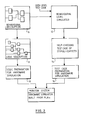
- Figure 2 illustrates the design flow of a simulation strategy using a hardware simulation system composes of programmable logic arrays.
- the left hand side of Figure 2 covers the design of the logic structure.
- First a behavioural description (6) is written to verify the design of the whole system.
- the 'blocks' may be integrated circuits or major portions of integrated circuits.
- This high level design is converted to a detailed logic description (8) either by hand or by logic synthesis.
- This logic description (8) is then prepared by software (10) for use on the hardware simulator. There are two parts to this. The first is to determine how to program each of the PLAs to carry out its allocated part of the logical function. The second is to determine the necessary interconnections. As will be discussed later this interconnection involves the programming of the programmable interconnect logic blocks, which themselves comprise PLAs. All the PLAs will be bulk erased (e.g.
- the output of the software preparation stage can be a file of programming instructions which can be directly applied to the PLAs.
- the hardware simulator contains a model of the integrated circuit being modelled.
- FIG. 2 The right hand side of Figure 2 shows the simulation method.
- the behavioural model When the behavioural model is simulated (12) it produces a self checking test case (14) for the logic level model. This is done by a monitor which records all transitions at the inputs and outputs of a block of logic as if it were the whole system. From these a list of Stimuli and 'Expects' (16) can be generated, one set for each clock cycle. This list is loaded into the monitor system of the hardware simulator. This monitor system applies the first set of stimuli, clocks the programmable logic devices and then checks the appropriate output signals against the expects. No delay simulation is carried out. Timing analysis plus limited software simulation will be adequate for this.
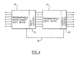
- Figure 3 illustrates the interconnection structure of one embodiment of the invention and Figure 4 illustrates a unit comprising a programmable logic device (PLD) (20) and a programmable interconnect logic block (PILB) (18) from which the structure of Figure 3 is built up.
- the PLDs (20) and the PILBs (18) are programmed PLAs. All the PLDs (20) and PILBs (18) are linked to a data bus (22) extending therebetween. All the PILBs (18) are connected to an address bus (24) extending therebetween.
- the address bus (24) is also connected to an address signal generator (26), whilst the data bus (22) is also connected to a monitor system (28). Both the address signal generator (26) and the monitor system (28) may be embodied within a computer such as a personal computer.
- Each PLD (20) is programmed to perform the same logical function as a portion of the hardware being simulated.
- Associated with each PLD (20) are a set of output latches (32).
- the output latches (32) correspond to latches within the hardware being simulated and store the output signals from their PLD (20) which result from the signal processing carried out by that PLD (20). Some of the output latches will be directly fed back into the PLD (20) to enable the simulation of complex logical functions within the PLD (20).
- Each PILB (18) is programmed to be responsive to the addresses issued by the address generator (26) on the address bus (24).
- the address signal generator (26) and the address bus (24) are specific embodiments of the control signal generator and control bus previously discussed.
- the address signal generator (26) sequentially writes addresses corresponding to selected sets of output latches (32) on to the address bus (24).
- the PILBs watch for the address of their associated set of output latches (32) to be written on the address bus (24) whereupon the PILB (18) triggers (via line (34)) its associated set of output latches (32) to write their stored output signals on to the data bus (22).
- the PILBs (18) are also programmed to look for addresses corresponding to the output latch address from which one of their associated set of input latches (30) must receive stored signals. When such an address is on the address bus (24) the PILB (18) response by connecting the input latch concerned to the appropriate line of the data bus (22) from where the selected input latch reads in and stores the signal value which it will feed to the PLD in the next simulated clock cycle.
- the function of the PILBs (18) is two-fold. They control the writing of signals on to the data bus (22) by associated output latches (32) and they control the read of signals off the data bus (22) by associated input latches (30). Both of these functions are driven by the sequence of addresses written on the address bus (24). When all the sets of output latches have been addressed each output signal will have been written on the data bus (22) from where it should have been picked up by the appropriate input latch (30).
- the monitor system (28) can read and store the values on the data bus (22). These values effectively give a snap shot picture of the state of the simulated hardware and may be compare with the lists of 'Expects' to check that the hardware is behaving as it should. A mismatch between the signals read and stored and the 'Expects' would be indicative of an error in the circuit design. It is possible for the monitor system (28) only to read and store certain key signals within the simulated hardware to compare with its 'Expects'. If a design error was found at this level the monitor system (28) could be reprogrammed to look in more detail at the latches associated with the latch upon which the error was occurring to assist in the solving of the error.
- the monitor system (28) can also be used to supply the 'Stimuli' to the simulator.
- the monitor system will simply wait for the appropriate address to be written on the address bus (24) whereupon it will write the 'Stimuli' signals on to the data bus (22) from where they will be latched up by the appropriate input latches (30).
- the PLDs (20) will all be clocked to simulate a clock cycle of the hardware being simulated.
- the clock signal fed to the PLDs (20) to trigger the simulation of a clock cycle may be provided by the monitor system or may be provided by an external clock source (not shown).
- the appropriate input signals generated in the previous simulated clock signal will have been transferred to their inputs and a new set of output signals will be generated and stored in the output latches (32). These fresh output signals will then be transferred and the process repeated.
- FIG. 5 shows in more detail an implementation of one sixteen bit unit of the invention. Since current PLAs are not optimised for the PILB (18) function, a small Intel 5C90 PLA is used with a separate MSI register serving as the input latches (30).
- the PLD (20) is an Intel 5C180 PLA which provides more inputs and outputs than are needed for a sixteen bit system.
- the auxiliary inputs of one PLD (20) may be connected to the auxiliary outputs of another PLD (20) yielding an increase in the capability of the system.
- Figure 6 illustrates a different embodiment of the invention which enables larger integrated circuits to be simulated without too large an increase in the time taken to transfer all the signals around the simulator between simulated clock cycles.
- Each of the blocks (42) represents a system as illustrated in Figure 3. Each of these systems is linked to a master address bus (38) and a master data bus (40).
- the master address bus corresponds to the master control bus previously described.
- a master control signal generator (44) monitors the operation of each of the monitor systems (28) within the individual blocks and allows the exchange of signals within each block (42) to proceed in parallel. When the signal exchange within the blocks (42) has been completed the master signal generator (44) then proceeds to carry out the necessary signal transfers between the blocks (42) via the master data bus (40) and the master address bus (38).
- the master control signal generator (44) is able to selectively connect the local data and address buses within each of the blocks (42) to the master data and address buses via interposed bus transceivers (36).
- the bus transceivers (36) provide two way switchable gates which allow the local data and address bus in one block (42) to be connected to those of another block via the master data bus (40) and master address bus (38).
- Figures 7 and 8 show alternative expanded system configurations.
- one monitor system is used to control two bus systems.
- the same addresses are supplied to each bus system but the data buses of each can be selectively connected or kept separate by the action of the bus transceivers (36). Accordingly, transfers can take place in parallel within each bus system and the data buses need only be connected when a transfer between bus systems is required.
- the number and size of the local data buses is itself configurable using the bus transceivers (36).
- the same address signal is supplied to each programmable logic device but the grouping of the devices into local block sharing a data bus is controlled by the bus transceivers (36). Accordingly, some local blocks may be small and others large depending upon the circuit being simulated.
- Figures 7 and 8 illustrate the diversity and flexibility of systems using the invention that can be produced.
Abstract
Description
- This invention relates to the field of hardware simulators. More particularly this invention relates to hardware simulators of the type comprising a plurality of interlinked programmable logic devices.
- It is essential when designing and developing integrated circuits to test the design of the circuit before the circuit is manufactured. This testing is done by simulating how a circuit built to that design will operate. The traditional method of logic simulation is to use a software simulator running on a conventional (non parallel) computer. A problem with such methods is that the performance of the simulator is usually millions of times slower than the actual performance of the hardware being simulated. This problem is made worst as the size of the chip becomes larger. With the current generation of Very Large Scale Integration (VLSI) integrated circuits the problem of the time taken to run these simulations is becoming critical.
- One solution to this problem is to use special purpose computers to carry out the simulation. These special purpose computers are parallel processors, typically with up to 256 Central Processor Units (CPUs). Special software prepares the logic being simulated so that the processors may work on it in parallel. These systems are extremely expensive - in some cases millions of dollars.
- An alternative less expensive solution which has been suggested is to use programmable logic devices (PLDs). These are integrated circuits that may be programmed or personalised in a few minutes to perform any logical function or combination of logical functions that may be desired. Known PLDs may be programmed to perform the desired function by the use of fusible links or electrical programming techniques such as those used with Electrically Programmable Read Only Memories (EPROMS). Such programmable logic devices have a much lower density than the VLSI integrated circuits they are simulating and so many tens or possibly hundreds of PLDs may be needed to simulate one VLSI integrated circuit.
- The major problem with this approach is the large number of interconnections that have to be made between the PLDs. The interconnection needs to be specific to the hardware being simulated. In the past the interconnection has been hand-wired which is not only extremely time consuming and error prone but also has the result that when built the simulator is unique to the hardware being simulated and cannot easily be reused. In addition, the control of the wiring and its documentation presents a problem of a similar size to the design and control of the integrated circuit itself. Another problem is ensuring the designs of the simulator and the simulated integrated circuit remain in step as the design of the integrated circuit is modified. All the problems with these hand-wired simulators are made worse as the size of the circuits being simulated increases.
- The invention provides a hardware simulator having a plurality of programmable logic devices, a data bus, a control bus, and a control signal generator, each said device having a set of output latches storing output signals from said device and a set of input latches storing input signals to said device, each said set of input latches and each said set of output latches being selectively connected to said data bus under control of a programmable interconnect logic block, and said control signal generator and each said programmable interconnect logic block being connected to said control bus, such that control signals issued by said control signal generator via said control bus control said programmable interconnect logic blocks to connect selected output latches and selected input latches to said data bus to effect a sequence of signal transfer steps in which stored signals are transferred from said selected output latches to said selected input latches via said data bus.
- The invention provides a hardware simulator in which the interconnections between the PLDs are made by programming the programmable interconnect logic blocks associated with each device. There is no need to hand-wire the connections. This allows a quicker, less error prone and more automated setting up of the simulator. The invention also makes it practical to use this type of PLD simulator to simulate VLSI integrated circuit without the problems of controlling and documenting the interconnection becoming unmanageable. It is also easier to make changes to the interconnections as the design of the integrated circuit being simulated is modified. The key element in the hardware simulator is the programmable interconnect logics blocks which allow random logical interconnections to be made via a regular physical hardware structure. It will be appreciated that the interconnect logic block may be a separate device or may be part of the programmable logic device.
- An example of the operation of this simulator is as follows. The output latches correspond to 'real latches' within the hardware being simulated and the output signals represent the results of the signal processing that has been carried out by the functional logic programmed within the associated PLD during the last simulated clock cycle. The inputs to that functional logic for the last simulated clock cycle were and still are held in the input latches for that PLD. Many of the output latches within the simulator will be holding signals which are in fact required as inputs at other points within the simulator. The task that must be accomplished before the next clock cycle may be simulated is to transfer the signals stored in the output latches to their corresponding input latches as necessary.
- In the prior art this transfer was carried out by the physical link of a piece of wire. No separate input latch being needed as the output latch would also directly store the input signal. The invention provides data and control buses for carrying out the transfer of the signals in the output latches to the input latches where they may then be used to simulate the next clock cycle. The overall operation is that a clock cycle is simulated by the PLDs and then the control signal generator issues a sequence of commands on the control bus to the programmable interconnect logic blocks drive the necessary signal transfers. Each command results in one or more output latches writing their signals on to the data bus and one or more input latches, which may be associated with the same or a different PLD, to read in and store the signals on the data bus. When the complete sequence of commands has been run through all the necessary input signals will be in place and up-to-date and the next clock cycle may be simulated.
- It will be appreciated that the control signals could take a number of forms. What is important is that the programmable interconnect logic devices can interpret the control signals to connect the necessary output latches and input latches to the data bus in the required sequence. One possibility would be to provide a control signal in the form of a master clock signal fed to all the programmable interconnect logic block. The programmable interconnect logic block would have internal clocks synchronised to the master clock and would be programmed to connect the appropriate output latches and input latches to the data bus at predetermined times relative to the master clock signal.
- In preferred embodiments of the invention said control signals comprise multibit address signals, and each said address signal identifies selected output latches and selected input latches to be connected to said data bus by said programmable interconnect logic blocks. This arrangement permits each data transfer to be individually addressed and allows considerable flexibility in the number, sequencing and timing of the data transfers.
- Another preferred feature of the invention concerns the manner in which external input signals may be fed to the simulator to test its response in differing conditions and the manner in which diagnostic information is read from the simulator. Preferred embodiments of the invention include a monitor system linked to said data bus and said control bus, said monitor system being responsive to said control signals to read and store output signals from said data bus and to write stimulus signals on to said data bus to be stored in selected input latches. This preferred embodiment allows the monitor system to take advantage of the existing system provided by the hardware simulator to transfer signals between input latches and output latches to feed stimuli into the simulator and read the state of the latches out of the simulator.
- It will be appreciated that the majority of the time taken to run a simulation with the present invention is taken up with transfer of the signals between the output latches and the input latches. As the size of the integrated circuit increases so the total number of latches to be simulated increases. Simplistically, one would expect an approximately linear increase in simulation time with the number of latches to be simulated. However, most VLSI circuits are composed of a number of quasi self-contained units or functional islands which have relatively few latches in communications with other parts of the integrated circuit. Preferred embodiments of the invention exploit this fact by providing a hardware simulator according to the invention linked to one or more further hardware simulators according to the invention by a master data bus and a master control bus, wherein a master control signal generator issues master control signals on said master control bus control to said hardware simulators to transfer signals from selected output latches in a first hardware simulator to selected input latches in a second hardware simulator via said master data bus.
- Thus it will be seen that the hardware simulators may carry out their internal signal transfers in parallel with the smaller number of signal transfers between hardware simulators (each corresponding to a functional island) taking place separately. This feature allows VLSI integrated circuits to be simulated without the simulation times becoming too large.
- In preferred embodiments of the invention said programmable logic devices comprise electrically programmable logic arrays (EPLAs). Such EPLAs may easily be programmed using automated techniques thereby reducing the time taken to configure the hardware simulator and the likelihood of error. Similarly, in preferred embodiments of the invention said programmable interconnect logic blocks comprise electrically programmable logic arrays.
- Preferred embodiments of the invention will now be described, by way of example only, with reference to the accompanying drawings in which:
- Figure 1 illustrates the prior art interconnection system for the programmable logic arrays.
- Figure 2 illustrates the simulation strategy when using a hardware simulator composed of programmable logic arrays.
- Figure 3 illustrates the interconnection structure of one embodiment of the invention.
- Figure 4 illustrates a programmable logic device / programmable interconnect logic block unit of one embodiment of the invention.
- Figure 5 illustrates in more detail the programmable logic device / programmable interconnect logic block shown in Figure 4.
- Figures 6, 7 and 8 illustrate alternative embodiments for interconnection systems for use when simulation integrated circuits have a large number of latches.
- Figure 1 illustrates a known interconnection system for a hardware simulator comprising a plurality of programmable logic arrays (PLAs) (2). As can be seen the hand-wired links (4) are complex even for the relatively small numbers of PLAs (2) shown. As the number of PLAs (2) increases the complexity and unsuitability of hand-wired links (4) rapidly increases. There is no pattern to the interconnection, it is unique to the integrated circuit being simulated.
- Figure 2 illustrates the design flow of a simulation strategy using a hardware simulation system composes of programmable logic arrays.
- The left hand side of Figure 2 covers the design of the logic structure. First a behavioural description (6) is written to verify the design of the whole system. The 'blocks' may be integrated circuits or major portions of integrated circuits. This high level design is converted to a detailed logic description (8) either by hand or by logic synthesis. This logic description (8) is then prepared by software (10) for use on the hardware simulator. There are two parts to this. The first is to determine how to program each of the PLAs to carry out its allocated part of the logical function. The second is to determine the necessary interconnections. As will be discussed later this interconnection involves the programming of the programmable interconnect logic blocks, which themselves comprise PLAs. All the PLAs will be bulk erased (e.g. by exposure to UV light) on their cards and then programmed in situ. The output of the software preparation stage can be a file of programming instructions which can be directly applied to the PLAs. Once the PLAs have been programmed the hardware simulator contains a model of the integrated circuit being modelled.
- The right hand side of Figure 2 shows the simulation method. When the behavioural model is simulated (12) it produces a self checking test case (14) for the logic level model. This is done by a monitor which records all transitions at the inputs and outputs of a block of logic as if it were the whole system. From these a list of Stimuli and 'Expects' (16) can be generated, one set for each clock cycle. This list is loaded into the monitor system of the hardware simulator. This monitor system applies the first set of stimuli, clocks the programmable logic devices and then checks the appropriate output signals against the expects. No delay simulation is carried out. Timing analysis plus limited software simulation will be adequate for this.
- Figure 3 illustrates the interconnection structure of one embodiment of the invention and Figure 4 illustrates a unit comprising a programmable logic device (PLD) (20) and a programmable interconnect logic block (PILB) (18) from which the structure of Figure 3 is built up. The PLDs (20) and the PILBs (18) are programmed PLAs. All the PLDs (20) and PILBs (18) are linked to a data bus (22) extending therebetween. All the PILBs (18) are connected to an address bus (24) extending therebetween. The address bus (24) is also connected to an address signal generator (26), whilst the data bus (22) is also connected to a monitor system (28). Both the address signal generator (26) and the monitor system (28) may be embodied within a computer such as a personal computer.
- Each PLD (20) is programmed to perform the same logical function as a portion of the hardware being simulated. Associated with each PLD (20) are a set of output latches (32). The output latches (32) correspond to latches within the hardware being simulated and store the output signals from their PLD (20) which result from the signal processing carried out by that PLD (20). Some of the output latches will be directly fed back into the PLD (20) to enable the simulation of complex logical functions within the PLD (20).
- Each PILB (18) is programmed to be responsive to the addresses issued by the address generator (26) on the address bus (24). The address signal generator (26) and the address bus (24) are specific embodiments of the control signal generator and control bus previously discussed. The address signal generator (26) sequentially writes addresses corresponding to selected sets of output latches (32) on to the address bus (24). The PILBs watch for the address of their associated set of output latches (32) to be written on the address bus (24) whereupon the PILB (18) triggers (via line (34)) its associated set of output latches (32) to write their stored output signals on to the data bus (22). The PILBs (18) are also programmed to look for addresses corresponding to the output latch address from which one of their associated set of input latches (30) must receive stored signals. When such an address is on the address bus (24) the PILB (18) response by connecting the input latch concerned to the appropriate line of the data bus (22) from where the selected input latch reads in and stores the signal value which it will feed to the PLD in the next simulated clock cycle.
- Thus it can be seen that the function of the PILBs (18) is two-fold. They control the writing of signals on to the data bus (22) by associated output latches (32) and they control the read of signals off the data bus (22) by associated input latches (30). Both of these functions are driven by the sequence of addresses written on the address bus (24). When all the sets of output latches have been addressed each output signal will have been written on the data bus (22) from where it should have been picked up by the appropriate input latch (30).
- Whilst this signal transfer is taking place between the various output and input latches the monitor system (28) can read and store the values on the data bus (22). These values effectively give a snap shot picture of the state of the simulated hardware and may be compare with the lists of 'Expects' to check that the hardware is behaving as it should. A mismatch between the signals read and stored and the 'Expects' would be indicative of an error in the circuit design. It is possible for the monitor system (28) only to read and store certain key signals within the simulated hardware to compare with its 'Expects'. If a design error was found at this level the monitor system (28) could be reprogrammed to look in more detail at the latches associated with the latch upon which the error was occurring to assist in the solving of the error.
- The monitor system (28) can also be used to supply the 'Stimuli' to the simulator. The monitor system will simply wait for the appropriate address to be written on the address bus (24) whereupon it will write the 'Stimuli' signals on to the data bus (22) from where they will be latched up by the appropriate input latches (30).
- Once all the signal transfers have been completed the PLDs (20) will all be clocked to simulate a clock cycle of the hardware being simulated. The clock signal fed to the PLDs (20) to trigger the simulation of a clock cycle may be provided by the monitor system or may be provided by an external clock source (not shown). The appropriate input signals generated in the previous simulated clock signal will have been transferred to their inputs and a new set of output signals will be generated and stored in the output latches (32). These fresh output signals will then be transferred and the process repeated.
- Figure 5 shows in more detail an implementation of one sixteen bit unit of the invention. Since current PLAs are not optimised for the PILB (18) function, a small Intel 5C90 PLA is used with a separate MSI register serving as the input latches (30). The PLD (20) is an Intel 5C180 PLA which provides more inputs and outputs than are needed for a sixteen bit system. The auxiliary inputs of one PLD (20) may be connected to the auxiliary outputs of another PLD (20) yielding an increase in the capability of the system.
- As previously mentioned it is possible to increase the size of the simulator by simply adding more units to the data bus (22) and the address bus (24). However, simply adding units to the bus in this way would increase the time taken to address every latch and complete a data transfer cycle before the next clock cycle could be simulated. Figure 6 illustrates a different embodiment of the invention which enables larger integrated circuits to be simulated without too large an increase in the time taken to transfer all the signals around the simulator between simulated clock cycles.
- Each of the blocks (42) represents a system as illustrated in Figure 3. Each of these systems is linked to a master address bus (38) and a master data bus (40). The master address bus corresponds to the master control bus previously described. A master control signal generator (44) monitors the operation of each of the monitor systems (28) within the individual blocks and allows the exchange of signals within each block (42) to proceed in parallel. When the signal exchange within the blocks (42) has been completed the master signal generator (44) then proceeds to carry out the necessary signal transfers between the blocks (42) via the master data bus (40) and the master address bus (38). The master control signal generator (44) is able to selectively connect the local data and address buses within each of the blocks (42) to the master data and address buses via interposed bus transceivers (36). The bus transceivers (36) provide two way switchable gates which allow the local data and address bus in one block (42) to be connected to those of another block via the master data bus (40) and master address bus (38).
- The overall operation of this system is that first all the local signal transfers are completed in parallel and then the necessary transfers are undertaken between the blocks (42).
- Figures 7 and 8 show alternative expanded system configurations. In the embodiment of Figure 7 one monitor system is used to control two bus systems. The same addresses are supplied to each bus system but the data buses of each can be selectively connected or kept separate by the action of the bus transceivers (36). Accordingly, transfers can take place in parallel within each bus system and the data buses need only be connected when a transfer between bus systems is required. In the embodiment of Figure 8 the number and size of the local data buses is itself configurable using the bus transceivers (36). The same address signal is supplied to each programmable logic device but the grouping of the devices into local block sharing a data bus is controlled by the bus transceivers (36). Accordingly, some local blocks may be small and others large depending upon the circuit being simulated. Figures 7 and 8 illustrate the diversity and flexibility of systems using the invention that can be produced.
Claims (6)
- A hardware simulator having a plurality of programmable logic devices (20), a data bus (22), a control bus (24), and a control signal generator (26), each said device having a set of output latches (32) storing output signals from said device and a set of input latches (30) storing input signals to said device, each said set of input latches and each said set of output latches being selectively connected to said data bus under control of a programmable interconnect logic block (18), and said control signal generator and each said programmable interconnect logic block being connected to said control bus, such that control signals issued by said control signal generator via said control bus control said programmable interconnect logic blocks to connect selected output latches and selected input latches to said data bus to effect a sequence of signal transfer steps in which stored signals are transferred from said selected output latches to said selected input latches via said data bus.
- A hardware simulator as claimed in claim 1, wherein said control signals comprise multibit address signals, and each said address signal identifies selected output latches and selected input latches to be connected to said data bus by said programmable interconnect logic blocks.
- A hardware simulator as claimed in claims 1 or 2, further comprising a monitor system (28) linked to said data bus and said control bus, said monitor system being responsive to said control signals to read and store output signals from said data bus and to write stimulus signals on to said data bus to be stored in selected input latches.
- A hardware simulator as claimed in claims 1, 2 or 3, wherein said programmable logic devices comprise electrically programmable logic arrays.
- A hardware simulator as claimed in any preceding claim, wherein said programmable interconnect logic blocks comprise electrically programmable logic arrays.
- A hardware simulator (42) as claimed in any preceding claimed linked to one or more further hardware simulators (42) as claimed in any preceding claim by a master data bus (40) and a master control bus (38), wherein a master control signal generator (44) issues master control signals on said master control bus control to said hardware simulators to transfer signals from selected output latches in a first hardware simulator to selected input latches in a second hardware simulator via said master data bus.
Priority Applications (4)
| Application Number | Priority Date | Filing Date | Title |
|---|---|---|---|
| DE69030953T DE69030953D1 (en) | 1990-03-08 | 1990-03-08 | Hardware simulator |
| EP90302520A EP0445454B1 (en) | 1990-03-08 | 1990-03-08 | Hardware simulator |
| US07/657,705 US5263149A (en) | 1990-03-08 | 1991-02-19 | Integrated circuit logic functions simulator for selectively connected series of preprogrammed PLA devices using generated sequence of address signals being provided between simulated clock cycles |
| JP3050308A JPH0713654B2 (en) | 1990-03-08 | 1991-02-25 | Hardware simulator |
Applications Claiming Priority (1)
| Application Number | Priority Date | Filing Date | Title |
|---|---|---|---|
| EP90302520A EP0445454B1 (en) | 1990-03-08 | 1990-03-08 | Hardware simulator |
Publications (2)
| Publication Number | Publication Date |
|---|---|
| EP0445454A1 true EP0445454A1 (en) | 1991-09-11 |
| EP0445454B1 EP0445454B1 (en) | 1997-06-18 |
Family
ID=8205320
Family Applications (1)
| Application Number | Title | Priority Date | Filing Date |
|---|---|---|---|
| EP90302520A Expired - Lifetime EP0445454B1 (en) | 1990-03-08 | 1990-03-08 | Hardware simulator |
Country Status (4)
| Country | Link |
|---|---|
| US (1) | US5263149A (en) |
| EP (1) | EP0445454B1 (en) |
| JP (1) | JPH0713654B2 (en) |
| DE (1) | DE69030953D1 (en) |
Cited By (2)
| Publication number | Priority date | Publication date | Assignee | Title |
|---|---|---|---|---|
| ES2167209A1 (en) * | 2000-02-14 | 2002-05-01 | Univ Vigo | Digital circuit emulator. |
| EP1475727A1 (en) * | 2003-05-07 | 2004-11-10 | Arteris | Device for emulating one or more IC chips |
Families Citing this family (34)
| Publication number | Priority date | Publication date | Assignee | Title |
|---|---|---|---|---|
| US5452231A (en) * | 1988-10-05 | 1995-09-19 | Quickturn Design Systems, Inc. | Hierarchically connected reconfigurable logic assembly |
| US5452227A (en) * | 1991-11-13 | 1995-09-19 | Westinghouse Elec. Corp. | Method and apparatus for converting a programmable logic device designed into a selectable target gate array design |
| JP2941135B2 (en) * | 1992-01-24 | 1999-08-25 | 富士通株式会社 | Pseudo LSI device and debug device using the same |
| JP3500633B2 (en) * | 1992-02-07 | 2004-02-23 | セイコーエプソン株式会社 | Microelectronic device emulation method, emulation apparatus and simulation apparatus |
| DE4211162C2 (en) * | 1992-03-31 | 1996-03-21 | Manfred Dipl Ing Zeiner | Hardware emulation system |
| US5404496A (en) * | 1992-07-01 | 1995-04-04 | Hewlett-Packard Company | Computer-based system and method for debugging a computer system implementation |
| US5913051A (en) * | 1992-10-09 | 1999-06-15 | Texas Instruments Incorporated | Method of simultaneous simulation of a complex system comprised of objects having structure state and parameter information |
| US5452229A (en) * | 1992-12-18 | 1995-09-19 | Lattice Semiconductor Corporation | Programmable integrated-circuit switch |
| FR2712998B1 (en) * | 1993-11-22 | 1996-02-09 | Aerospatiale | Digital bus simulator integrated into an automatic test system for electronic boxes on board aircraft. |
| US5721695A (en) * | 1994-10-17 | 1998-02-24 | Advanced Micro Devices, Inc. | Simulation by emulating level sensitive latches with edge trigger latches |
| US5724504A (en) * | 1995-06-01 | 1998-03-03 | International Business Machines Corporation | Method for measuring architectural test coverage for design verification and building conformal test |
| US6526461B1 (en) * | 1996-07-18 | 2003-02-25 | Altera Corporation | Interconnect chip for programmable logic devices |
| US5892940A (en) * | 1996-12-05 | 1999-04-06 | Hewlett-Packard, Co. | Aliasing nodes to improve the code generated by a circuit compiler |
| US5819074A (en) * | 1996-12-05 | 1998-10-06 | Hewlett-Packard Co. | Method of eliminating unnecessary code generation in a circuit compiler |
| AUPO493597A0 (en) * | 1997-02-05 | 1997-02-27 | Liguori, Vincenzo | Logic circuit emulator |
| US6009256A (en) * | 1997-05-02 | 1999-12-28 | Axis Systems, Inc. | Simulation/emulation system and method |
| US6321366B1 (en) | 1997-05-02 | 2001-11-20 | Axis Systems, Inc. | Timing-insensitive glitch-free logic system and method |
| US6134516A (en) * | 1997-05-02 | 2000-10-17 | Axis Systems, Inc. | Simulation server system and method |
| US6389379B1 (en) | 1997-05-02 | 2002-05-14 | Axis Systems, Inc. | Converification system and method |
| US6421251B1 (en) | 1997-05-02 | 2002-07-16 | Axis Systems Inc | Array board interconnect system and method |
| US6026230A (en) * | 1997-05-02 | 2000-02-15 | Axis Systems, Inc. | Memory simulation system and method |
| US6016554A (en) * | 1997-07-28 | 2000-01-18 | Advanced Micro Devices, Inc. | Method for event-related functional testing of a microprocessor |
| US5963722A (en) * | 1997-07-31 | 1999-10-05 | Advanced Micro Devices, Inc. | Byte granularity data checking in a bus bridge verification system |
| US5961625A (en) * | 1997-07-31 | 1999-10-05 | Advanced Micro Devices, Inc. | Bus bridge state monitoring in a bus bridge verification system |
| US6112312A (en) * | 1998-03-10 | 2000-08-29 | Advanced Micro Devices, Inc. | Method for generating functional tests for a microprocessor having several operating modes and features |
| US6167364A (en) * | 1998-04-17 | 2000-12-26 | Altera Corporation | Methods and apparatus for automatically generating interconnect patterns in programmable logic devices |
| US6618698B1 (en) | 1999-08-12 | 2003-09-09 | Quickturn Design Systems, Inc. | Clustered processors in an emulation engine |
| US6985840B1 (en) * | 2000-07-31 | 2006-01-10 | Novas Software, Inc. | Circuit property verification system |
| US7343279B2 (en) * | 2002-08-01 | 2008-03-11 | Teradyne, Inc. | Universal approach for simulating, emulating, and testing a variety of serial bus types |
| US7428218B2 (en) * | 2002-08-01 | 2008-09-23 | Teradyne, Inc. | Flexible approach for representing different bus protocols |
| KR101006665B1 (en) * | 2003-12-22 | 2011-01-10 | 엘지전자 주식회사 | Subscriber identity module simulator using programmable logic device |
| US7315972B1 (en) * | 2004-05-20 | 2008-01-01 | Xilinx, Inc. | Method and apparatus for automated generation of expected value data for circuit designs |
| US8346527B2 (en) * | 2008-01-14 | 2013-01-01 | International Business Machines Corporation | Simulating an operation of a digital circuit |
| US8706467B2 (en) * | 2008-04-02 | 2014-04-22 | Synopsys, Inc. | Compact circuit-simulation output |
Citations (2)
| Publication number | Priority date | Publication date | Assignee | Title |
|---|---|---|---|---|
| EP0076494A2 (en) * | 1981-10-07 | 1983-04-13 | Hitachi, Ltd. | Data transmission bus system for a plurality of processors |
| FR2578338A1 (en) * | 1985-03-01 | 1986-09-05 | Simulog Inc | LOGIC SIMULATOR CABLE |
Family Cites Families (6)
| Publication number | Priority date | Publication date | Assignee | Title |
|---|---|---|---|---|
| US4306286A (en) * | 1979-06-29 | 1981-12-15 | International Business Machines Corporation | Logic simulation machine |
| US4821173A (en) * | 1986-06-30 | 1989-04-11 | Motorola, Inc. | Wired "OR" bus evaluator for logic simulation |
| US4852083A (en) * | 1987-06-22 | 1989-07-25 | Texas Instruments Incorporated | Digital crossbar switch |
| US4916647A (en) * | 1987-06-26 | 1990-04-10 | Daisy Systems Corporation | Hardwired pipeline processor for logic simulation |
| EP0437491B1 (en) * | 1988-10-05 | 1995-12-13 | Quickturn Systems Inc | Method of using electronically reconfigurable gate array logic and apparatus formed thereby |
| US5109353A (en) * | 1988-12-02 | 1992-04-28 | Quickturn Systems, Incorporated | Apparatus for emulation of electronic hardware system |
-
1990
- 1990-03-08 EP EP90302520A patent/EP0445454B1/en not_active Expired - Lifetime
- 1990-03-08 DE DE69030953T patent/DE69030953D1/en not_active Expired - Lifetime
-
1991
- 1991-02-19 US US07/657,705 patent/US5263149A/en not_active Expired - Fee Related
- 1991-02-25 JP JP3050308A patent/JPH0713654B2/en not_active Expired - Lifetime
Patent Citations (2)
| Publication number | Priority date | Publication date | Assignee | Title |
|---|---|---|---|---|
| EP0076494A2 (en) * | 1981-10-07 | 1983-04-13 | Hitachi, Ltd. | Data transmission bus system for a plurality of processors |
| FR2578338A1 (en) * | 1985-03-01 | 1986-09-05 | Simulog Inc | LOGIC SIMULATOR CABLE |
Cited By (3)
| Publication number | Priority date | Publication date | Assignee | Title |
|---|---|---|---|---|
| ES2167209A1 (en) * | 2000-02-14 | 2002-05-01 | Univ Vigo | Digital circuit emulator. |
| EP1475727A1 (en) * | 2003-05-07 | 2004-11-10 | Arteris | Device for emulating one or more IC chips |
| FR2854703A1 (en) * | 2003-05-07 | 2004-11-12 | Arteris | DEVICE FOR EMULATING ONE OR MORE CHIPS OF INTEGRATED CIRCUITS |
Also Published As
| Publication number | Publication date |
|---|---|
| EP0445454B1 (en) | 1997-06-18 |
| JPH0713654B2 (en) | 1995-02-15 |
| JPH05249184A (en) | 1993-09-28 |
| US5263149A (en) | 1993-11-16 |
| DE69030953D1 (en) | 1997-07-24 |
Similar Documents
| Publication | Publication Date | Title |
|---|---|---|
| EP0445454B1 (en) | Hardware simulator | |
| US7185293B1 (en) | Universal hardware device and method and tools for use therewith | |
| Trimberger | A reprogrammable gate array and applications | |
| US5940603A (en) | Method and apparatus for emulating multi-ported memory circuits | |
| US6701491B1 (en) | Input/output probing apparatus and input/output probing method using the same, and mixed emulation/simulation method based on it | |
| US8108729B2 (en) | Memory-based trigger generation scheme in an emulation environment | |
| EP0651343B1 (en) | Method of using electronically reconfigurable gate array logic and apparatus formed thereby | |
| US6035117A (en) | Tightly coupled emulation processors | |
| JP4664056B2 (en) | Device that emulates the operation of electronic equipment | |
| EP0336243A2 (en) | Massively distributed simulation engine | |
| JPH08507628A (en) | A mask program integrated circuit having timing and logic compatibility with a user-arranged logic array. | |
| US8270231B2 (en) | Configurable embedded processor | |
| JPS5832780B2 (en) | Testable large-scale integrated circuit chips | |
| KR19990077413A (en) | Emulation module having planar array organization | |
| WO1993016433A1 (en) | Hardware emulation accelerator and method | |
| US5386550A (en) | Pseudo-LSI device and debugging system incorporating same | |
| Stroud | Automated BIST for sequential logic synthesis | |
| Cruz et al. | SUE: A special purpose computer for spin glass models | |
| US7480611B2 (en) | Method and apparatus to increase the usable memory capacity of a logic simulation hardware emulator/accelerator | |
| KR100710972B1 (en) | Mixed Verification Apparatus for Mixed Emulation/Simulation and Mixed Verification Method Using the Same | |
| JP3999290B2 (en) | Semiconductor test equipment | |
| EP1236222B1 (en) | Universal hardware device and method and tools for use therewith | |
| Denneau et al. | Design and implementation of a software simulation engine | |
| Lo et al. | Hardware emulation board based on FPGAs and programmable interconnections | |
| JPS62150181A (en) | Test system for large-scale integrated circuit |
Legal Events
| Date | Code | Title | Description |
|---|---|---|---|
| PUAI | Public reference made under article 153(3) epc to a published international application that has entered the european phase |
Free format text: ORIGINAL CODE: 0009012 |
|
| AK | Designated contracting states |
Kind code of ref document: A1 Designated state(s): DE FR GB |
|
| 17P | Request for examination filed |
Effective date: 19911219 |
|
| 17Q | First examination report despatched |
Effective date: 19940928 |
|
| GRAG | Despatch of communication of intention to grant |
Free format text: ORIGINAL CODE: EPIDOS AGRA |
|
| GRAH | Despatch of communication of intention to grant a patent |
Free format text: ORIGINAL CODE: EPIDOS IGRA |
|
| GRAH | Despatch of communication of intention to grant a patent |
Free format text: ORIGINAL CODE: EPIDOS IGRA |
|
| GRAA | (expected) grant |
Free format text: ORIGINAL CODE: 0009210 |
|
| AK | Designated contracting states |
Kind code of ref document: B1 Designated state(s): DE FR GB |
|
| PG25 | Lapsed in a contracting state [announced via postgrant information from national office to epo] |
Ref country code: FR Effective date: 19970618 |
|
| REF | Corresponds to: |
Ref document number: 69030953 Country of ref document: DE Date of ref document: 19970724 |
|
| PG25 | Lapsed in a contracting state [announced via postgrant information from national office to epo] |
Ref country code: DE Effective date: 19970919 |
|
| EN | Fr: translation not filed | ||
| PGFP | Annual fee paid to national office [announced via postgrant information from national office to epo] |
Ref country code: GB Payment date: 19980218 Year of fee payment: 9 |
|
| PLBE | No opposition filed within time limit |
Free format text: ORIGINAL CODE: 0009261 |
|
| STAA | Information on the status of an ep patent application or granted ep patent |
Free format text: STATUS: NO OPPOSITION FILED WITHIN TIME LIMIT |
|
| 26N | No opposition filed | ||
| PG25 | Lapsed in a contracting state [announced via postgrant information from national office to epo] |
Ref country code: GB Free format text: LAPSE BECAUSE OF NON-PAYMENT OF DUE FEES Effective date: 19990308 |
|
| GBPC | Gb: european patent ceased through non-payment of renewal fee |
Effective date: 19990308 |