EP0435534B1 - Method of manufacturing integrated circuit and integrated circuit made thereby - Google Patents
Method of manufacturing integrated circuit and integrated circuit made thereby Download PDFInfo
- Publication number
- EP0435534B1 EP0435534B1 EP90313667A EP90313667A EP0435534B1 EP 0435534 B1 EP0435534 B1 EP 0435534B1 EP 90313667 A EP90313667 A EP 90313667A EP 90313667 A EP90313667 A EP 90313667A EP 0435534 B1 EP0435534 B1 EP 0435534B1
- Authority
- EP
- European Patent Office
- Prior art keywords
- polycrystalline silicon
- layer
- silicon layer
- insulating layer
- predetermined area
- Prior art date
- Legal status (The legal status is an assumption and is not a legal conclusion. Google has not performed a legal analysis and makes no representation as to the accuracy of the status listed.)
- Expired - Lifetime
Links
Images


Classifications
-
- H—ELECTRICITY
- H10—SEMICONDUCTOR DEVICES; ELECTRIC SOLID-STATE DEVICES NOT OTHERWISE PROVIDED FOR
- H10D—INORGANIC ELECTRIC SEMICONDUCTOR DEVICES
- H10D84/00—Integrated devices formed in or on semiconductor substrates that comprise only semiconducting layers, e.g. on Si wafers or on GaAs-on-Si wafers
- H10D84/01—Manufacture or treatment
- H10D84/0123—Integrating together multiple components covered by H10D12/00 or H10D30/00, e.g. integrating multiple IGBTs
- H10D84/0126—Integrating together multiple components covered by H10D12/00 or H10D30/00, e.g. integrating multiple IGBTs the components including insulated gates, e.g. IGFETs
- H10D84/0165—Integrating together multiple components covered by H10D12/00 or H10D30/00, e.g. integrating multiple IGBTs the components including insulated gates, e.g. IGFETs the components including complementary IGFETs, e.g. CMOS devices
- H10D84/0172—Manufacturing their gate conductors
- H10D84/0177—Manufacturing their gate conductors the gate conductors having different materials or different implants
-
- H—ELECTRICITY
- H10—SEMICONDUCTOR DEVICES; ELECTRIC SOLID-STATE DEVICES NOT OTHERWISE PROVIDED FOR
- H10B—ELECTRONIC MEMORY DEVICES
- H10B41/00—Electrically erasable-and-programmable ROM [EEPROM] devices comprising floating gates
- H10B41/40—Electrically erasable-and-programmable ROM [EEPROM] devices comprising floating gates characterised by the peripheral circuit region
-
- H—ELECTRICITY
- H10—SEMICONDUCTOR DEVICES; ELECTRIC SOLID-STATE DEVICES NOT OTHERWISE PROVIDED FOR
- H10B—ELECTRONIC MEMORY DEVICES
- H10B41/00—Electrically erasable-and-programmable ROM [EEPROM] devices comprising floating gates
- H10B41/40—Electrically erasable-and-programmable ROM [EEPROM] devices comprising floating gates characterised by the peripheral circuit region
- H10B41/42—Simultaneous manufacture of periphery and memory cells
- H10B41/43—Simultaneous manufacture of periphery and memory cells comprising only one type of peripheral transistor
- H10B41/48—Simultaneous manufacture of periphery and memory cells comprising only one type of peripheral transistor with a tunnel dielectric layer also being used as part of the peripheral transistor
-
- H—ELECTRICITY
- H10—SEMICONDUCTOR DEVICES; ELECTRIC SOLID-STATE DEVICES NOT OTHERWISE PROVIDED FOR
- H10D—INORGANIC ELECTRIC SEMICONDUCTOR DEVICES
- H10D1/00—Resistors, capacitors or inductors
- H10D1/60—Capacitors
- H10D1/68—Capacitors having no potential barriers
-
- H—ELECTRICITY
- H10—SEMICONDUCTOR DEVICES; ELECTRIC SOLID-STATE DEVICES NOT OTHERWISE PROVIDED FOR
- H10D—INORGANIC ELECTRIC SEMICONDUCTOR DEVICES
- H10D84/00—Integrated devices formed in or on semiconductor substrates that comprise only semiconducting layers, e.g. on Si wafers or on GaAs-on-Si wafers
- H10D84/01—Manufacture or treatment
- H10D84/02—Manufacture or treatment characterised by using material-based technologies
- H10D84/03—Manufacture or treatment characterised by using material-based technologies using Group IV technology, e.g. silicon technology or silicon-carbide [SiC] technology
- H10D84/038—Manufacture or treatment characterised by using material-based technologies using Group IV technology, e.g. silicon technology or silicon-carbide [SiC] technology using silicon technology, e.g. SiGe
-
- H—ELECTRICITY
- H10—SEMICONDUCTOR DEVICES; ELECTRIC SOLID-STATE DEVICES NOT OTHERWISE PROVIDED FOR
- H10D—INORGANIC ELECTRIC SEMICONDUCTOR DEVICES
- H10D88/00—Three-dimensional [3D] integrated devices
-
- H—ELECTRICITY
- H10—SEMICONDUCTOR DEVICES; ELECTRIC SOLID-STATE DEVICES NOT OTHERWISE PROVIDED FOR
- H10D—INORGANIC ELECTRIC SEMICONDUCTOR DEVICES
- H10D88/00—Three-dimensional [3D] integrated devices
- H10D88/01—Manufacture or treatment
-
- Y—GENERAL TAGGING OF NEW TECHNOLOGICAL DEVELOPMENTS; GENERAL TAGGING OF CROSS-SECTIONAL TECHNOLOGIES SPANNING OVER SEVERAL SECTIONS OF THE IPC; TECHNICAL SUBJECTS COVERED BY FORMER USPC CROSS-REFERENCE ART COLLECTIONS [XRACs] AND DIGESTS
- Y10—TECHNICAL SUBJECTS COVERED BY FORMER USPC
- Y10S—TECHNICAL SUBJECTS COVERED BY FORMER USPC CROSS-REFERENCE ART COLLECTIONS [XRACs] AND DIGESTS
- Y10S148/00—Metal treatment
- Y10S148/014—Capacitor
Definitions
- the present invention relates to a method of manufacturing integrated circuits and to integrated circuits made thereby.
- Integrated circuits such as microprocessors or microcontrollers are known which form complex circuit systems generally comprising a memory unit, a processing unit and input and output interface circuits.
- the memory units comprise matrices of random access memory (RAM) cells, matrices of non-volatile fixed program memory (ROM) cells and matrices of non-volatile electrically programmable memory (EPROM and/or EEPROM) cells having two levels of polycrystalline silicon.
- RAM random access memory
- ROM non-volatile fixed program memory
- EPROM and/or EEPROM electrically programmable memory
- the EPROM and EEPROM memory cells and the capacitors have a structure which is similar in certain respects, since they both have two electrodes separated by a dielectric, as a result of which some of the stages of manufacture of these two types of components may in principle be common.
- the functional characteristics of the memory cells and capacitors are, as is known, very different and, if the same manufacturing stages are to be used for both, it is necessary to make use of compromise solutions which do not make it possible to obtain structures which are most advantageous for correct operation and maximum integration density for either the memory cells or the capacitors.
- a conventional technique for the manufacture of integrated circuits of this type comprises the deposition of a first layer of polycrystalline silicon to form the "floating" gate electrodes of the memory cells and first electrodes of the capacitors, the formation of a layer of silicon dioxide by growth at a high temperature so as to form the so-called “interpoly" dielectric of the memory cells and the dielectric of the capacitors and then the deposition of a second layer of polycrystalline silicon to form the control electrodes of the cells and the second electrodes of the capacitors.
- One way of partially remedying the drawbacks of the prior art would be to increase the doping of the polycrystalline silicon solely in the capacitor zones, by suitable masking and implantation operations thereon.
- the capacitors would have fairly low voltage coefficients, but would nevertheless be subject to the constraints imposed by the thickness and physical characteristics of the dielectric desired for the memory cells.
- the dimensioning of the capacitors would be rather critical since it would be conditioned by a method parameter which is difficult to control, i.e. the doping of the first polycrystalline silicon layer.
- the rate of growth of the oxide depends on the doping of the underlying silicon.
- a third level of polycrystalline silicon is used for the integration of capacitors and memory cells having two levels of polycrystalline silicon without the drawbacks of the prior art.
- EP-A-0 294 699 discloses a method of making capacitors in CMOS and NMOS processes.
- Figs. 1 to 3 are partial sectional views of a silicon wafer during three separate stages of a method constituting an embodiment of the invention.
- the method initially comprises operations of conventional type for the manufacture of integrated circuits with complementary MOS transistors (CMOS).
- CMOS complementary MOS transistors
- a substrate 1 of semiconductor material of a first type of conductivity for instance p-doped monocrystalline silicon
- pockets 2 of opposite conductivity i.e. n-doped, by appropriate masking, doping and diffusion operations. These pockets are designed to contain p-channel transistors.
- a layer of inert material typically silicon nitride, is then deposited and is masked and shaped to form the active areas, i.e. those areas designed to contain transistors and memory cells.
- n-type and p-type doping ions are then implanted to increase the concentration of predetermined zones at the edges of the active areas for the formation of isolating or "channel stopper" regions.
- a high temperature (900-1000°C) operation is then carried out in an oxidizing atmosphere in order to grow the so-called field oxide, i.e. comparatively thick portions of silicon dioxide, shown at 4 in the drawings, only in the zones not covered by the silicon nitride. All the doping species contained in the structure are caused to diffuse so as to obtain p-type isolating regions 3′, shown by p+, in the substrate p and n-type regions 3 ⁇ , shown by n+, in the pockets n (only one of which is shown in the drawings).
- nitride layer After the removal of the nitride layer, appropriate masking and implantation operations are carried out to increase the concentration of p-type doping agents in the active zones designed to contain EPROM memory cells, shown at 5 in the drawings. Oxidation is then carried out to grow a thin layer (for instance 150-500 A) of silicon dioxide on the active zones for the subsequent formation of the gate dielectric of the transistors and memory cells. A polycrystalline silicon layer 7 is then deposited and doped and masking and etching operations are carried out to open up parallel slots in this layer in order to isolate the zones in which the memory cells are to be formed.
- a thin layer for instance 150-500 A
- a polycrystalline silicon layer 7 is then deposited and doped and masking and etching operations are carried out to open up parallel slots in this layer in order to isolate the zones in which the memory cells are to be formed.
- an insulating layer 8 for instance of silicon dioxide, is formed by oxidation at high temperature and a thin layer (for instance 500 A) of polycrystalline silicon 9 is deposited thereon.
- Successive masking and chemical etching operations are then carried out to remove the polycrystalline silicon layer 9 and the underlying insulating layer 8 from the whole surface of the wafer with the exception of the zones destined for the memory cells.
- the wafer is then subjected to ion implantation with n-type impurities so as to increase the doping of the first layer 7 of polycrystalline silicon to increase its electrical conductivity and therefore make it suitable to form one of the electrodes of the capacitors.
- the thin layer 9 of polycrystalline silicon is designed to shield the memory cell zones during the method stages specifically for the formation of the capacitors.
- the method continues with the deposition of a layer 11 of polycrystalline silicon and masking and chemical etching operations, until the structure shown in Fig. 2 is achieved.
- the layer of silicon dioxide 6 gate dielectric
- the first polycrystalline silicon layer 7 floating gate electrode
- the insulating layer 8 interpoly dielectric
- the layers 9 and 11 of polycrystalline silicon gate electrode
- insulating layer is then formed, windows are opened for contacts through this layer, a metal layer is deposited and is shaped by a masking operation to obtain the connections between the various components of the circuit.
- a metal layer is deposited and is shaped by a masking operation to obtain the connections between the various components of the circuit.
- the structure shown in Fig. 3 is thus obtained, in which the remaining portions 14 of the insulating layer and the remaining portions 15 of the metal layer for the connections are shown.
- the whole assembly is covered with an insulating protective layer (not shown) in which, by masking and chemical etching, windows are opened for connection of wire contacts externally to the integrated circuit.
- the electrodes of the capacitors are formed using the same operations as are needed for the formation of the gate electrodes of the memory cells.
- the capacitors can be designed with optimum characteristics, since the doping of the polycrystalline silicon which forms the lower electrode can be determined independently of that of the polycrystalline silicon which forms the floating gate of the memory cells and the dielectric layer of the capacitors may have a thickness and physical characteristics differing from those of the "interpoly" dielectric of the memory cells since it is formed independently of the latter.
- dielectric may be formed by deposition at low temperature with the result that there is no detrimental effect on the doping profiles previously formed.
- This method consequently makes it possible to design and form the capacitors with extremely small dimensions and with considerable precision. Moreover, since this method does not require a third thick layer of polycrystalline silicon for the formation of the electrodes of the capacitors, the planar nature of the final surface is in practice equivalent to that which is obtained with conventional methods using two levels of polycrystalline silicon.
- the insulating layer which forms the "interpoly" dielectric may be formed by superimposed layers of silicon dioxide, obtained by high temperature oxidation of the underlying polycrystalline silicon layer 7, deposited silicon nitride and silicon dioxide obtained by oxidation of the underlying nitride.
- the dielectric 10 of the capacitors may be formed by superimposed layers of different materials, rather than by a single layer of silicon dioxide.
- the method may be advantageously used both in CMOS manufacturing technology and in NMOS or PMOS manufacturing technology and in general in all cases in which it is desired to obtain electronic components comprising two electrodes separated by different dielectrics.
Landscapes
- Engineering & Computer Science (AREA)
- Manufacturing & Machinery (AREA)
- Semiconductor Memories (AREA)
- Semiconductor Integrated Circuits (AREA)
- Non-Volatile Memory (AREA)
- Element Separation (AREA)
Description
- The present invention relates to a method of manufacturing integrated circuits and to integrated circuits made thereby.
- Integrated circuits such as microprocessors or microcontrollers are known which form complex circuit systems generally comprising a memory unit, a processing unit and input and output interface circuits. The memory units comprise matrices of random access memory (RAM) cells, matrices of non-volatile fixed program memory (ROM) cells and matrices of non-volatile electrically programmable memory (EPROM and/or EEPROM) cells having two levels of polycrystalline silicon. The processing unit and, in particular, the interface circuits require a large number of capacitors for their operation.
- The EPROM and EEPROM memory cells and the capacitors have a structure which is similar in certain respects, since they both have two electrodes separated by a dielectric, as a result of which some of the stages of manufacture of these two types of components may in principle be common. However, the functional characteristics of the memory cells and capacitors are, as is known, very different and, if the same manufacturing stages are to be used for both, it is necessary to make use of compromise solutions which do not make it possible to obtain structures which are most advantageous for correct operation and maximum integration density for either the memory cells or the capacitors.
- A conventional technique for the manufacture of integrated circuits of this type comprises the deposition of a first layer of polycrystalline silicon to form the "floating" gate electrodes of the memory cells and first electrodes of the capacitors, the formation of a layer of silicon dioxide by growth at a high temperature so as to form the so-called "interpoly" dielectric of the memory cells and the dielectric of the capacitors and then the deposition of a second layer of polycrystalline silicon to form the control electrodes of the cells and the second electrodes of the capacitors.
- Although this technique is very advantageous from the economic point of view, since the memory cells and capacitors are obtained by the same method steps, it is not convenient in many cases since, if the method is developed to provide high quality cells, it is impossible to choose the most appropriate specific capacitance or the best dielectric for the capacitors since the thickness and physical characteristics of the dielectric are determined by the desired cell structure. Furthermore, as it is necessary to keep the level of doping of the first polycrystalline silicon layer low (resistivity greater than 200 ohm/square cm) to obtain a high quality "interpoly" dielectric for the correct operation of the memory cells, it is not possible to obtain capacitors having a sufficiently low voltage coefficient (the voltage coefficient is the percentage variation of the capacitance as a function of the voltage applied to the electrodes of the capacitor). The values which can be obtained with this method are not less than 300 ppm/Volt, while the values required for a high quality capacitor are less than 20 ppm/Volt.
- One way of partially remedying the drawbacks of the prior art would be to increase the doping of the polycrystalline silicon solely in the capacitor zones, by suitable masking and implantation operations thereon. In this way the capacitors would have fairly low voltage coefficients, but would nevertheless be subject to the constraints imposed by the thickness and physical characteristics of the dielectric desired for the memory cells. Moreover, as a result of the formation of the silicon dioxide by growth, the dimensioning of the capacitors would be rather critical since it would be conditioned by a method parameter which is difficult to control, i.e. the doping of the first polycrystalline silicon layer. As is known, the rate of growth of the oxide depends on the doping of the underlying silicon.
- According to a further known method, a third level of polycrystalline silicon is used for the integration of capacitors and memory cells having two levels of polycrystalline silicon without the drawbacks of the prior art.
- It is possible in this way to construct the electrodes of the cells and capacitors separately, but with the addition of manufacturing stages which are often critical from the point of view of the quality of the finished components. In particular, there are problems with the complete removal of the portions of the third polycrystalline silicon layer from the zones of the memory cells where there are substantial reliefs and depressions, and there is a detrimental effect on the planar nature of the final surface of the integrated circuit, particularly in those zones in which the three layers of polycrystalline silicon are superimposed in contact with one another, which, as is known, compromises the good quality and reliability of the metal connections between the components of the integrated circuit.
- EP-A-0 294 699 discloses a method of making capacitors in CMOS and NMOS processes.
- According to the invention, there is provided a method as defined in the appended Claim 1.
- Preferred embodiments of the invention are defined in the other appended claims.
- It is thus possible to provide, using a relatively simple method, integrated circuits in which electronic components of different types have electrical characteristics which can be independently optimized.
- It is also possible to provide a method for the production of integrated circuits comprising EPROM and/or EEPROM memory cells with two levels of polycrystalline silicon and capacitors, which method does not differ much from the conventional method for the manufacture of memory cells and which allows maximum freedom of choice of the physical characteristics and dimensions of the structure of both the cells and the capacitors.
- The invention will be further described, by way of example, with reference to the accompanying drawings, in which:
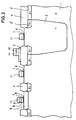
- Figs. 1 to 3 are partial sectional views of a silicon wafer during three separate stages of a method constituting an embodiment of the invention.
- The method initially comprises operations of conventional type for the manufacture of integrated circuits with complementary MOS transistors (CMOS). There are formed, in a substrate 1 of semiconductor material of a first type of conductivity (for instance p-doped monocrystalline silicon),
pockets 2 of opposite conductivity, i.e. n-doped, by appropriate masking, doping and diffusion operations. These pockets are designed to contain p-channel transistors. - A layer of inert material, typically silicon nitride, is then deposited and is masked and shaped to form the active areas, i.e. those areas designed to contain transistors and memory cells. By means of two successive masking stages, n-type and p-type doping ions are then implanted to increase the concentration of predetermined zones at the edges of the active areas for the formation of isolating or "channel stopper" regions.
- A high temperature (900-1000°C) operation is then carried out in an oxidizing atmosphere in order to grow the so-called field oxide, i.e. comparatively thick portions of silicon dioxide, shown at 4 in the drawings, only in the zones not covered by the silicon nitride. All the doping species contained in the structure are caused to diffuse so as to obtain p-
type isolating regions 3′, shown by p+, in the substrate p and n-type regions 3˝, shown by n+, in the pockets n (only one of which is shown in the drawings). - After the removal of the nitride layer, appropriate masking and implantation operations are carried out to increase the concentration of p-type doping agents in the active zones designed to contain EPROM memory cells, shown at 5 in the drawings. Oxidation is then carried out to grow a thin layer (for instance 150-500 A) of silicon dioxide on the active zones for the subsequent formation of the gate dielectric of the transistors and memory cells. A
polycrystalline silicon layer 7 is then deposited and doped and masking and etching operations are carried out to open up parallel slots in this layer in order to isolate the zones in which the memory cells are to be formed. - At this point, an
insulating layer 8, for instance of silicon dioxide, is formed by oxidation at high temperature and a thin layer (for instance 500 A) ofpolycrystalline silicon 9 is deposited thereon. - Successive masking and chemical etching operations are then carried out to remove the
polycrystalline silicon layer 9 and the underlyinginsulating layer 8 from the whole surface of the wafer with the exception of the zones destined for the memory cells. The wafer is then subjected to ion implantation with n-type impurities so as to increase the doping of thefirst layer 7 of polycrystalline silicon to increase its electrical conductivity and therefore make it suitable to form one of the electrodes of the capacitors. - An
insulating layer 10, for instance silicon dioxide obtained by vapour phase deposition by oxidation of tetraethylorthosilicate (TEOS) at approximately 700°C, is then formed and is removed by a masking and chemical etching operation from the whole of the wafer with the exception of predetermined areas above the field oxide. Thethin layer 9 of polycrystalline silicon is designed to shield the memory cell zones during the method stages specifically for the formation of the capacitors. - The method continues with the deposition of a
layer 11 of polycrystalline silicon and masking and chemical etching operations, until the structure shown in Fig. 2 is achieved. In the active areas intended for the memory cells, there are superimposed portions of the layer of silicon dioxide 6 (gate dielectric), the first polycrystalline silicon layer 7 (floating gate electrode), the insulating layer 8 ("interpoly" dielectric) and thelayers polycrystalline silicon layer 7 and the finalpolycrystalline silicon layer 11, the last two of which are shown separated by dashed lines but cannot in practice be distinguished from one another and together form the gate electrode of the transistors. In predetermined areas of the field oxide (only one of which is shown in the drawing), there are superimposed portions of the first polycrystalline silicon layer 7 (first electrode of the capacitor), the silicon dioxide layer 10 (capacitor dielectric) and the final layer of polycrystalline silicon 11 (second electrode of the capacitor). A capacitor structure of this type is disclosed for instance in the Italian Patent Application 23200 A/87 filed on 23 December 1987 in the name of SGS-Thomson Microelectronics S.p.A. - This is followed by subsequent conventional method steps comprising two successive masking operations for the implantation of ions of impurities of opposite type, followed by a high temperature treatment through which diffused source and drain regions are obtained in the active areas and, more particularly, n-type regions in the areas destined for the memory cells and the n-channel transistors, shown at 12 in Fig. 3, and p-type regions in the
pockets 2, shown at 13 in Fig. 3, i.e. in the areas destined for the p-channel transistors. - An insulating layer is then formed, windows are opened for contacts through this layer, a metal layer is deposited and is shaped by a masking operation to obtain the connections between the various components of the circuit. The structure shown in Fig. 3 is thus obtained, in which the
remaining portions 14 of the insulating layer and theremaining portions 15 of the metal layer for the connections are shown. Finally, the whole assembly is covered with an insulating protective layer (not shown) in which, by masking and chemical etching, windows are opened for connection of wire contacts externally to the integrated circuit. - The electrodes of the capacitors are formed using the same operations as are needed for the formation of the gate electrodes of the memory cells. However, the capacitors can be designed with optimum characteristics, since the doping of the polycrystalline silicon which forms the lower electrode can be determined independently of that of the polycrystalline silicon which forms the floating gate of the memory cells and the dielectric layer of the capacitors may have a thickness and physical characteristics differing from those of the "interpoly" dielectric of the memory cells since it is formed independently of the latter. Advantageously, dielectric may be formed by deposition at low temperature with the result that there is no detrimental effect on the doping profiles previously formed.
- This method consequently makes it possible to design and form the capacitors with extremely small dimensions and with considerable precision. Moreover, since this method does not require a third thick layer of polycrystalline silicon for the formation of the electrodes of the capacitors, the planar nature of the final surface is in practice equivalent to that which is obtained with conventional methods using two levels of polycrystalline silicon.
- Various modifications may be made within the scope of the invention. For instance, the insulating layer which forms the "interpoly" dielectric may be formed by superimposed layers of silicon dioxide, obtained by high temperature oxidation of the underlying
polycrystalline silicon layer 7, deposited silicon nitride and silicon dioxide obtained by oxidation of the underlying nitride. - Similarly, the dielectric 10 of the capacitors may be formed by superimposed layers of different materials, rather than by a single layer of silicon dioxide. Moreover, the method may be advantageously used both in CMOS manufacturing technology and in NMOS or PMOS manufacturing technology and in general in all cases in which it is desired to obtain electronic components comprising two electrodes separated by different dielectrics.
Claims (6)
- A method of making, on a substrate of semiconductor material, an integrated circuit comprising electronic components of two different types each having pairs of electrodes separated by dielectric material, comprising:
forming and doping a first polycrystalline silicon layer (7);
defining by masking and removal predetermined zones of the first polycrystalline silicon layer (7) on areas of the substrate previously covered with dielectric material (4, 6);
forming a first insulating layer (8) comprising at least one dielectric material on the first polycrystalline silicon layer (7);
forming a second polycrystalline silicon layer (9) on the first insulating layer (8);
masking at least one predetermined area of the second polycrystalline silicon layer (9), removing a portion of the second polycrystalline silicon layer (9) external to the or each predetermined area, and removing an underlying portion of the first insulating layer (8);
forming a second insulating layer (10) comprising at least one dielectric material on the first polycrystalline silicon layer (7);
masking at least one further predetermined area of the second insulating layer (10) and removing a portion of the second insulating layer (10) external to the or each further predetermined area;
forming a third polycrystalline silicon layer (11) at least on the or each predetermined area of the second polycrystalline silicon layer (9) and the or each further predetermined area of the second insulating layer (10); and
masking further predetermined zones of the third polycrystalline silicon layer (11) lying at least partially above the or each predetermined area and the or each further predetermined area and removing a portion of the third polycrystalline silicon layer (11) external to the further predetermined zones. - A method as claimed in Claim 1, characterized in that the first polycrystalline silicon layer (7) is subjected to a doping operation prior to the formation of the second insulating layer (10) thereon in order to increase its conductivity.
- A method as claimed in Claim 1 or 2, characterized in that the first insulating layer (8) is formed by:
oxidising the underlying first polycrystalline silicon layer (7);
depositing a layer of silicon nitride; and forming a layer of silicon dioxide. - A method as claimed in any one of the preceding claims, characterized in that the second insulating layer (10) is formed by oxidising tetraethylorthosilicate at a temperature of between 650 and 750°C.
- A method as claimed in any one of the preceding claims, characterised in that active zones for containing memory cells are defined on the areas of the substrate previously covered with dielectric material (4, 6).
- A method as claimed in any one of the preceding claims, characterised in that capacitors are formed in the or each further predetermined area.
Applications Claiming Priority (2)
| Application Number | Priority Date | Filing Date | Title |
|---|---|---|---|
| IT02268389A IT1237894B (en) | 1989-12-14 | 1989-12-14 | PROCESS FOR THE MANUFACTURE OF INTEGRATED CIRCUITS INCLUDING ELECTRONIC COMPONENTS OF TWO DIFFERENT TYPES HAVING EACH PAIR OF ELECTRODES RECOVERED FROM THE SAME LAYERS OF POLYCRYSTALLINE SILICON AND SEPARATED FROM DIFFERENT DIELECTRICS |
| IT2268389 | 1989-12-14 |
Publications (3)
| Publication Number | Publication Date |
|---|---|
| EP0435534A2 EP0435534A2 (en) | 1991-07-03 |
| EP0435534A3 EP0435534A3 (en) | 1991-11-06 |
| EP0435534B1 true EP0435534B1 (en) | 1995-11-08 |
Family
ID=11199229
Family Applications (1)
| Application Number | Title | Priority Date | Filing Date |
|---|---|---|---|
| EP90313667A Expired - Lifetime EP0435534B1 (en) | 1989-12-14 | 1990-12-14 | Method of manufacturing integrated circuit and integrated circuit made thereby |
Country Status (6)
| Country | Link |
|---|---|
| US (1) | US5075246A (en) |
| EP (1) | EP0435534B1 (en) |
| JP (1) | JP3199388B2 (en) |
| KR (1) | KR0179360B1 (en) |
| DE (1) | DE69023469T2 (en) |
| IT (1) | IT1237894B (en) |
Families Citing this family (13)
| Publication number | Priority date | Publication date | Assignee | Title |
|---|---|---|---|---|
| JPH05283710A (en) * | 1991-12-06 | 1993-10-29 | Intel Corp | High-voltage mos transistor and manufacture thereof |
| EP0557937A1 (en) * | 1992-02-25 | 1993-09-01 | Ramtron International Corporation | Ozone gas processing for ferroelectric memory circuits |
| US5340764A (en) * | 1993-02-19 | 1994-08-23 | Atmel Corporation | Integration of high performance submicron CMOS and dual-poly non-volatile memory devices using a third polysilicon layer |
| JPH06252345A (en) * | 1993-03-02 | 1994-09-09 | Nec Corp | Manufacture of semiconductor integrated circuit |
| US5550072A (en) * | 1994-08-30 | 1996-08-27 | National Semiconductor Corporation | Method of fabrication of integrated circuit chip containing EEPROM and capacitor |
| DE19531629C1 (en) * | 1995-08-28 | 1997-01-09 | Siemens Ag | Method of manufacturing an EEPROM semiconductor structure |
| JP3415712B2 (en) * | 1995-09-19 | 2003-06-09 | 松下電器産業株式会社 | Semiconductor device and manufacturing method thereof |
| RU2124252C1 (en) * | 1996-11-05 | 1998-12-27 | Агрич Юрий Владимирович | Cmos array chip manufacturing process |
| US5731236A (en) * | 1997-05-05 | 1998-03-24 | Taiwan Semiconductor Manufacturing Company, Ltd. | Process to integrate a self-aligned contact structure, with a capacitor structure |
| JP3556079B2 (en) * | 1997-10-02 | 2004-08-18 | 旭化成マイクロシステム株式会社 | Method for manufacturing semiconductor device |
| US6472259B1 (en) | 1999-04-01 | 2002-10-29 | Asahi Kasei Microsystems Co., Ltd. | Method of manufacturing semiconductor device |
| US8936838B2 (en) | 2012-01-16 | 2015-01-20 | Corning Incorporated | Method for coating polymers on glass edges |
| FR3059148B1 (en) * | 2016-11-23 | 2019-09-06 | Commissariat A L'energie Atomique Et Aux Energies Alternatives | REALIZING SELF-ALIGNED INTERCONNECTION ELEMENTS FOR INTEGRATED 3D CIRCUIT |
Family Cites Families (9)
| Publication number | Priority date | Publication date | Assignee | Title |
|---|---|---|---|---|
| US4441249A (en) * | 1982-05-26 | 1984-04-10 | Bell Telephone Laboratories, Incorporated | Semiconductor integrated circuit capacitor |
| US4536947A (en) * | 1983-07-14 | 1985-08-27 | Intel Corporation | CMOS process for fabricating integrated circuits, particularly dynamic memory cells with storage capacitors |
| US4639274A (en) * | 1984-11-28 | 1987-01-27 | Fairchild Semiconductor Corporation | Method of making precision high-value MOS capacitors |
| JPS61183952A (en) * | 1985-02-09 | 1986-08-16 | Fujitsu Ltd | Semiconductor memory device and manufacture thereof |
| US4971924A (en) * | 1985-05-01 | 1990-11-20 | Texas Instruments Incorporated | Metal plate capacitor and method for making the same |
| FR2583920B1 (en) * | 1985-06-21 | 1987-07-31 | Commissariat Energie Atomique | METHOD FOR MANUFACTURING AN INTEGRATED CIRCUIT, ESPECIALLY AN EPROM MEMORY COMPRISING TWO DISTINCT ELECTRICALLY ISOLATED COMPONENTS |
| IT1208646B (en) * | 1987-06-11 | 1989-07-10 | Sgs Mocroelettronica S P A | MASKING STAGES. PROCEDURE FOR THE MANUFACTURE OF CAPACITORS IN CMOS AND NMOS PROCESSES WITH REDUCTION OF THE NUMBER OF |
| IT1224656B (en) * | 1987-12-23 | 1990-10-18 | Sgs Thomson Microelectronics | PROCEDURE FOR THE MANUFACTURE OF CAPACITORS INTEGRATED IN MOS TECHNOLOGY. |
| FR2642900B1 (en) * | 1989-01-17 | 1991-05-10 | Sgs Thomson Microelectronics | METHOD FOR MANUFACTURING INTEGRATED CIRCUITS WITH EPROM MEMORY TRANSISTORS AND LOGIC TRANSISTORS |
-
1989
- 1989-12-14 IT IT02268389A patent/IT1237894B/en active IP Right Grant
-
1990
- 1990-12-11 JP JP40965490A patent/JP3199388B2/en not_active Expired - Fee Related
- 1990-12-12 KR KR1019900020410A patent/KR0179360B1/en not_active Expired - Fee Related
- 1990-12-13 US US07/625,764 patent/US5075246A/en not_active Expired - Lifetime
- 1990-12-14 DE DE69023469T patent/DE69023469T2/en not_active Expired - Fee Related
- 1990-12-14 EP EP90313667A patent/EP0435534B1/en not_active Expired - Lifetime
Also Published As
| Publication number | Publication date |
|---|---|
| US5075246A (en) | 1991-12-24 |
| KR910013571A (en) | 1991-08-08 |
| KR0179360B1 (en) | 1999-03-20 |
| EP0435534A2 (en) | 1991-07-03 |
| IT8922683A0 (en) | 1989-12-14 |
| EP0435534A3 (en) | 1991-11-06 |
| DE69023469D1 (en) | 1995-12-14 |
| JPH04119666A (en) | 1992-04-21 |
| IT1237894B (en) | 1993-06-18 |
| IT8922683A1 (en) | 1991-06-14 |
| DE69023469T2 (en) | 1996-05-02 |
| JP3199388B2 (en) | 2001-08-20 |
Similar Documents
| Publication | Publication Date | Title |
|---|---|---|
| EP0827634B1 (en) | Floating gate non-volatile memory device, and a method of manufacturing the device | |
| US5242851A (en) | Programmable interconnect device and method of manufacturing same | |
| US5920779A (en) | Differential gate oxide thickness by nitrogen implantation for mixed mode and embedded VLSI circuits | |
| US5013674A (en) | A method of manufacturing integrated circuits comprising EPROM memory and logic transistors | |
| EP0764986A1 (en) | Semiconductor device and method for manufacturing the same | |
| US5153143A (en) | Method of manufacturing CMOS integrated circuit with EEPROM | |
| US5075246A (en) | Method of manufacturing integrated circuits having electronic components of two different types each having pairs of electrodes obtained from the same polycrystalline silicon layers and separated by different dielectric materials | |
| JPH11511297A (en) | Method of manufacturing EEPROM semiconductor structure | |
| EP0135243B1 (en) | A method of producing a semiconductor structure on a substrate and a semiconductor device manufactured thereby | |
| JPH05251555A (en) | Manufacture of mos integrated circuit | |
| US4358889A (en) | Process for making a late programming enhanced contact ROM | |
| US5340764A (en) | Integration of high performance submicron CMOS and dual-poly non-volatile memory devices using a third polysilicon layer | |
| US5597753A (en) | CVD oxide coding method for ultra-high density mask read-only-memory (ROM) | |
| KR0172116B1 (en) | Manufacturing Method of Semiconductor Device | |
| US5650346A (en) | Method of forming MOSFET devices with buried bitline capacitors | |
| EP0716454A2 (en) | MOSFET device formed in epitaxial layer | |
| KR100951272B1 (en) | Manufacturing Method of Semiconductor Integrated Circuit Device | |
| WO1981002493A1 (en) | Self-aligned buried contact and method of making | |
| EP0880165B1 (en) | A method of manufacturing an integrated circuit with MOS transistors having high breakdown voltages, and with precision resistors | |
| US5977598A (en) | High load resistance implemented in a separate polysilicon layer with diffusion barrier therein for preventing load punch through therefrom | |
| EP0321860A2 (en) | Process for manufacturing integrated capacitors in mos technology | |
| US7294548B2 (en) | Semiconductor device and fabricating method thereof | |
| US5343062A (en) | Semiconductor memory having a memory cell including a capacitor with a two-layer lower electrode | |
| US6645817B2 (en) | Method of manufacturing a semiconductor device comprising MOS-transistors having gate oxides of different thicknesses | |
| GB2327810A (en) | Manufacturing integrated circuit devices with different gate oxide thicknesses |
Legal Events
| Date | Code | Title | Description |
|---|---|---|---|
| PUAI | Public reference made under article 153(3) epc to a published international application that has entered the european phase |
Free format text: ORIGINAL CODE: 0009012 |
|
| AK | Designated contracting states |
Kind code of ref document: A2 Designated state(s): DE FR GB SE |
|
| PUAL | Search report despatched |
Free format text: ORIGINAL CODE: 0009013 |
|
| AK | Designated contracting states |
Kind code of ref document: A3 Designated state(s): DE FR GB SE |
|
| RHK1 | Main classification (correction) |
Ipc: H01L 21/82 |
|
| 17P | Request for examination filed |
Effective date: 19910924 |
|
| 17Q | First examination report despatched |
Effective date: 19940328 |
|
| GRAA | (expected) grant |
Free format text: ORIGINAL CODE: 0009210 |
|
| AK | Designated contracting states |
Kind code of ref document: B1 Designated state(s): DE FR GB SE |
|
| REF | Corresponds to: |
Ref document number: 69023469 Country of ref document: DE Date of ref document: 19951214 |
|
| ET | Fr: translation filed | ||
| PG25 | Lapsed in a contracting state [announced via postgrant information from national office to epo] |
Ref country code: SE Effective date: 19960208 |
|
| PLBE | No opposition filed within time limit |
Free format text: ORIGINAL CODE: 0009261 |
|
| STAA | Information on the status of an ep patent application or granted ep patent |
Free format text: STATUS: NO OPPOSITION FILED WITHIN TIME LIMIT |
|
| 26N | No opposition filed | ||
| REG | Reference to a national code |
Ref country code: FR Ref legal event code: D6 |
|
| REG | Reference to a national code |
Ref country code: GB Ref legal event code: IF02 |
|
| PGFP | Annual fee paid to national office [announced via postgrant information from national office to epo] |
Ref country code: FR Payment date: 20021210 Year of fee payment: 13 |
|
| PGFP | Annual fee paid to national office [announced via postgrant information from national office to epo] |
Ref country code: GB Payment date: 20021211 Year of fee payment: 13 |
|
| PGFP | Annual fee paid to national office [announced via postgrant information from national office to epo] |
Ref country code: DE Payment date: 20021219 Year of fee payment: 13 |
|
| PG25 | Lapsed in a contracting state [announced via postgrant information from national office to epo] |
Ref country code: GB Free format text: LAPSE BECAUSE OF NON-PAYMENT OF DUE FEES Effective date: 20031214 |
|
| PG25 | Lapsed in a contracting state [announced via postgrant information from national office to epo] |
Ref country code: DE Free format text: LAPSE BECAUSE OF NON-PAYMENT OF DUE FEES Effective date: 20040701 |
|
| GBPC | Gb: european patent ceased through non-payment of renewal fee |
Effective date: 20031214 |
|
| PG25 | Lapsed in a contracting state [announced via postgrant information from national office to epo] |
Ref country code: FR Free format text: LAPSE BECAUSE OF NON-PAYMENT OF DUE FEES Effective date: 20040831 |
|
| REG | Reference to a national code |
Ref country code: FR Ref legal event code: ST |