EP0435404B1 - Differential input bicmos buffer-inverters and gates - Google Patents
Differential input bicmos buffer-inverters and gates Download PDFInfo
- Publication number
- EP0435404B1 EP0435404B1 EP90203439A EP90203439A EP0435404B1 EP 0435404 B1 EP0435404 B1 EP 0435404B1 EP 90203439 A EP90203439 A EP 90203439A EP 90203439 A EP90203439 A EP 90203439A EP 0435404 B1 EP0435404 B1 EP 0435404B1
- Authority
- EP
- European Patent Office
- Prior art keywords
- coupled
- transistor
- bipolar
- mos
- type
- Prior art date
- Legal status (The legal status is an assumption and is not a legal conclusion. Google has not performed a legal analysis and makes no representation as to the accuracy of the status listed.)
- Expired - Lifetime
Links
- 230000000295 complement effect Effects 0.000 claims description 29
- 239000000872 buffer Substances 0.000 description 30
- 230000006870 function Effects 0.000 description 8
- 238000010586 diagram Methods 0.000 description 5
- 230000015556 catabolic process Effects 0.000 description 1
- 230000003247 decreasing effect Effects 0.000 description 1
- 238000006731 degradation reaction Methods 0.000 description 1
- 238000005516 engineering process Methods 0.000 description 1
- 230000005669 field effect Effects 0.000 description 1
- 230000010354 integration Effects 0.000 description 1
- 238000000034 method Methods 0.000 description 1
- 238000012986 modification Methods 0.000 description 1
- 230000004048 modification Effects 0.000 description 1
- 230000000750 progressive effect Effects 0.000 description 1
- 230000003068 static effect Effects 0.000 description 1
- 238000006467 substitution reaction Methods 0.000 description 1
- 230000001360 synchronised effect Effects 0.000 description 1
Images


Classifications
-
- H—ELECTRICITY
- H03—ELECTRONIC CIRCUITRY
- H03K—PULSE TECHNIQUE
- H03K19/00—Logic circuits, i.e. having at least two inputs acting on one output; Inverting circuits
- H03K19/02—Logic circuits, i.e. having at least two inputs acting on one output; Inverting circuits using specified components
- H03K19/08—Logic circuits, i.e. having at least two inputs acting on one output; Inverting circuits using specified components using semiconductor devices
- H03K19/094—Logic circuits, i.e. having at least two inputs acting on one output; Inverting circuits using specified components using semiconductor devices using field-effect transistors
- H03K19/0944—Logic circuits, i.e. having at least two inputs acting on one output; Inverting circuits using specified components using semiconductor devices using field-effect transistors using MOSFET or insulated gate field-effect transistors, i.e. IGFET
- H03K19/09448—Logic circuits, i.e. having at least two inputs acting on one output; Inverting circuits using specified components using semiconductor devices using field-effect transistors using MOSFET or insulated gate field-effect transistors, i.e. IGFET in combination with bipolar transistors [BIMOS]
-
- H—ELECTRICITY
- H03—ELECTRONIC CIRCUITRY
- H03K—PULSE TECHNIQUE
- H03K19/00—Logic circuits, i.e. having at least two inputs acting on one output; Inverting circuits
-
- H—ELECTRICITY
- H03—ELECTRONIC CIRCUITRY
- H03K—PULSE TECHNIQUE
- H03K19/00—Logic circuits, i.e. having at least two inputs acting on one output; Inverting circuits
- H03K19/0175—Coupling arrangements; Interface arrangements
- H03K19/017509—Interface arrangements
- H03K19/017518—Interface arrangements using a combination of bipolar and field effect transistors [BIFET]
- H03K19/017527—Interface arrangements using a combination of bipolar and field effect transistors [BIFET] with at least one differential stage
-
- H—ELECTRICITY
- H03—ELECTRONIC CIRCUITRY
- H03K—PULSE TECHNIQUE
- H03K19/00—Logic circuits, i.e. having at least two inputs acting on one output; Inverting circuits
- H03K19/02—Logic circuits, i.e. having at least two inputs acting on one output; Inverting circuits using specified components
- H03K19/08—Logic circuits, i.e. having at least two inputs acting on one output; Inverting circuits using specified components using semiconductor devices
-
- H—ELECTRICITY
- H03—ELECTRONIC CIRCUITRY
- H03K—PULSE TECHNIQUE
- H03K19/00—Logic circuits, i.e. having at least two inputs acting on one output; Inverting circuits
- H03K19/20—Logic circuits, i.e. having at least two inputs acting on one output; Inverting circuits characterised by logic function, e.g. AND, OR, NOR, NOT circuits
Definitions
- BIOS Bipolar transistors and FETs
- MOSFETs or other types of IGFETs regardless of whether MOSFETs or other types of IGFETs are used or whether both p-channel and n-channel type MOS transistors are utilized in a single circuit.
- any description of a transistor as a MOS transistor is intended to be understood in its broadest sense to include other types of IGFETs and not to be limited to metalgate FETs.
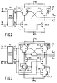
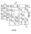
- OR gate 410a includes a bipolar transistor 491a, and two nMOS transistors 493a and 495a.
- Bipolar transistor 491a is coupled in parallel with transistor 420a, except that its base is coupled to the noninverting input V inb of a second complementary input.
- MOS transistor 493a is provided with its gate electrode coupled to the inverting input V inb , and with a drain coupled to the emitter of transistor 420a (via transistor 422a) and a source coupled to the drain of MOS transistor 424a.
- MOS transistor 495a is coupled in parallel with MOS transistor 424a, except that its gate is coupled to the noninverting V inb input.
Landscapes
- Engineering & Computer Science (AREA)
- Computer Hardware Design (AREA)
- Physics & Mathematics (AREA)
- Computing Systems (AREA)
- General Engineering & Computer Science (AREA)
- Mathematical Physics (AREA)
- Power Engineering (AREA)
- Logic Circuits (AREA)
- Electronic Switches (AREA)
- Amplifiers (AREA)
Description
Claims (14)
- An electronic circuit comprising: input means (311) with a first output terminal (Vin) for providing a first logic output signal (Vin), and a second output terminal (
V in) for providing a second logic output signal (V in), the first and the second logic output signals (Vin,V in) being complementary; a first bipolar transistor (320-1) having a base coupled to the first output terminal (Vin) of the input means (311), a collector coupled to a first voltage reference rail (VHH), and an emitter; a second bipolar transistor (328-1), having a collector coupled to the emitter of the first bipolar transistor (320-1), an emitter coupled to a second voltage reference rail (VLL), and an base; a first MOS transistor (322-1), having a drain, a source coupled to the base of the second bipolar transistor (328-1), and a gate coupled to the second output terminal (V in) of the input means (311), characterized in that the input means (311) further comprises a first input terminal (Vo) for receiving a first logic input signal (Vo) and a second input terminal (V o) for receiving a second logic input signal (V o), the first and the second logic input signals (Vo,V o) being complementary. - A circuit as in claim 1, characterized in that the drain of the first MOS transistor (322-1) is coupled to the emitter of the first bipolar transistor (320-1).
- A circuit as in claim 2, further comprising:a third bipolar transistor (320-2) having a base coupled for the second output terminal (
V in), a collector coupled to the first rail (VHH), and an emitter;a fourth bipolar transistor (328-2) having a base, a collector coupled to the emitter of the third bipolar transistor (320-2), and an emitter coupled to the second rail (VLL);a second MOS transistor (322-2) having a gate electrode coupled to the first output terminal (Vin), a drain coupled to the emitter of the third bipolar transistor (320-2), and a source coupled to the base of the fourth bipolar transistor (328-2), the first and second MOS transistors being of a first MOS type;a third MOS transistor (361-1), having a gate electrode coupled to an inventing output terminal (V out) of the electric circuit, a source coupled to the first rail (VHH), and a drain coupled to the emitter of the first bipolar transistor (320-1); anda fourth MOS transistor (361-2) having a gate electrode coupled to a noninventing output terminal (Vout) of the electric circuit, a source coupled to the first rail (VHH), and a drain coupled to the emitter of the third bipolar transistor (320-2), the third and fourth MOS transistors being of a second MOS type opposite to the first MOS type, the noninventing output terminal (Vout) and the inventing output terminal (V out) of the electronic circuit being coupled respectively for the emitters of the first (320-1) and third bipolar transistors. - A circuit as in claim 3 wherein the bipolar transistors (320-1, 320-2, 328-1, 328-2) are of a first bipolar type, the first MOS type is nMOS when the first bipolar type is npn, and the first MOS type is pMOS when the first bipolar type is pnp.
- A circuit as in claim 4 further comprising:a fifth MOS transistor (324-1) having a gate electrode responsive to the noninverting input (V0), a drain coupled to the source of the first MOS transistor (322-1), and a source coupled to the second rail (VLL); anda sixth MOS transistor (324-2) having a gate coupled to the first output terminal (Vin), a drain coupled to the source of the second MOS transistor (322-2), and a source coupled to the second rail (VLL), the fifth and sixth MOS transistors being of the first MOS type.
- A circuit as in claim 5, characterized in that the gate of the third MOS transistor (361-1) is coupled to the source of the third bipolar transistor (320-2), the gate of the fourth MOS-transistor (361-2) is coupled to the source of the first bipolar transistor (320-1), the gates of the first (322-1) and the sixth (324-2) MOS transistors are coupled to the base of the third bipolar transistor (320-2); and the gates of the third (322-2) and the fifth (324-1) MOS transistors are coupled to the base of the first bipolar transistor (320-1).
- A circuit as in claim 6 wherein the bipolar transistors (320-1, 320-2, 328-1, 328-2) are of a first bipolar type, the first MOS type is nMOS when the first bipolar type is npn, and the first MOS type is pMOS when the first bipolar type is pnp.
- A circuit as in claim 1 comprising: second input means (411aB) with a third output terminal (Vinb) for providing a third logic output signal (Vinb), and a fourth output terminal (
V inb) for providing a fourth logic output signal (V inb), the third and the fourth logic output signals (Vinb,V inb) being complementary; a third input terminal (Vob) for receiving a third logic input signal (Vob) and a fourth input terminal (V ob) for receiving a fourth logic input signal (V o), the third and the fourth logic input signals (Vob,V ob) being complementary; a noninverting output (Vout) coupled to the emitter of the first bipolar transistor (420a); a third bipolar transistor (491a) having a base coupled to the third output terminal (Vinb), a collector coupled to the collector of the first bipolar transistor (420a), and an emitter coupled to the emitter of the first bipolar transistor (420a); a second MOS transistor (422a) having a gate coupled to the second output terminal (V ina), a drain coupled to the emitter of the first bipolar transistor (420a), and a source; and that the gate of the first MOS transistor (493a) is coupled to the fourth output terminal (V inb), and the drain of the first MOS transistor (493a) is coupled to the source of the second MOS transistor (422a). - A circuit as in claim 8 further comprising:a third MOS transistor (424a) having a gate electrode coupled to the first noninverting output terminal (Vina) input (Voa), a drain coupled to the base of the second bipolar transistor (428a), and a source coupled to the second rail (VLL); anda fourth MOS transistor (495a) having a gate electrode coupled to the third output terminal (Vinb), a drain coupled to the base of the second bipolar transistor (428a), and a source coupled to the second rail (VLL).
- A circuit as in claim 9 wherein the MOS transistors (422a, 493a, 424a, 495a) are all of a first MOS type, the bipolar transistors (420a, 491a, 428a) are of a first bipolar type, the first MOS type is nMOS when the first bipolar type is npn, and the first MOS type is pMOS when the first bipolar type is pnp.
- A circuit as in claim 9 further comprising:a fourth bipolar transistor (420b-2) having a base coupled to the second output terminal (
V ina), a collector coupled to the second rail (VLL), and an emitter coupled to the inventing output terminal (V out)a fifth bipolar transistor (491b-2) having a base coupled to the fourth output terminal (V inb), a collector coupled to the second rail (VLL), and an emitter coupled to the emitter of the fourth bipolar transistor (420b-2).a sixth bipolar transistor (428b-2) a base, a collector, coupled to the emitter of the fourth bipolar transistor (420b-2), and an emitter coupled to the first rail (VHH);a fifth MOS transistor (422b-2) having a gate electrode coupled to the first output terminal (Vina), a drain, and a source;a sixth MOS transistor (493b-2) having a gate electrode coupled to the third output terminal (Vinb), a drain, and a source, the two MOS transistors (422b-2, 493b-2) being arranged in series such that the drain and the source of one are respectively coupled to the emitter of the fourth bipolar transistor (420b-2) and to the drain of the other whose source is coupled to the base of the third pnp transistor;a seventh MOS transistor (424b-2) having a gate electrode coupled to the second output terminal (V ina), a drain coupled to the base of the sixth bipolar transistor (428b-2), and a source coupled to the first rail (VHH); anda eighth MOS transistor (495b-2) having a gate electrode coupled to the fourth output terminal (V inb), a drain coupled to the base of the sixth bipolar transistor (428b-2), and a source coupled to the first rail (VHH). - A circuit as in claim 11 wherein the first (493b-1), the second (422b-1), the third (424b-1), and the fourth (495b-1) MOS transistors are of a first MOS type; the first (420b-1), the second (428b-1), and the third (491b-1) bipolar transistors are of a first bipolar type; the fifth (422b-2), the sixth (493b-2), the seventh (424b-2), and the eight (495b-2) MOS transistors are of a second MOS type; the fourth (420b-2), the fifth (491b-2), and the sixth (428b-2) bipolar transistors are of a second bipolar type; the first MOS type in nMOS when the first bipolar type is npn, and the first type is pMOS when the first bipolar type is pnp.
- A circuit as in claim 10 further comprising: circuitry being a duplicate of the circuitry constituted by the first (520a), the second (528a), and the third (591a) bipolar transistors; and the first (593a), the second (522a), the third (524a), and the fourth (595a) MOS transistors; a duplicated non inverting output terminal (Vout') coupled to the emitters of the corresponding bipolar transistors of the duplicated circuitry; and input terminals of the duplicated circuitry, with regard to the non duplicated circuitry, inversely responsive to the non inverting (Voa,Vob) and the inverting (
V oa,V ob) input terminals - A circuit as in claim 13 wherein the MOS transistors are all of a first MOS type, the bipolar transistors are of a first bipolar type, the first MOS type is nMOS when the first bipolar type is npn, and the first MOS type is pMOS when the first bipolar type is pMOS.
Applications Claiming Priority (2)
| Application Number | Priority Date | Filing Date | Title |
|---|---|---|---|
| US45821789A | 1989-12-28 | 1989-12-28 | |
| US458217 | 1989-12-28 |
Publications (3)
| Publication Number | Publication Date |
|---|---|
| EP0435404A2 EP0435404A2 (en) | 1991-07-03 |
| EP0435404A3 EP0435404A3 (en) | 1991-11-27 |
| EP0435404B1 true EP0435404B1 (en) | 2000-10-25 |
Family
ID=23819847
Family Applications (1)
| Application Number | Title | Priority Date | Filing Date |
|---|---|---|---|
| EP90203439A Expired - Lifetime EP0435404B1 (en) | 1989-12-28 | 1990-12-19 | Differential input bicmos buffer-inverters and gates |
Country Status (4)
| Country | Link |
|---|---|
| EP (1) | EP0435404B1 (en) |
| JP (1) | JP3117223B2 (en) |
| KR (1) | KR100220112B1 (en) |
| DE (1) | DE69033654T2 (en) |
Cited By (1)
| Publication number | Priority date | Publication date | Assignee | Title |
|---|---|---|---|---|
| RU2526756C1 (en) * | 2013-01-22 | 2014-08-27 | Российская Федерация, от имени которой выступает Государственная корпорация по атомной энергии "Росатом" | Charge-sensitive preamplifier |
Citations (1)
| Publication number | Priority date | Publication date | Assignee | Title |
|---|---|---|---|---|
| EP0209805A2 (en) * | 1985-07-22 | 1987-01-28 | Hitachi, Ltd. | Semiconductor device having bipolar transistor and insulated gate field effect transistor |
Family Cites Families (2)
| Publication number | Priority date | Publication date | Assignee | Title |
|---|---|---|---|---|
| EP0058958B1 (en) * | 1981-02-25 | 1986-10-29 | Kabushiki Kaisha Toshiba | Complementary mosfet logic circuit |
| JPH02303216A (en) * | 1989-05-17 | 1990-12-17 | Fujitsu Ltd | Semiconductor integrated circuit |
-
1990
- 1990-12-19 EP EP90203439A patent/EP0435404B1/en not_active Expired - Lifetime
- 1990-12-19 DE DE69033654T patent/DE69033654T2/en not_active Expired - Lifetime
- 1990-12-25 JP JP02419109A patent/JP3117223B2/en not_active Expired - Lifetime
- 1990-12-28 KR KR1019900022214A patent/KR100220112B1/en not_active Expired - Lifetime
Patent Citations (1)
| Publication number | Priority date | Publication date | Assignee | Title |
|---|---|---|---|---|
| EP0209805A2 (en) * | 1985-07-22 | 1987-01-28 | Hitachi, Ltd. | Semiconductor device having bipolar transistor and insulated gate field effect transistor |
Cited By (1)
| Publication number | Priority date | Publication date | Assignee | Title |
|---|---|---|---|---|
| RU2526756C1 (en) * | 2013-01-22 | 2014-08-27 | Российская Федерация, от имени которой выступает Государственная корпорация по атомной энергии "Росатом" | Charge-sensitive preamplifier |
Also Published As
| Publication number | Publication date |
|---|---|
| JPH04280114A (en) | 1992-10-06 |
| KR100220112B1 (en) | 1999-09-01 |
| EP0435404A3 (en) | 1991-11-27 |
| EP0435404A2 (en) | 1991-07-03 |
| KR910013737A (en) | 1991-08-08 |
| JP3117223B2 (en) | 2000-12-11 |
| DE69033654D1 (en) | 2000-11-30 |
| DE69033654T2 (en) | 2001-05-10 |
Similar Documents
| Publication | Publication Date | Title |
|---|---|---|
| US5250856A (en) | Differential input buffer-inverters and gates | |
| US4703203A (en) | BICMOS logic having three state output | |
| US5204557A (en) | Digital signal level translator | |
| US6133753A (en) | Tri-state input detection circuit | |
| CA1206535A (en) | Interface circuit | |
| KR100290725B1 (en) | Emitter coupled logic-bipolar complementary metal oxide semiconductor / complementary metal oxide semiconductor translators | |
| US5103116A (en) | CMOS single phase registers | |
| WO1985002957A1 (en) | Complementary field effect transistor "exclusive or" (or "nor") logic gates | |
| EP0110060B1 (en) | Fet voltage level shift circuitry | |
| KR19990063442A (en) | Voltage conversion buffer circuit | |
| KR100499816B1 (en) | Synchronous Semiconductor Logic Circuit | |
| US5155387A (en) | Circuit suitable for differential multiplexers and logic gates utilizing bipolar and field-effect transistors | |
| US5173624A (en) | Level-shifter circuit for high-speed low-power bicmos ecl to cmos input buffers | |
| US4725982A (en) | Tri-state buffer circuit | |
| US6211721B1 (en) | Multiplexer with short propagation delay and low power consumption | |
| US6310509B1 (en) | Differential multiplexer with high bandwidth and reduced crosstalk | |
| US4943740A (en) | Ultra fast logic | |
| US5043602A (en) | High speed logic circuit with reduced quiescent current | |
| JP2865256B2 (en) | Bipolar / MOS logic circuit | |
| US4897567A (en) | Fast level translator circuit | |
| US5311075A (en) | Level shifting CMOS integrated circuits | |
| US5945848A (en) | Effectively differential, multiple input OR/NOR gate architecture | |
| JP2534377B2 (en) | BICMOS logic circuit | |
| EP0435404A2 (en) | Differential input bicmos buffer-inverters and gates | |
| EP0435389B1 (en) | Differential input, differential output BICMOS multiplexers and logic gates and an adder utilizing the same |
Legal Events
| Date | Code | Title | Description |
|---|---|---|---|
| PUAI | Public reference made under article 153(3) epc to a published international application that has entered the european phase |
Free format text: ORIGINAL CODE: 0009012 |
|
| AK | Designated contracting states |
Kind code of ref document: A2 Designated state(s): DE FR GB IT |
|
| PUAL | Search report despatched |
Free format text: ORIGINAL CODE: 0009013 |
|
| AK | Designated contracting states |
Kind code of ref document: A3 Designated state(s): DE FR GB IT |
|
| 17P | Request for examination filed |
Effective date: 19920527 |
|
| 17Q | First examination report despatched |
Effective date: 19960227 |
|
| RAP3 | Party data changed (applicant data changed or rights of an application transferred) |
Owner name: KONINKLIJKE PHILIPS ELECTRONICS N.V. |
|
| GRAG | Despatch of communication of intention to grant |
Free format text: ORIGINAL CODE: EPIDOS AGRA |
|
| 17Q | First examination report despatched |
Effective date: 19960227 |
|
| GRAG | Despatch of communication of intention to grant |
Free format text: ORIGINAL CODE: EPIDOS AGRA |
|
| GRAH | Despatch of communication of intention to grant a patent |
Free format text: ORIGINAL CODE: EPIDOS IGRA |
|
| GRAH | Despatch of communication of intention to grant a patent |
Free format text: ORIGINAL CODE: EPIDOS IGRA |
|
| GRAA | (expected) grant |
Free format text: ORIGINAL CODE: 0009210 |
|
| AK | Designated contracting states |
Kind code of ref document: B1 Designated state(s): DE FR GB IT |
|
| PG25 | Lapsed in a contracting state [announced via postgrant information from national office to epo] |
Ref country code: IT Free format text: LAPSE BECAUSE OF FAILURE TO SUBMIT A TRANSLATION OF THE DESCRIPTION OR TO PAY THE FEE WITHIN THE PRE;WARNING: LAPSES OF ITALIAN PATENTS WITH EFFECTIVE DATE BEFORE 2007 MAY HAVE OCCURRED AT ANY TIME BEFORE 2007. THE CORRECT EFFECTIVE DATE MAY BE DIFFERENT FROM THE ONE RECORDED.SCRIBED TIME-LIMIT Effective date: 20001025 |
|
| REF | Corresponds to: |
Ref document number: 69033654 Country of ref document: DE Date of ref document: 20001130 |
|
| ET | Fr: translation filed | ||
| PLBE | No opposition filed within time limit |
Free format text: ORIGINAL CODE: 0009261 |
|
| STAA | Information on the status of an ep patent application or granted ep patent |
Free format text: STATUS: NO OPPOSITION FILED WITHIN TIME LIMIT |
|
| 26N | No opposition filed | ||
| REG | Reference to a national code |
Ref country code: GB Ref legal event code: IF02 |
|
| REG | Reference to a national code |
Ref country code: GB Ref legal event code: 746 Effective date: 20020918 |
|
| REG | Reference to a national code |
Ref country code: FR Ref legal event code: D6 |
|
| REG | Reference to a national code |
Ref country code: GB Ref legal event code: 732E |
|
| REG | Reference to a national code |
Ref country code: GB Ref legal event code: 732E |
|
| REG | Reference to a national code |
Ref country code: FR Ref legal event code: TP |
|
| REG | Reference to a national code |
Ref country code: FR Ref legal event code: GC |
|
| REG | Reference to a national code |
Ref country code: FR Ref legal event code: GC |
|
| PGFP | Annual fee paid to national office [announced via postgrant information from national office to epo] |
Ref country code: GB Payment date: 20091216 Year of fee payment: 20 Ref country code: FR Payment date: 20091221 Year of fee payment: 20 |
|
| PGFP | Annual fee paid to national office [announced via postgrant information from national office to epo] |
Ref country code: DE Payment date: 20091217 Year of fee payment: 20 |
|
| REG | Reference to a national code |
Ref country code: GB Ref legal event code: PE20 Expiry date: 20101218 |
|
| PG25 | Lapsed in a contracting state [announced via postgrant information from national office to epo] |
Ref country code: GB Free format text: LAPSE BECAUSE OF EXPIRATION OF PROTECTION Effective date: 20101218 |
|
| PG25 | Lapsed in a contracting state [announced via postgrant information from national office to epo] |
Ref country code: DE Free format text: LAPSE BECAUSE OF EXPIRATION OF PROTECTION Effective date: 20101219 |