EP0434075B1 - Vertical yoke protection system - Google Patents
Vertical yoke protection system Download PDFInfo
- Publication number
- EP0434075B1 EP0434075B1 EP90125018A EP90125018A EP0434075B1 EP 0434075 B1 EP0434075 B1 EP 0434075B1 EP 90125018 A EP90125018 A EP 90125018A EP 90125018 A EP90125018 A EP 90125018A EP 0434075 B1 EP0434075 B1 EP 0434075B1
- Authority
- EP
- European Patent Office
- Prior art keywords
- vertical
- circuit
- yoke
- vertical yoke
- protection arrangement
- Prior art date
- Legal status (The legal status is an assumption and is not a legal conclusion. Google has not performed a legal analysis and makes no representation as to the accuracy of the status listed.)
- Expired - Lifetime
Links
- 239000003990 capacitor Substances 0.000 claims description 36
- 238000005070 sampling Methods 0.000 claims description 13
- 238000007493 shaping process Methods 0.000 claims description 8
- 230000008878 coupling Effects 0.000 claims description 2
- 238000010168 coupling process Methods 0.000 claims description 2
- 238000005859 coupling reaction Methods 0.000 claims description 2
- 238000010586 diagram Methods 0.000 description 8
- 230000000903 blocking effect Effects 0.000 description 6
- 102100037460 E3 ubiquitin-protein ligase Topors Human genes 0.000 description 4
- 101000662670 Homo sapiens E3 ubiquitin-protein ligase Topors Proteins 0.000 description 4
- 101000772173 Homo sapiens Tubby-related protein 1 Proteins 0.000 description 3
- -1 RP07 Proteins 0.000 description 3
- 101000677914 Saccharomyces cerevisiae (strain ATCC 204508 / S288c) 40S ribosomal protein S5 Proteins 0.000 description 3
- 102100029293 Tubby-related protein 1 Human genes 0.000 description 3
- 208000002905 retinitis pigmentosa 14 Diseases 0.000 description 3
- 101001105683 Homo sapiens Pre-mRNA-processing-splicing factor 8 Proteins 0.000 description 2
- 101000875616 Homo sapiens Protein FAM161A Proteins 0.000 description 2
- 101000610557 Homo sapiens U4/U6 small nuclear ribonucleoprotein Prp31 Proteins 0.000 description 2
- 101001104102 Homo sapiens X-linked retinitis pigmentosa GTPase regulator Proteins 0.000 description 2
- 102100021231 Pre-mRNA-processing-splicing factor 8 Human genes 0.000 description 2
- 102100036002 Protein FAM161A Human genes 0.000 description 2
- 101000862778 Saccharomyces cerevisiae (strain ATCC 204508 / S288c) 40S ribosomal protein S3 Proteins 0.000 description 2
- 101001105592 Saccharomyces cerevisiae (strain ATCC 204508 / S288c) 60S ribosomal protein L18-A Proteins 0.000 description 2
- 101001105589 Saccharomyces cerevisiae (strain ATCC 204508 / S288c) 60S ribosomal protein L18-B Proteins 0.000 description 2
- 101001109965 Saccharomyces cerevisiae (strain ATCC 204508 / S288c) 60S ribosomal protein L7-A Proteins 0.000 description 2
- 101001109960 Saccharomyces cerevisiae (strain ATCC 204508 / S288c) 60S ribosomal protein L7-B Proteins 0.000 description 2
- 102100040118 U4/U6 small nuclear ribonucleoprotein Prp31 Human genes 0.000 description 2
- 102100040092 X-linked retinitis pigmentosa GTPase regulator Human genes 0.000 description 2
- 230000001172 regenerating effect Effects 0.000 description 2
- 208000002909 retinitis pigmentosa 13 Diseases 0.000 description 2
- 201000010649 retinitis pigmentosa 28 Diseases 0.000 description 2
- 102100027518 1,25-dihydroxyvitamin D(3) 24-hydroxylase, mitochondrial Human genes 0.000 description 1
- 102100028359 ADP-ribosylation factor-like protein 6 Human genes 0.000 description 1
- 101100082481 Arabidopsis thaliana CEP1 gene Proteins 0.000 description 1
- 101100440894 Arabidopsis thaliana CP33 gene Proteins 0.000 description 1
- 102100022794 Bestrophin-1 Human genes 0.000 description 1
- 101000849787 Brucella melitensis biotype 1 (strain 16M / ATCC 23456 / NCTC 10094) Ribosome-recycling factor Proteins 0.000 description 1
- 102100035344 Cadherin-related family member 1 Human genes 0.000 description 1
- 102100031060 Clarin-1 Human genes 0.000 description 1
- 102100037364 Craniofacial development protein 1 Human genes 0.000 description 1
- 102100039282 Cytochrome P450 26A1 Human genes 0.000 description 1
- 102100039208 Cytochrome P450 3A5 Human genes 0.000 description 1
- 102100036511 Dehydrodolichyl diphosphate synthase complex subunit DHDDS Human genes 0.000 description 1
- 102100033968 Guanylyl cyclase-activating protein 2 Human genes 0.000 description 1
- 101000861278 Homo sapiens 1,25-dihydroxyvitamin D(3) 24-hydroxylase, mitochondrial Proteins 0.000 description 1
- 101000769028 Homo sapiens ADP-ribosylation factor-like protein 6 Proteins 0.000 description 1
- 101000903449 Homo sapiens Bestrophin-1 Proteins 0.000 description 1
- 101000737767 Homo sapiens Cadherin-related family member 1 Proteins 0.000 description 1
- 101000992973 Homo sapiens Clarin-1 Proteins 0.000 description 1
- 101000880187 Homo sapiens Craniofacial development protein 1 Proteins 0.000 description 1
- 101000745891 Homo sapiens Cytochrome P450 26A1 Proteins 0.000 description 1
- 101000745710 Homo sapiens Cytochrome P450 3A5 Proteins 0.000 description 1
- 101000928713 Homo sapiens Dehydrodolichyl diphosphate synthase complex subunit DHDDS Proteins 0.000 description 1
- 101001068475 Homo sapiens Guanylyl cyclase-activating protein 2 Proteins 0.000 description 1
- 101001033697 Homo sapiens Interphotoreceptor matrix proteoglycan 2 Proteins 0.000 description 1
- 101000721946 Homo sapiens Oral-facial-digital syndrome 1 protein Proteins 0.000 description 1
- 101001113706 Homo sapiens Photoreceptor cilium actin regulator Proteins 0.000 description 1
- 101000611618 Homo sapiens Photoreceptor disk component PRCD Proteins 0.000 description 1
- 101000633511 Homo sapiens Photoreceptor-specific nuclear receptor Proteins 0.000 description 1
- 101000610551 Homo sapiens Prominin-1 Proteins 0.000 description 1
- 101000726148 Homo sapiens Protein crumbs homolog 1 Proteins 0.000 description 1
- 101000742938 Homo sapiens Retinol dehydrogenase 12 Proteins 0.000 description 1
- 101000609947 Homo sapiens Rod cGMP-specific 3',5'-cyclic phosphodiesterase subunit alpha Proteins 0.000 description 1
- 101000875401 Homo sapiens Sterol 26-hydroxylase, mitochondrial Proteins 0.000 description 1
- 101000659545 Homo sapiens U5 small nuclear ribonucleoprotein 200 kDa helicase Proteins 0.000 description 1
- 102100039092 Interphotoreceptor matrix proteoglycan 2 Human genes 0.000 description 1
- 101000863415 Kluyveromyces lactis (strain ATCC 8585 / CBS 2359 / DSM 70799 / NBRC 1267 / NRRL Y-1140 / WM37) 40S ribosomal protein S14 Proteins 0.000 description 1
- 101710121003 Oxygen-evolving enhancer protein 3, chloroplastic Proteins 0.000 description 1
- 108090000709 Phakinin Proteins 0.000 description 1
- 102100035832 Phakinin Human genes 0.000 description 1
- 102100023739 Photoreceptor cilium actin regulator Human genes 0.000 description 1
- 102100040826 Photoreceptor disk component PRCD Human genes 0.000 description 1
- 102100029533 Photoreceptor-specific nuclear receptor Human genes 0.000 description 1
- 101710201952 Photosystem II 22 kDa protein, chloroplastic Proteins 0.000 description 1
- 102100040120 Prominin-1 Human genes 0.000 description 1
- 102100027331 Protein crumbs homolog 1 Human genes 0.000 description 1
- 102100038054 Retinol dehydrogenase 12 Human genes 0.000 description 1
- 102100039177 Rod cGMP-specific 3',5'-cyclic phosphodiesterase subunit alpha Human genes 0.000 description 1
- 101000717877 Saccharomyces cerevisiae (strain ATCC 204508 / S288c) 40S ribosomal protein S11-A Proteins 0.000 description 1
- 101000717881 Saccharomyces cerevisiae (strain ATCC 204508 / S288c) 40S ribosomal protein S11-B Proteins 0.000 description 1
- 101000825534 Saccharomyces cerevisiae (strain ATCC 204508 / S288c) 40S ribosomal protein S2 Proteins 0.000 description 1
- 101001115232 Saccharomyces cerevisiae (strain ATCC 204508 / S288c) 40S ribosomal protein S22-A Proteins 0.000 description 1
- 101000811330 Saccharomyces cerevisiae (strain ATCC 204508 / S288c) 40S ribosomal protein S22-B Proteins 0.000 description 1
- 101000811350 Saccharomyces cerevisiae (strain ATCC 204508 / S288c) 40S ribosomal protein S23-A Proteins 0.000 description 1
- 101000811353 Saccharomyces cerevisiae (strain ATCC 204508 / S288c) 40S ribosomal protein S23-B Proteins 0.000 description 1
- 101000656770 Saccharomyces cerevisiae (strain ATCC 204508 / S288c) 40S ribosomal protein S24-A Proteins 0.000 description 1
- 101000656772 Saccharomyces cerevisiae (strain ATCC 204508 / S288c) 40S ribosomal protein S24-B Proteins 0.000 description 1
- 101000731924 Saccharomyces cerevisiae (strain ATCC 204508 / S288c) 40S ribosomal protein S27-A Proteins 0.000 description 1
- 101000731894 Saccharomyces cerevisiae (strain ATCC 204508 / S288c) 40S ribosomal protein S27-B Proteins 0.000 description 1
- 101000643078 Saccharomyces cerevisiae (strain ATCC 204508 / S288c) 40S ribosomal protein S9-A Proteins 0.000 description 1
- 101000729607 Saccharomyces cerevisiae (strain ATCC 204508 / S288c) 40S ribosomal protein S9-B Proteins 0.000 description 1
- 101000679737 Saccharomyces cerevisiae (strain ATCC 204508 / S288c) 60S ribosomal protein L16-B Proteins 0.000 description 1
- 101000751147 Saccharomyces cerevisiae (strain ATCC 204508 / S288c) 60S ribosomal protein L19-A Proteins 0.000 description 1
- 101000751149 Saccharomyces cerevisiae (strain ATCC 204508 / S288c) 60S ribosomal protein L19-B Proteins 0.000 description 1
- 102100021941 Sorcin Human genes 0.000 description 1
- 101000942680 Sus scrofa Clusterin Proteins 0.000 description 1
- 102100036230 U5 small nuclear ribonucleoprotein 200 kDa helicase Human genes 0.000 description 1
- 230000000712 assembly Effects 0.000 description 1
- 238000000429 assembly Methods 0.000 description 1
- 239000004020 conductor Substances 0.000 description 1
- 239000013078 crystal Substances 0.000 description 1
- 230000001351 cycling effect Effects 0.000 description 1
- 230000007423 decrease Effects 0.000 description 1
- 230000001419 dependent effect Effects 0.000 description 1
- 230000000694 effects Effects 0.000 description 1
- 238000009499 grossing Methods 0.000 description 1
- 238000010438 heat treatment Methods 0.000 description 1
- 238000000034 method Methods 0.000 description 1
- 208000006957 retinitis pigmentosa 29 Diseases 0.000 description 1
- 201000010648 retinitis pigmentosa 33 Diseases 0.000 description 1
- 208000006949 retinitis pigmentosa 35 Diseases 0.000 description 1
- 201000010358 retinitis pigmentosa 37 Diseases 0.000 description 1
- 201000010613 retinitis pigmentosa 41 Diseases 0.000 description 1
- 201000010361 retinitis pigmentosa 50 Diseases 0.000 description 1
- 201000010622 retinitis pigmentosa 55 Diseases 0.000 description 1
- 201000010621 retinitis pigmentosa 56 Diseases 0.000 description 1
- 201000010685 retinitis pigmentosa 59 Diseases 0.000 description 1
- 201000010579 retinitis pigmentosa 63 Diseases 0.000 description 1
- 108010071065 ribosomal protein 29 Proteins 0.000 description 1
- 238000006467 substitution reaction Methods 0.000 description 1
- 230000001052 transient effect Effects 0.000 description 1
Images




Classifications
-
- H—ELECTRICITY
- H04—ELECTRIC COMMUNICATION TECHNIQUE
- H04N—PICTORIAL COMMUNICATION, e.g. TELEVISION
- H04N3/00—Scanning details of television systems; Combination thereof with generation of supply voltages
- H04N3/10—Scanning details of television systems; Combination thereof with generation of supply voltages by means not exclusively optical-mechanical
- H04N3/16—Scanning details of television systems; Combination thereof with generation of supply voltages by means not exclusively optical-mechanical by deflecting electron beam in cathode-ray tube, e.g. scanning corrections
-
- H—ELECTRICITY
- H04—ELECTRIC COMMUNICATION TECHNIQUE
- H04N—PICTORIAL COMMUNICATION, e.g. TELEVISION
- H04N3/00—Scanning details of television systems; Combination thereof with generation of supply voltages
- H04N3/10—Scanning details of television systems; Combination thereof with generation of supply voltages by means not exclusively optical-mechanical
- H04N3/16—Scanning details of television systems; Combination thereof with generation of supply voltages by means not exclusively optical-mechanical by deflecting electron beam in cathode-ray tube, e.g. scanning corrections
- H04N3/20—Prevention of damage to cathode-ray tubes in the event of failure of scanning
Definitions
- This invention relates generally to the field of overcurrent protection systems, and more particularly, to the field of overcurrent protection circuits for vertical deflection circuits and associated vertical yoke circuits of television apparatus.
- Vertical yoke assemblies and associated components of a television receiver are designed to insure that safety hazards are substantially eliminated in the associated design.
- a vertical yoke assembly of a television receiver is connected in series with an S-shaping capacitor and a sampling resistor.
- the sampling resistor provides a vertical feedback voltage signal, between a source of high voltage and a reference potential, usually ground. It is important to insure that in the event the S-shaping capacitor is shorted, that the short circuit current flowing through the circuit does not become a safety hazard due to excess power or heat generated in the vertical yoke assembly.
- Overcurrent conditions in the vertical yoke can also result from faults, for example short circuits, in the vertical driver stage supplying the vertical deflection current to the yoke.
- a vertical yoke has a substantially higher impedance, typically 15 ohms, compared to that of a sampling resistor, which often has a resistance in the range of 2 to 3 ohms. Accordingly, most of the power generated by such a short circuit condition will be dissipated in the vertical yoke, rather than in the sampling resistor. None of the prior art attempts to correct this problem have been wholly satisfactory. Such attempts have included the use of fuses or fusible resistors in series with the vertical yoke assembly.
- Fusible resistors prove unsatisfactory in large measure because there is not enough power dissipated in the resistor to fuse the component and open the circuit path.
- the mere substitution of components having higher rated voltage or current ratings is often unsatisfactory for a number of reasons. Higher rated components are usually more expensive. Higher rated components such as capacitors, for example, are much larger. Moreover, a higher rated component able to withstand a higher voltage or current will likely only cause a different, lower rated component to fail in its place.
- the invention provides a practical protection circuit for the vertical yoke assembly of a television receiver, or similar such device.
- the invention provides a relatively inexpensive protection circuit for preventing damage to a vertical yoke assembly from overcurrent conditions caused by transient phenomena, or the occurrence of a short circuit in a vertical yoke assembly or in circuitry associated with the vertical yoke assembly.
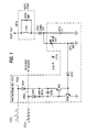
- FIGURE 1 is a circuit schematic diagram of an inventive arrangement of the invention.
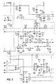
- FIGURE 2 is a circuit schematic diagram of a portion of a television receiver, showing a power supply, a sawtooth oscillator driver, a sawtooth oscillator, a portion of a gate circuit, and a portion of the protection circuit for one embodiment of the invention.
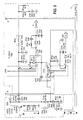
- FIGURE 3 is a circuit schematic diagram showing the remaining portion of the gate circuit of FIGURE 2, a horizontal driver circuit, and various other components of the illustrated television receiver, in this example.
- FIGURE 4 is a circuit schematic diagram of a portion of the flyback circuit for the illustrated television receiver.
- FIGURE 5 is a circuit schematic diagram showing the remaining portion of the flyback circuit, and the horizontal output stage for the illustrated television receiver.
- FIGURE 6 is a partial block diagram and circuit schematic diagram showing a control chip and associated circuitry for the illustrated television receiver.
- FIGURE 7 is a circuit schematic diagram showing the vertical output driver stage for the illustrated television receiver, and other portions of the illustrated embodiment of the invention.
- a typical vertical yoke assembly BF01 is an inductor LY01, and a resistor RY01 coupled in parallel with the inductor.
- An S-shaping capacitor CF01, and a sampling resistor RF01 are coupled in series with the inductor.
- a vertical feedback voltage is developed across the sampling resistor.
- the feedback voltage developed across resistor RF01 is AC coupled by capacitor CF02 to control circuitry of the television receiver, for providing a VFB (vertical feedback) signal thereto. If capacitor CF01 becomes short circuited, excessive current can flow through the vertical yoke assembly BF01 and resistor RF01.
- the vertical yoke assembly BF01 is protected from such overcurrent conditions according to an inventive arrangement.
- the voltage developed across the vertical feedback sampling resistor RF01 is also used for developing a signal indicative of the magnitude of current flowing through the yoke assembly BF01 at any given time.
- the vertical feedback voltage is divided down via the series circuit of potentiometer PF01 and resistor RF11, whereby the divided down voltage developed across resistor RF11 provides a signal proportional to the magnitude of current through the yoke assembly BF01.
- the vertical yoke overcurrent signal is coupled by a blocking diode DF01 to a regenerative switching circuit including NPN transistor TP08 and PNP transistor TP07.
- a speed-up capacitor CP06 is also included between the base and emitter electrodes of transistor TP07, and a shunt resistor RP28 across capacitor CP06.
- the emitter electrode transistor TP08 is connected to ground, and its base electrode is connected in common with the collector electrode of transistor TP07 to the cathode electrode of blocking diode DF01, the anode electrode of the latter being connected to one end of resistor RF11.
- a blocking diode DP07 has its cathode electrode connected to the common connection of the base and collector electrodes of transistors TP07 and TP08, respectively, with the anode electrode of diode DP07 being connected to a sawtooth signal line ST02, for a sawtooth signal ST03 generated by a sawtooth oscillator described below.
- Another blocking diode DP01 has an anode electrode connected to a power supply line or conductor PS02 along which half wave rectified voltages PS03 are conducted from a power supply described below.
- the cathode electrode of diode DP01 is connected to the emitter electrode of transistor TP07.
- resistor RF11 relative to that of potentiometer PF01, is such that for normal operation of the vertical yoke assembly, an insufficient level of voltage will be developed across potentiometer PF01 for forward biasing diode DF01 and for turning on transistors TP08 and TP07.
- the voltage developed across resistor RF11 will exceed a predetermined value, causing transistor TP08 to turn on, in turn turning on transistor TP07 in a regenerative manner, as is known in the art.
- Transistors TP07 and TP08 will remain turned on or latched until such time that the magnitude of current through their respective collector and emitter electrode current paths decreases to below a sustaining value.
- the voltage line PS02 when transistor TP07 so turns on, the voltage line PS02 is about three diode drops above ground, and the sawtooth voltage line ST02 is about two diode drops above ground.
- Substantial grounding of voltage line PS02 prevents the half wave rectified signals PS03 from being supplied to a sawtooth generator described below.
- the substantial grounding of sawtooth voltage line ST02 assists in insuring the rapid turn-off of the sawtooth generator.
- the protection circuit PC01 rapidly shuts down the power supply section of the television receiver, for removing the vertical deflection or drive voltages from the vertical yoke assembly BF01.
- the voltage developed across resistor RF11 substantially falls to ground.
- the current flowing through the collector and emitter electrodes of each one of transistors TP07 and TP08 rapidly diminishes in magnitude, causing these transistors to turn off, thereby restoring power to the sawtooth oscillator. In turn, the vertical deflection voltages are restored.
- the illustrated television receiver includes a safety sense circuit SS01 that is substantially the same as the protection circuit PC01, shown in FIGURE 1.
- Safety sense circuit SS01 responds to overcurrent conditions in the horizontal output stage of the television receiver, for shutting down the same in the event of an overcurrent condition.
- the same safety sense circuit SS01 used for protecting the horizontal output stage can also be used for protecting the vertical yoke assembly from excessive current, by feeding a portion of the vertical feedback signal back to the safety sense circuit, for example through diode DF01 (Fig. 7), as an auxiliary trigger for the safety sense circuit.
- a separate but similar protection circuit can be used just for the protection of the vertical yoke assembly, but this can be excessively expensive in comparison to the illustrated arrangement.
- a power supply PS01 includes a plug PL01 for receiving available line voltages; two smoothing inductors or chokes LP01; a pair of filter capacitors CP26 and CP27; a shunt resistor RP24; and a bridge rectifier including diodes DP26 through DP29, respectively.
- a sawtooth oscillator driver SD01 includes resistors RP08, RP61, RP07, RP59, RP03, RP02, RP01, RP40, and RP27; potentiometer PP01; transistors TP03 and TP11; diodes DP46 and DP01; Zener diodes DP06 and DP02; capacitors CP01 and CP13; with one end of resistor RP08 being connected to receive a supply voltage B+.
- a sawtooth oscillator ST01 includes resistors RP26, RP05, RP10, RP11, RP09, RP65, RP12, and RP13; transistors TP01, TP02, and TP04; diodes DP05, and DP04; and capacitors CP04, and CP03.
- a portion of a gate circuit includes a transistor TP12, and a collector resistor RP36.
- a substantial portion of a safety sense circuit SS01 includes transistors TP07 and TP08; diodes DX01, DP37, and DP07; resistors RP28, RP14, and RP15; and capacitors CP48 and CP06.
- the gate circuit GA01 also includes a resistor RP37 and a diode DP45. Also shown is a horizontal driver circuit HD01 including transistors TP05, TP06, and TP09; resistors RP49, RP16, RP29, RP23, RP21, and RP35; capacitors CP56, CP57, CP07, CP08, and CP15; diodes DP08, DP30, DP15, and DP16; and inductor LP02. Also shown is a Standby Sense Section including a Standby line; capacitors CP31, CP42, and CP20; diode DP18; resistor RP260; and a 9-volt voltage line.
- XRP X-ray protection circuit
- resistors RX01, RX02, RX05, RX03, and RX04 Zener diode DX02; diode DX03; and capacitor CX02.
- capacitor CP32 diodes DP31, DP32, and DP33; and resistor RP48.
- a portion of a flyback circuit FB01 includes flyback transformer LP04; capacitors CP47, CP55, CP23, CP25, CV18, and CP22; diodes DP35, DP19, and DP70; and resistors RP56, RP63, RP55, RP53, RV21, and RV27.
- another portion of the flyback circuit FB01 includes another section of the flyback transformer LP04; capacitors CP16, CP18, CP54, CP24, CP33, CP17, and CP40; diodes DP13 and DP11; a horizontal yoke BP04; transformer LP03; resistors RP50, RP54, RP34, and RP32; diode DP21; inductor LP06; and inductor LP05.
- a horizontal output stage HS01 including transistor TP 10; diodes DP10, DP14, and DP17; capacitors CP60, CP14, and CP53; and resistors RP30, RP31, and resistor RP33, connected as shown.
- the control chip CH01 outputs a vertical signal "VERT”, and a horizontal signal “H”.
- a "HEATER” signal line and a 12-volt voltage line are also connected to controller CH01.
- Other components associated with controller CH01, connected as shown, include crystal QL01; capacitors CI10, CI11, CI21, CI12, CP35, CP34, and CI15; diode DP40; Zener diode DP47; and resistors RP06, RI05, and RP43; and potentiometer PP02.
- a vertical output driver stage VD01 includes a vertical deflection output circuit IF01; the vertical yoke BF01; S-shaping linearity capacitor CF01; vertical feedback sampling resistor RF01; potentiometer PF01; resistor RF11; capacitors CF11, CF08, CF12, CF03, CF07, CF05, CF06, CF02, CF04, and CF09; diodes DF04 and DF01; and resistors RF09, RF08, RF07, RF10, RF03, RF04, and RF05.
- Resistors RF03, RF04 and RF05 form a network for developing a DC feedback component of the vertical feedback signal VFB, combined with the AC component of the vertical feedback signal at the junction of resistor RF03 and capacitors CF02 and CF03.
- Vertical output deflection circuit IF01 is illustrated as an industry type LA7830 integrated circuit.
- the vertical output stage has a power supply through pin 3 apart from the power supply to the rest of the chip through pin 6.
- Oscillator blocking (OSC BLK) utilizes pin 5.
- Diode DF01 provides a signal path permitting the safety sense protection circuit SS01 to protect the vertical yoke assembly BF01, in addition to protecting the horizontal output stage.
- the value of resistor RF11 is set to insure that the portion of the vertical feedback signal being tapped would not, in normal operation, cause triggering of the safety sense circuit SS01.
- the Standby sense signal line shown in FIGURE 3 carries a logical control signal provided by a microprocessor (not shown).
- a start-up sequence is initiated via the microprocessor, after which the Standby sense line will go from a low level to a high level voltage or signal.
- transistor TP12 (see FIGURE 2) responds by turning on.
- transistor TP12 turns on, current flows through its collector emitter electrode current path, causing the voltage at its collector electrode to drop substantially toward ground, in turn causing the base electrode of transistor TP11 to go toward ground, turning on the latter.
- transistor TP11 When transistor TP11 so turns on, half wave rectified AC voltages are gated from the power supply PS01 to the sawtooth oscillator driver SD01, and sawtooth oscillator ST01. These pulses charge capacitor CP03 of sawtooth oscillator ST01 to a level high enough to turn on transistor TP02, which in turn turns on transistor TP01. When these transistors so turn on, they rapidly cause capacitor CP03 to discharge through the collector-emitter current path of transistor TP02. When capacitor CP03 discharges below a given level, substantially near zero volts, transistors TP01 and TP02 turn off.
- the charging process is then re-initiated, and cyclically repeated for producing the basic sawtooth signal ST03 that provides the drive signal for the horizontal output stage HS01 (see FIGURE 5).
- the combination of transistor TP04 and resistor RP13 provide an emitter follower for transferring the sawtooth signal to one end of capacitor CP48.
- the sawtooth signal is AC coupled through capacitor CP48 to the common connection of diodes DP37 and DP07, and resistor RP14.
- Diode DP37 sets the DC level, because there is a limitation on the input voltage to transistor TP05 of horizontal driver HD01 (see FIGURE 3).
- the signal goes through a voltage divider including resistors RP14 and RP15 to reduce the voltage applied to the base of transistor TP05.
- transistor TP05 of horizontal driver HD01 provides the appropriate pulse width modulation, whereby when transistor TP05 turns on, transistor TP06 turns off, causing a high level signal to be applied to transistor TP10 of the horizontal output stage HS01 (see FIGURE 5).
- the modulation is accomplished by feeding back an output voltage from the flyback transformer LP04.
- the voltage in this example, 104 volts B + , is connected to one end of resistor RP08 (see FIGURE 2) of the sawtooth oscillator driver SD01.
- the effect of the control circuit is to change the slope of the sawtooth, for changing the turn-on time period of transistor TP05 of horizontal driver HD01, for affecting the pulse width modulation.
- the emitter electrode of NPN transistor TP10 of the horizontal output stage HS01 is coupled via resistor RP41 to the base electrode of NPN transistor TP08 of the safety sense circuit SS01.
- a voltage developed across resistors RP30 and RP31 of the horizontal output stage HS01 provides a current sense signal indicative of the amount of current flowing through the collector-emitter main current path of transistor TP10.
- transistor TP08 of safety sense SS01 turns on, in turn causing transistor TP07 to turn on, as previously described.
- transistor TP08 When this occurs, the collector electrode of transistor TP08, which is connected via diode DP45 to the Standby sense line, pulls that line down toward ground, causing transistor TP12 of gate GA01 to turn off, in turn causing the base electrode of transistor TP11 of sawtooth oscillator SD01 to go high, turning off transistor TP11.
- transistor TP11 so turns off, the half wave rectified voltage PS03 (see FIGURE 1) from power supply PS01 is disconnected from the sawtooth oscillator driver circuit SD01 and ST01.
- diode DP01 When the latch formed by transistors TP07 and TP08 turns on, diode DP01 is forward biased via the charge on capacitor CP01, which discharges through the series current path formed by resistor RP02, diode DP01, and the latch of transistors TP07 and TP08. Also, when transistors TP07 and TP08 so turn on, diode DP07 of the safety sense SS01 becomes forward biased, for sinking the sawtooth waveform ST03 substantially close to ground. Accordingly, the sawtooth signal ST03 is rapidly removed from the base electrode of transistor TP05 of the horizontal driver circuit HD01.
- the Standby line will again go high, causing transistor TP12 to turn on, in turn causing transistor TP11 to turn on, for supplying half wave rectified voltage from power supply PS01 again to the sawtooth oscillator driver SD01 and sawtooth oscillator ST01. Power will again be restored to the various circuitry of the television receiver. If the overcurrent condition has not been corrected and persists, the safety sense circuit SS01 will continuously cycle on and off in the manner indicated until power is removed from the television set, such as by a user turning off the power switch (not shown).
- the safety sense circuit SS01 is also responsive to the x-ray protection circuit (XRP).
- the base electrode of transistor TP08 of safety sense circuit SS01, as well as the collector electrode of transistor TP07, is connected via blocking diode DX01 to the XRP circuit, for shutting down the supply of power to the television receiver circuitry from power supply PS01 in the manner indicated, in the event that an x-ray producing condition is sensed via the XRP circuit.
- the One-Chip CH01 connected via diode DP05, coupling capacitor CP04, and resistor RP11 to the base electrode of transistor TP01 via the "H" line.
- the sawtooth oscillator ST01 operates at less than the horizontal frequency when it is free running. When trigger pulses are available, the sawtooth oscillator ST01 then operates at the standard horizontal frequency.
- the inventive arrangements taught herein alleviate a number of potential safety problems associated with possible fault conditions which can occur during operation of the vertical deflection circuit, for example in the vertical yoke assembly and vertical yoke driver stage.
- the safety problems are largely those which can cause directly, or which otherwise result in overcurrent conditions in the vertical yoke.
- the safety problems are alleviated with minimum additional cost by utilizing safety sense circuits of the kind already found in many television apparatus.
Landscapes
- Engineering & Computer Science (AREA)
- Multimedia (AREA)
- Signal Processing (AREA)
- Details Of Television Scanning (AREA)
Description
- This invention relates generally to the field of overcurrent protection systems, and more particularly, to the field of overcurrent protection circuits for vertical deflection circuits and associated vertical yoke circuits of television apparatus.
- Vertical yoke assemblies and associated components of a television receiver are designed to insure that safety hazards are substantially eliminated in the associated design. Typically, a vertical yoke assembly of a television receiver is connected in series with an S-shaping capacitor and a sampling resistor. The sampling resistor provides a vertical feedback voltage signal, between a source of high voltage and a reference potential, usually ground. It is important to insure that in the event the S-shaping capacitor is shorted, that the short circuit current flowing through the circuit does not become a safety hazard due to excess power or heat generated in the vertical yoke assembly. Overcurrent conditions in the vertical yoke can also result from faults, for example short circuits, in the vertical driver stage supplying the vertical deflection current to the yoke. It is desirable to protect the vertical yoke from damage due to all such overcurrent conditions. A vertical yoke has a substantially higher impedance, typically 15 ohms, compared to that of a sampling resistor, which often has a resistance in the range of 2 to 3 ohms. Accordingly, most of the power generated by such a short circuit condition will be dissipated in the vertical yoke, rather than in the sampling resistor. None of the prior art attempts to correct this problem have been wholly satisfactory. Such attempts have included the use of fuses or fusible resistors in series with the vertical yoke assembly. Fusible resistors prove unsatisfactory in large measure because there is not enough power dissipated in the resistor to fuse the component and open the circuit path. The mere substitution of components having higher rated voltage or current ratings is often unsatisfactory for a number of reasons. Higher rated components are usually more expensive. Higher rated components such as capacitors, for example, are much larger. Moreover, a higher rated component able to withstand a higher voltage or current will likely only cause a different, lower rated component to fail in its place.
- The invention provides a practical protection circuit for the vertical yoke assembly of a television receiver, or similar such device.
- The invention provides a relatively inexpensive protection circuit for preventing damage to a vertical yoke assembly from overcurrent conditions caused by transient phenomena, or the occurrence of a short circuit in a vertical yoke assembly or in circuitry associated with the vertical yoke assembly.
- These results are achieved by the invention as set forth in
independent claim 1. Advantageous embodiments of the invention are described in dependent subclaims 2 - 9. - Various inventive arrangements are described below with reference to the accompanying drawings, wherein like items are identified by the same reference designation.
- FIGURE 1 is a circuit schematic diagram of an inventive arrangement of the invention.
- FIGURE 2 is a circuit schematic diagram of a portion of a television receiver, showing a power supply, a sawtooth oscillator driver, a sawtooth oscillator, a portion of a gate circuit, and a portion of the protection circuit for one embodiment of the invention.
- FIGURE 3 is a circuit schematic diagram showing the remaining portion of the gate circuit of FIGURE 2, a horizontal driver circuit, and various other components of the illustrated television receiver, in this example.
- FIGURE 4 is a circuit schematic diagram of a portion of the flyback circuit for the illustrated television receiver.
- FIGURE 5 is a circuit schematic diagram showing the remaining portion of the flyback circuit, and the horizontal output stage for the illustrated television receiver.
- FIGURE 6 is a partial block diagram and circuit schematic diagram showing a control chip and associated circuitry for the illustrated television receiver.
- FIGURE 7 is a circuit schematic diagram showing the vertical output driver stage for the illustrated television receiver, and other portions of the illustrated embodiment of the invention.
- With reference to FIGURE 1, a typical vertical yoke assembly BF01 is an inductor LY01, and a resistor RY01 coupled in parallel with the inductor. An S-shaping capacitor CF01, and a sampling resistor RF01 are coupled in series with the inductor. A vertical feedback voltage is developed across the sampling resistor. The feedback voltage developed across resistor RF01 is AC coupled by capacitor CF02 to control circuitry of the television receiver, for providing a VFB (vertical feedback) signal thereto. If capacitor CF01 becomes short circuited, excessive current can flow through the vertical yoke assembly BF01 and resistor RF01. Since the typical impedance of the yoke assembly BF01 is about 15.0 ohms, and that of resistor RF01 about 2.7 ohms, most of the power developed as a result of the short-circuit current is dissipated in the yoke assembly BF01, which can cause excessive heating of the yoke assembly, and possible damage thereto. Excessive heat can pose a safety hazard.
- The vertical yoke assembly BF01 is protected from such overcurrent conditions according to an inventive arrangement. The voltage developed across the vertical feedback sampling resistor RF01 is also used for developing a signal indicative of the magnitude of current flowing through the yoke assembly BF01 at any given time. In this example, the vertical feedback voltage is divided down via the series circuit of potentiometer PF01 and resistor RF11, whereby the divided down voltage developed across resistor RF11 provides a signal proportional to the magnitude of current through the yoke assembly BF01. In this example, the vertical yoke overcurrent signal is coupled by a blocking diode DF01 to a regenerative switching circuit including NPN transistor TP08 and PNP transistor TP07. A speed-up capacitor CP06 is also included between the base and emitter electrodes of transistor TP07, and a shunt resistor RP28 across capacitor CP06. The emitter electrode transistor TP08 is connected to ground, and its base electrode is connected in common with the collector electrode of transistor TP07 to the cathode electrode of blocking diode DF01, the anode electrode of the latter being connected to one end of resistor RF11.
- In this example, a blocking diode DP07 has its cathode electrode connected to the common connection of the base and collector electrodes of transistors TP07 and TP08, respectively, with the anode electrode of diode DP07 being connected to a sawtooth signal line ST02, for a sawtooth signal ST03 generated by a sawtooth oscillator described below. Another blocking diode DP01 has an anode electrode connected to a power supply line or conductor PS02 along which half wave rectified voltages PS03 are conducted from a power supply described below. The cathode electrode of diode DP01 is connected to the emitter electrode of transistor TP07.
- The value of resistor RF11, relative to that of potentiometer PF01, is such that for normal operation of the vertical yoke assembly, an insufficient level of voltage will be developed across potentiometer PF01 for forward biasing diode DF01 and for turning on transistors TP08 and TP07. However, when excess current begins to flow through the vertical yoke assembly BF01, the voltage developed across resistor RF11 will exceed a predetermined value, causing transistor TP08 to turn on, in turn turning on transistor TP07 in a regenerative manner, as is known in the art. Transistors TP07 and TP08 will remain turned on or latched until such time that the magnitude of current through their respective collector and emitter electrode current paths decreases to below a sustaining value. In this example, which is made relatively simple for purposes of initial illustration, when transistor TP07 so turns on, the voltage line PS02 is about three diode drops above ground, and the sawtooth voltage line ST02 is about two diode drops above ground. Substantial grounding of voltage line PS02 prevents the half wave rectified signals PS03 from being supplied to a sawtooth generator described below. The substantial grounding of sawtooth voltage line ST02 assists in insuring the rapid turn-off of the sawtooth generator.
- In this manner, during times of overcurrent through the vertical yoke assembly BF01, the protection circuit PC01 rapidly shuts down the power supply section of the television receiver, for removing the vertical deflection or drive voltages from the vertical yoke assembly BF01. When the latter occurs, the voltage developed across resistor RF11 substantially falls to ground. The current flowing through the collector and emitter electrodes of each one of transistors TP07 and TP08 rapidly diminishes in magnitude, causing these transistors to turn off, thereby restoring power to the sawtooth oscillator. In turn, the vertical deflection voltages are restored. If the overcurrent condition still exists, such as caused by a short circuit of capacitor CF01, the cycle will be repeated, whereby protection circuit PC01 will turn on to remove the vertical deflection voltages from the yoke assembly BF01. The circuit will keep cycling in this manner, until the television set is turned off, or the overcurrent condition removed.
- As will be described in greater detail below, as shown in FIGURE 2, the illustrated television receiver includes a safety sense circuit SS01 that is substantially the same as the protection circuit PC01, shown in FIGURE 1. Safety sense circuit SS01 responds to overcurrent conditions in the horizontal output stage of the television receiver, for shutting down the same in the event of an overcurrent condition. According to an inventive arrangement, the same safety sense circuit SS01 used for protecting the horizontal output stage can also be used for protecting the vertical yoke assembly from excessive current, by feeding a portion of the vertical feedback signal back to the safety sense circuit, for example through diode DF01 (Fig. 7), as an auxiliary trigger for the safety sense circuit. Alternatively, a separate but similar protection circuit can be used just for the protection of the vertical yoke assembly, but this can be excessively expensive in comparison to the illustrated arrangement.
- The invention will now be described in greater detail, along with various selected portions of the illustrated television receiver. With reference to Figure 2, a power supply PS01 includes a plug PL01 for receiving available line voltages; two smoothing inductors or chokes LP01; a pair of filter capacitors CP26 and CP27; a shunt resistor RP24; and a bridge rectifier including diodes DP26 through DP29, respectively. A sawtooth oscillator driver SD01 includes resistors RP08, RP61, RP07, RP59, RP03, RP02, RP01, RP40, and RP27; potentiometer PP01; transistors TP03 and TP11; diodes DP46 and DP01; Zener diodes DP06 and DP02; capacitors CP01 and CP13; with one end of resistor RP08 being connected to receive a supply voltage B+.
- A sawtooth oscillator ST01 includes resistors RP26, RP05, RP10, RP11, RP09, RP65, RP12, and RP13; transistors TP01, TP02, and TP04; diodes DP05, and DP04; and capacitors CP04, and CP03. A portion of a gate circuit includes a transistor TP12, and a collector resistor RP36. A substantial portion of a safety sense circuit SS01, includes transistors TP07 and TP08; diodes DX01, DP37, and DP07; resistors RP28, RP14, and RP15; and capacitors CP48 and CP06.
- With reference to FIGURE 3, the gate circuit GA01 also includes a resistor RP37 and a diode DP45. Also shown is a horizontal driver circuit HD01 including transistors TP05, TP06, and TP09; resistors RP49, RP16, RP29, RP23, RP21, and RP35; capacitors CP56, CP57, CP07, CP08, and CP15; diodes DP08, DP30, DP15, and DP16; and inductor LP02. Also shown is a Standby Sense Section including a Standby line; capacitors CP31, CP42, and CP20; diode DP18; resistor RP260; and a 9-volt voltage line.
- Other components shown include portions of an X-ray protection circuit (XRP), including resistors RX01, RX02, RX05, RX03, and RX04; Zener diode DX02; diode DX03; and capacitor CX02. Still further shown are a capacitor CP32; diodes DP31, DP32, and DP33; and resistor RP48.
- With reference to FIGURE 4, a portion of a flyback circuit FB01 includes flyback transformer LP04; capacitors CP47, CP55, CP23, CP25, CV18, and CP22; diodes DP35, DP19, and DP70; and resistors RP56, RP63, RP55, RP53, RV21, and RV27.
- With reference to FIGURE 5, another portion of the flyback circuit FB01 includes another section of the flyback transformer LP04; capacitors CP16, CP18, CP54, CP24, CP33, CP17, and CP40; diodes DP13 and DP11; a horizontal yoke BP04; transformer LP03; resistors RP50, RP54, RP34, and RP32; diode DP21; inductor LP06; and inductor LP05. Also shown is a horizontal output stage HS01 including
transistor TP 10; diodes DP10, DP14, and DP17; capacitors CP60, CP14, and CP53; and resistors RP30, RP31, and resistor RP33, connected as shown. - With reference to FIGURE 6, a "ONE-CHIP M51408", available from Mitsubishi, designated as CH01, receives a vertical ramp signal "VRAMP", a vertical feedback signal VFB, and a voltage VCC. The control chip CH01 outputs a vertical signal "VERT", and a horizontal signal "H". A "HEATER" signal line and a 12-volt voltage line, are also connected to controller CH01. Other components associated with controller CH01, connected as shown, include crystal QL01; capacitors CI10, CI11, CI21, CI12, CP35, CP34, and CI15; diode DP40; Zener diode DP47; and resistors RP06, RI05, and RP43; and potentiometer PP02.
- In FIGURE 7, a vertical output driver stage VD01 includes a vertical deflection output circuit IF01; the vertical yoke BF01; S-shaping linearity capacitor CF01; vertical feedback sampling resistor RF01; potentiometer PF01; resistor RF11; capacitors CF11, CF08, CF12, CF03, CF07, CF05, CF06, CF02, CF04, and CF09; diodes DF04 and DF01; and resistors RF09, RF08, RF07, RF10, RF03, RF04, and RF05. Resistors RF03, RF04 and RF05 form a network for developing a DC feedback component of the vertical feedback signal VFB, combined with the AC component of the vertical feedback signal at the junction of resistor RF03 and capacitors CF02 and CF03.
- Vertical output deflection circuit IF01 is illustrated as an industry type LA7830 integrated circuit. The vertical output stage has a power supply through
pin 3 apart from the power supply to the rest of the chip throughpin 6. Oscillator blocking (OSC BLK) utilizespin 5. Diode DF01 provides a signal path permitting the safety sense protection circuit SS01 to protect the vertical yoke assembly BF01, in addition to protecting the horizontal output stage. The value of resistor RF11 is set to insure that the portion of the vertical feedback signal being tapped would not, in normal operation, cause triggering of the safety sense circuit SS01. - Certain portions of the illustrated television receiver operate as now described. The Standby sense signal line shown in FIGURE 3 carries a logical control signal provided by a microprocessor (not shown). When power is applied to the television set or receiver, a start-up sequence is initiated via the microprocessor, after which the Standby sense line will go from a low level to a high level voltage or signal. When the Standby line goes high, transistor TP12 (see FIGURE 2) responds by turning on. When transistor TP12 turns on, current flows through its collector emitter electrode current path, causing the voltage at its collector electrode to drop substantially toward ground, in turn causing the base electrode of transistor TP11 to go toward ground, turning on the latter. When transistor TP11 so turns on, half wave rectified AC voltages are gated from the power supply PS01 to the sawtooth oscillator driver SD01, and sawtooth oscillator ST01. These pulses charge capacitor CP03 of sawtooth oscillator ST01 to a level high enough to turn on transistor TP02, which in turn turns on transistor TP01. When these transistors so turn on, they rapidly cause capacitor CP03 to discharge through the collector-emitter current path of transistor TP02. When capacitor CP03 discharges below a given level, substantially near zero volts, transistors TP01 and TP02 turn off. The charging process is then re-initiated, and cyclically repeated for producing the basic sawtooth signal ST03 that provides the drive signal for the horizontal output stage HS01 (see FIGURE 5). The combination of transistor TP04 and resistor RP13 provide an emitter follower for transferring the sawtooth signal to one end of capacitor CP48. The sawtooth signal is AC coupled through capacitor CP48 to the common connection of diodes DP37 and DP07, and resistor RP14. Diode DP37 sets the DC level, because there is a limitation on the input voltage to transistor TP05 of horizontal driver HD01 (see FIGURE 3). The signal goes through a voltage divider including resistors RP14 and RP15 to reduce the voltage applied to the base of transistor TP05.
- With further reference to FIGURE 3, transistor TP05 of horizontal driver HD01 provides the appropriate pulse width modulation, whereby when transistor TP05 turns on, transistor TP06 turns off, causing a high level signal to be applied to transistor TP10 of the horizontal output stage HS01 (see FIGURE 5). The modulation is accomplished by feeding back an output voltage from the flyback transformer LP04. The voltage, in this example, 104 volts B+, is connected to one end of resistor RP08 (see FIGURE 2) of the sawtooth oscillator driver SD01. The effect of the control circuit is to change the slope of the sawtooth, for changing the turn-on time period of transistor TP05 of horizontal driver HD01, for affecting the pulse width modulation.
- The emitter electrode of NPN transistor TP10 of the horizontal output stage HS01 is coupled via resistor RP41 to the base electrode of NPN transistor TP08 of the safety sense circuit SS01. A voltage developed across resistors RP30 and RP31 of the horizontal output stage HS01 (see FIGURE 5) provides a current sense signal indicative of the amount of current flowing through the collector-emitter main current path of transistor TP10. When the voltage across current sensing resistors RP30 and RP31 exceeds a predetermined level, transistor TP08 of safety sense SS01 turns on, in turn causing transistor TP07 to turn on, as previously described. When this occurs, the collector electrode of transistor TP08, which is connected via diode DP45 to the Standby sense line, pulls that line down toward ground, causing transistor TP12 of gate GA01 to turn off, in turn causing the base electrode of transistor TP11 of sawtooth oscillator SD01 to go high, turning off transistor TP11. When transistor TP11 so turns off, the half wave rectified voltage PS03 (see FIGURE 1) from power supply PS01 is disconnected from the sawtooth oscillator driver circuit SD01 and ST01. When the latch formed by transistors TP07 and TP08 turns on, diode DP01 is forward biased via the charge on capacitor CP01, which discharges through the series current path formed by resistor RP02, diode DP01, and the latch of transistors TP07 and TP08. Also, when transistors TP07 and TP08 so turn on, diode DP07 of the safety sense SS01 becomes forward biased, for sinking the sawtooth waveform ST03 substantially close to ground. Accordingly, the sawtooth signal ST03 is rapidly removed from the base electrode of transistor TP05 of the horizontal driver circuit HD01.
- In this manner, in the event of a fault in the horizontal output stage HS01, the supply of power from power supply PS01 is quickly terminated or shut down, preventing damage to the horizontal output stage HS01 and other circuitry of the television receiver shown in this example. Once transistor TP10 is so turned off, the voltage across series connected resistors RP30 and RP31 is substantially dropped to ground potential, causing the base electrode of transistor TP08 of safety sense SS01 to drop substantially close to ground. At the same time, once capacitor CP01 is substantially discharged, the current flowing through the main current paths of transistors TP07 and TP08 drops toward zero, causing transistors TP07 and TP08 to turn off. Upon turnoff of these transistors TP08 and TP07, the Standby line will again go high, causing transistor TP12 to turn on, in turn causing transistor TP11 to turn on, for supplying half wave rectified voltage from power supply PS01 again to the sawtooth oscillator driver SD01 and sawtooth oscillator ST01. Power will again be restored to the various circuitry of the television receiver. If the overcurrent condition has not been corrected and persists, the safety sense circuit SS01 will continuously cycle on and off in the manner indicated until power is removed from the television set, such as by a user turning off the power switch (not shown).
- The safety sense circuit SS01 is also responsive to the x-ray protection circuit (XRP). The base electrode of transistor TP08 of safety sense circuit SS01, as well as the collector electrode of transistor TP07, is connected via blocking diode DX01 to the XRP circuit, for shutting down the supply of power to the television receiver circuitry from power supply PS01 in the manner indicated, in the event that an x-ray producing condition is sensed via the XRP circuit. The One-Chip CH01 connected via diode DP05, coupling capacitor CP04, and resistor RP11 to the base electrode of transistor TP01 via the "H" line. In this example the sawtooth oscillator ST01 operates at less than the horizontal frequency when it is free running. When trigger pulses are available, the sawtooth oscillator ST01 then operates at the standard horizontal frequency.
- The inventive arrangements taught herein alleviate a number of potential safety problems associated with possible fault conditions which can occur during operation of the vertical deflection circuit, for example in the vertical yoke assembly and vertical yoke driver stage. The safety problems are largely those which can cause directly, or which otherwise result in overcurrent conditions in the vertical yoke. In particular, are those safety problems resulting from short circuit conditions in the vertical yoke driver stage or across the S-shaping capacitor. The safety problems are alleviated with minimum additional cost by utilizing safety sense circuits of the kind already found in many television apparatus.
Claims (9)
- A protection arrangement for a television apparatus having a vertical deflection circuit (IF01), a vertical deflection yoke (LY01), means (VERTICAL OUTPUT) for supplying vertical deflection current to said yoke; and a horizontal deflection circuit (TP10) which supplies energy for at least part of said vertical deflection circuit;a sampling impedance (RF01) coupled in series with said vertical yoke for sensing vertical yoke current and generating a vertical yoke current feedback signal (VFB) for controlling said vertical deflection circuit;a threshold circuit (DF01) for sensing said vertical yoke current feedback signal for detecting a vertical yoke overcurrent condition; characterized by a disabling circuit (PC01) for disabling said horizontal deflection circuit in response to a fault condition in said horizontal deflection circuit, said disabling circuit being also responsive to said threshold circuit for protecting said vertical deflection yoke by disabling said horizontal deflection circuit responsive to said vertical yoke over current condition.
- The protection arrangement of claim 1, characterized in that said vertical deflection circuit comprises a driver stage (Fig. 6) disabled responsive to said overcurrent condition.
- The protection arrangement of claim 1, characterized in that said horizontal deflection circuit comprises: a transformer (LP04); and, means (CP20) coupled to said transformer for generating a derived secondary voltage source for energizing said vertical driver stage (Fig. 6).
- The protection arrangement of claim 3, characterized in that said disabling circuit (PC01) is adapted to disrupt operation of said horizontal deflection circuit (TP10) in response to both said fault condition in said horizontal deflection circuit (TP10) and to said overcurrent condition in said vertical yoke (BF01), which in turn is adapted to disrupt operation of said secondary voltage source (CP20) and said vertical driver stage (Fig. 6)
- The protection arrangement of claim 1, characterized by an S-shaping capacitor (CF01) coupled in series with said vertical yoke (BF01).
- The protection arrangement of claim 5, characterized by means (DF01), coupled to said vertical yoke current sensing means (RF01), for defining a vertical yoke current threshold indicative of a short circuit condition of said S-shaping capacitor (CF01).
- The protection arrangement of claim 5, characterized in that said vertical yoke current sampling impedance comprises a sampling resistor (RF01) coupled in series with said vertical yoke (RF01) and said S-shaping capacitor (CF01).
- The protection arrangement of claim 1, characterized in that said vertical yoke current sampling impedance comprises a sampling resistor (RF01) coupled in series with said vertical yoke (BF01).
- The protection arrangement of claim 1, characterized by a diode (DF01) coupling said vertical yoke current sensing means (RF01) to said disabling circuit (PC01).
Applications Claiming Priority (2)
| Application Number | Priority Date | Filing Date | Title |
|---|---|---|---|
| GB898929103A GB8929103D0 (en) | 1989-12-22 | 1989-12-22 | Vertical yoke protection circuit |
| GB8929103 | 1989-12-22 |
Publications (2)
| Publication Number | Publication Date |
|---|---|
| EP0434075A1 EP0434075A1 (en) | 1991-06-26 |
| EP0434075B1 true EP0434075B1 (en) | 1999-03-10 |
Family
ID=10668447
Family Applications (1)
| Application Number | Title | Priority Date | Filing Date |
|---|---|---|---|
| EP90125018A Expired - Lifetime EP0434075B1 (en) | 1989-12-22 | 1990-12-20 | Vertical yoke protection system |
Country Status (11)
| Country | Link |
|---|---|
| EP (1) | EP0434075B1 (en) |
| JP (1) | JPH04127779A (en) |
| KR (1) | KR100220618B1 (en) |
| CN (1) | CN1027948C (en) |
| DE (1) | DE69032991T2 (en) |
| ES (1) | ES2130115T3 (en) |
| GB (1) | GB8929103D0 (en) |
| MY (1) | MY104749A (en) |
| PT (1) | PT96334B (en) |
| SG (1) | SG45260A1 (en) |
| TR (1) | TR26908A (en) |
Families Citing this family (1)
| Publication number | Priority date | Publication date | Assignee | Title |
|---|---|---|---|---|
| GB9113924D0 (en) * | 1991-06-27 | 1991-08-14 | Thomson Consumer Electronics | Fault protection using microprocessor power up reset |
Family Cites Families (10)
| Publication number | Priority date | Publication date | Assignee | Title |
|---|---|---|---|---|
| US3399324A (en) * | 1965-02-09 | 1968-08-27 | Sylvania Electric Prod | Television camera circuits |
| US4045742A (en) * | 1976-04-12 | 1977-08-30 | Zenith Radio Corporation | High voltage shutdown circuit responsive to excessive beam current and high voltage |
| US4176302A (en) * | 1976-04-19 | 1979-11-27 | Hitachi, Ltd. | Vertical deflection output circuit |
| US4042858A (en) * | 1976-07-08 | 1977-08-16 | Gte Sylvania Incorporated | Television receiver protection circuit |
| US4402029A (en) * | 1979-06-15 | 1983-08-30 | Matsushita Electric Industrial Co., Ltd. | Protective circuit for output transformer-less circuit |
| JPS61116251A (en) * | 1984-11-09 | 1986-06-03 | 三菱電機株式会社 | Absorption type heat pump |
| JPS62274870A (en) * | 1986-05-22 | 1987-11-28 | Mitsubishi Electric Corp | Television receiver |
| US4754206A (en) * | 1986-08-26 | 1988-06-28 | Zenith Electronics Corporation | Shutdown circuit for CRT high voltage system |
| DE3741845A1 (en) * | 1987-12-10 | 1989-06-22 | Grundig Emv | CIRCUIT PROTECTION CIRCUIT |
| JPH01228271A (en) * | 1988-03-08 | 1989-09-12 | Mitsubishi Electric Corp | Crt protecting circuit |
-
1989
- 1989-12-22 GB GB898929103A patent/GB8929103D0/en active Pending
-
1990
- 1990-12-20 DE DE69032991T patent/DE69032991T2/en not_active Expired - Lifetime
- 1990-12-20 ES ES90125018T patent/ES2130115T3/en not_active Expired - Lifetime
- 1990-12-20 EP EP90125018A patent/EP0434075B1/en not_active Expired - Lifetime
- 1990-12-20 SG SG1996002200A patent/SG45260A1/en unknown
- 1990-12-21 PT PT96334A patent/PT96334B/en not_active IP Right Cessation
- 1990-12-21 CN CN90110072A patent/CN1027948C/en not_active Expired - Lifetime
- 1990-12-21 MY MYPI90002248A patent/MY104749A/en unknown
- 1990-12-22 KR KR1019900021467A patent/KR100220618B1/en not_active Expired - Lifetime
- 1990-12-24 TR TR01202/90A patent/TR26908A/en unknown
- 1990-12-25 JP JP2414529A patent/JPH04127779A/en active Pending
Non-Patent Citations (1)
| Title |
|---|
| SHO 63-23871 (Japanese Utility Model Kokai) * |
Also Published As
| Publication number | Publication date |
|---|---|
| KR100220618B1 (en) | 1999-09-15 |
| GB8929103D0 (en) | 1990-02-28 |
| PT96334A (en) | 1992-09-30 |
| EP0434075A1 (en) | 1991-06-26 |
| DE69032991T2 (en) | 1999-07-29 |
| KR910013855A (en) | 1991-08-08 |
| JPH04127779A (en) | 1992-04-28 |
| TR26908A (en) | 1994-08-22 |
| DE69032991D1 (en) | 1999-04-15 |
| CN1052758A (en) | 1991-07-03 |
| PT96334B (en) | 1998-08-31 |
| CN1027948C (en) | 1995-03-15 |
| ES2130115T3 (en) | 1999-07-01 |
| MY104749A (en) | 1994-05-31 |
| SG45260A1 (en) | 1998-01-16 |
Similar Documents
| Publication | Publication Date | Title |
|---|---|---|
| KR100298960B1 (en) | Fault protection device using power reset function of microprocessor | |
| JP3784838B2 (en) | Switch power supply | |
| KR100264823B1 (en) | Television receiver with controller for switch run mode and standby mode of power supply | |
| US4126816A (en) | High voltage protection circuit | |
| US5017844A (en) | Disabling arrangement for a circuit operating at a deflection rate | |
| US5430596A (en) | CRT protector circuit | |
| KR100240178B1 (en) | Television receivers with spotburn prevention and afterglow removal equipment | |
| US5255147A (en) | Vertical yoke protection system | |
| US4435731A (en) | Television receiver disabling circuit | |
| EP0520141B1 (en) | High voltage shutdown circuit | |
| EP0434075A1 (en) | Vertical yoke protection system | |
| EP0600352B1 (en) | Overvoltage protection system for televisions | |
| CA1177158A (en) | High voltage protection circuit for a television receiver | |
| US5353187A (en) | Safety circuits for a television receiver | |
| EP0370660B1 (en) | Power supply protection circuit | |
| US4459517A (en) | Horizontal output transistor protection circuit | |
| EP0092954B1 (en) | Electron beam suppression circuit for a television display system | |
| KR940004032Y1 (en) | TV's horizontal deflection protection circuit | |
| KR19980030034U (en) | Monitor's flyback transformer protection | |
| JPH10304390A (en) | Circuit to control power supply for degaussing coil in cathode ray tube | |
| MXPA04009648A (en) | Power supply protection arrangement. | |
| GB2280071A (en) | Protection circuit for a power supply within a TV receiver |
Legal Events
| Date | Code | Title | Description |
|---|---|---|---|
| PUAI | Public reference made under article 153(3) epc to a published international application that has entered the european phase |
Free format text: ORIGINAL CODE: 0009012 |
|
| AK | Designated contracting states |
Kind code of ref document: A1 Designated state(s): DE ES FR GB IT |
|
| 17P | Request for examination filed |
Effective date: 19911212 |
|
| 17Q | First examination report despatched |
Effective date: 19940125 |
|
| GRAG | Despatch of communication of intention to grant |
Free format text: ORIGINAL CODE: EPIDOS AGRA |
|
| GRAG | Despatch of communication of intention to grant |
Free format text: ORIGINAL CODE: EPIDOS AGRA |
|
| GRAG | Despatch of communication of intention to grant |
Free format text: ORIGINAL CODE: EPIDOS AGRA |
|
| GRAH | Despatch of communication of intention to grant a patent |
Free format text: ORIGINAL CODE: EPIDOS IGRA |
|
| GRAH | Despatch of communication of intention to grant a patent |
Free format text: ORIGINAL CODE: EPIDOS IGRA |
|
| GRAA | (expected) grant |
Free format text: ORIGINAL CODE: 0009210 |
|
| AK | Designated contracting states |
Kind code of ref document: B1 Designated state(s): DE ES FR GB IT |
|
| REF | Corresponds to: |
Ref document number: 69032991 Country of ref document: DE Date of ref document: 19990415 |
|
| ET | Fr: translation filed | ||
| ITF | It: translation for a ep patent filed | ||
| REG | Reference to a national code |
Ref country code: ES Ref legal event code: FG2A Ref document number: 2130115 Country of ref document: ES Kind code of ref document: T3 |
|
| PLBE | No opposition filed within time limit |
Free format text: ORIGINAL CODE: 0009261 |
|
| STAA | Information on the status of an ep patent application or granted ep patent |
Free format text: STATUS: NO OPPOSITION FILED WITHIN TIME LIMIT |
|
| 26N | No opposition filed | ||
| REG | Reference to a national code |
Ref country code: GB Ref legal event code: IF02 |
|
| PGFP | Annual fee paid to national office [announced via postgrant information from national office to epo] |
Ref country code: IT Payment date: 20061231 Year of fee payment: 17 |
|
| PGFP | Annual fee paid to national office [announced via postgrant information from national office to epo] |
Ref country code: ES Payment date: 20070122 Year of fee payment: 17 |
|
| REG | Reference to a national code |
Ref country code: ES Ref legal event code: FD2A Effective date: 20071221 |
|
| PG25 | Lapsed in a contracting state [announced via postgrant information from national office to epo] |
Ref country code: ES Free format text: LAPSE BECAUSE OF NON-PAYMENT OF DUE FEES Effective date: 20071221 |
|
| PG25 | Lapsed in a contracting state [announced via postgrant information from national office to epo] |
Ref country code: IT Free format text: LAPSE BECAUSE OF NON-PAYMENT OF DUE FEES Effective date: 20071220 |
|
| PGFP | Annual fee paid to national office [announced via postgrant information from national office to epo] |
Ref country code: GB Payment date: 20091127 Year of fee payment: 20 Ref country code: FR Payment date: 20091228 Year of fee payment: 20 |
|
| PGFP | Annual fee paid to national office [announced via postgrant information from national office to epo] |
Ref country code: DE Payment date: 20091218 Year of fee payment: 20 |
|
| REG | Reference to a national code |
Ref country code: GB Ref legal event code: PE20 Expiry date: 20101219 |
|
| PG25 | Lapsed in a contracting state [announced via postgrant information from national office to epo] |
Ref country code: GB Free format text: LAPSE BECAUSE OF EXPIRATION OF PROTECTION Effective date: 20101219 |
|
| PG25 | Lapsed in a contracting state [announced via postgrant information from national office to epo] |
Ref country code: DE Free format text: LAPSE BECAUSE OF EXPIRATION OF PROTECTION Effective date: 20101220 |