EP0431698B1 - Actively phase matched frequency doubling optical waveguide and frequency doubling system - Google Patents
Actively phase matched frequency doubling optical waveguide and frequency doubling system Download PDFInfo
- Publication number
- EP0431698B1 EP0431698B1 EP90203186A EP90203186A EP0431698B1 EP 0431698 B1 EP0431698 B1 EP 0431698B1 EP 90203186 A EP90203186 A EP 90203186A EP 90203186 A EP90203186 A EP 90203186A EP 0431698 B1 EP0431698 B1 EP 0431698B1
- Authority
- EP
- European Patent Office
- Prior art keywords
- waveguide
- frequency doubling
- waveguide structure
- semiconductor layer
- refraction
- Prior art date
- Legal status (The legal status is an assumption and is not a legal conclusion. Google has not performed a legal analysis and makes no representation as to the accuracy of the status listed.)
- Expired - Lifetime
Links
- 230000003287 optical effect Effects 0.000 title claims description 15
- 239000004065 semiconductor Substances 0.000 claims description 33
- 239000000463 material Substances 0.000 claims description 18
- 230000005684 electric field Effects 0.000 claims description 12
- 230000000694 effects Effects 0.000 claims description 10
- 229910052716 thallium Inorganic materials 0.000 claims description 8
- BKVIYDNLLOSFOA-UHFFFAOYSA-N thallium Chemical compound [Tl] BKVIYDNLLOSFOA-UHFFFAOYSA-N 0.000 claims description 8
- 230000005670 electromagnetic radiation Effects 0.000 claims description 3
- SBIBMFFZSBJNJF-UHFFFAOYSA-N selenium;zinc Chemical compound [Se]=[Zn] SBIBMFFZSBJNJF-UHFFFAOYSA-N 0.000 claims 1
- PFNQVRZLDWYSCW-UHFFFAOYSA-N (fluoren-9-ylideneamino) n-naphthalen-1-ylcarbamate Chemical compound C12=CC=CC=C2C2=CC=CC=C2C1=NOC(=O)NC1=CC=CC2=CC=CC=C12 PFNQVRZLDWYSCW-UHFFFAOYSA-N 0.000 description 6
- VYPSYNLAJGMNEJ-UHFFFAOYSA-N Silicium dioxide Chemical compound O=[Si]=O VYPSYNLAJGMNEJ-UHFFFAOYSA-N 0.000 description 4
- 238000009792 diffusion process Methods 0.000 description 2
- 239000011810 insulating material Substances 0.000 description 2
- 238000012986 modification Methods 0.000 description 2
- 230000004048 modification Effects 0.000 description 2
- 230000000704 physical effect Effects 0.000 description 2
- 230000005855 radiation Effects 0.000 description 2
- 235000012239 silicon dioxide Nutrition 0.000 description 2
- 239000000377 silicon dioxide Substances 0.000 description 2
- 238000001228 spectrum Methods 0.000 description 2
- 229910003327 LiNbO3 Inorganic materials 0.000 description 1
- WHXSMMKQMYFTQS-UHFFFAOYSA-N Lithium Chemical compound [Li] WHXSMMKQMYFTQS-UHFFFAOYSA-N 0.000 description 1
- 229910019142 PO4 Inorganic materials 0.000 description 1
- 238000013459 approach Methods 0.000 description 1
- 239000004020 conductor Substances 0.000 description 1
- 239000013078 crystal Substances 0.000 description 1
- 238000013500 data storage Methods 0.000 description 1
- NJLLQSBAHIKGKF-UHFFFAOYSA-N dipotassium dioxido(oxo)titanium Chemical compound [K+].[K+].[O-][Ti]([O-])=O NJLLQSBAHIKGKF-UHFFFAOYSA-N 0.000 description 1
- 239000011521 glass Substances 0.000 description 1
- 238000010348 incorporation Methods 0.000 description 1
- AMGQUBHHOARCQH-UHFFFAOYSA-N indium;oxotin Chemical compound [In].[Sn]=O AMGQUBHHOARCQH-UHFFFAOYSA-N 0.000 description 1
- 229910052744 lithium Inorganic materials 0.000 description 1
- 238000000034 method Methods 0.000 description 1
- 239000002245 particle Substances 0.000 description 1
- 230000000737 periodic effect Effects 0.000 description 1
- NBIIXXVUZAFLBC-UHFFFAOYSA-K phosphate Chemical compound [O-]P([O-])([O-])=O NBIIXXVUZAFLBC-UHFFFAOYSA-K 0.000 description 1
- 239000010452 phosphate Substances 0.000 description 1
- 239000000758 substrate Substances 0.000 description 1
Images
Classifications
-
- G—PHYSICS
- G02—OPTICS
- G02F—OPTICAL DEVICES OR ARRANGEMENTS FOR THE CONTROL OF LIGHT BY MODIFICATION OF THE OPTICAL PROPERTIES OF THE MEDIA OF THE ELEMENTS INVOLVED THEREIN; NON-LINEAR OPTICS; FREQUENCY-CHANGING OF LIGHT; OPTICAL LOGIC ELEMENTS; OPTICAL ANALOGUE/DIGITAL CONVERTERS
- G02F1/00—Devices or arrangements for the control of the intensity, colour, phase, polarisation or direction of light arriving from an independent light source, e.g. switching, gating or modulating; Non-linear optics
- G02F1/35—Non-linear optics
- G02F1/37—Non-linear optics for second-harmonic generation
- G02F1/377—Non-linear optics for second-harmonic generation in an optical waveguide structure
-
- G—PHYSICS
- G02—OPTICS
- G02F—OPTICAL DEVICES OR ARRANGEMENTS FOR THE CONTROL OF LIGHT BY MODIFICATION OF THE OPTICAL PROPERTIES OF THE MEDIA OF THE ELEMENTS INVOLVED THEREIN; NON-LINEAR OPTICS; FREQUENCY-CHANGING OF LIGHT; OPTICAL LOGIC ELEMENTS; OPTICAL ANALOGUE/DIGITAL CONVERTERS
- G02F1/00—Devices or arrangements for the control of the intensity, colour, phase, polarisation or direction of light arriving from an independent light source, e.g. switching, gating or modulating; Non-linear optics
- G02F1/35—Non-linear optics
- G02F1/353—Frequency conversion, i.e. wherein a light beam is generated with frequency components different from those of the incident light beams
- G02F1/3544—Particular phase matching techniques
- G02F1/3546—Active phase matching, e.g. by electro- or thermo-optic tuning
Definitions
- the invention relates to a tunable waveguide structure for frequency doubling of electromagnetic radiation comprising: a waveguide having first and second layers of non-linear optical material, said first and second layers having differing indexes of refraction.
- the invention also relates to a system for frequency doubling of electromagnetic radiation comprising: a semiconductor laser diode and said frequency doubling tunable waveguide structure.
- Optical digital data storage devices such as compact discs
- a semiconductor laser i.e. a laser diode
- the light generated by semiconductor laser diodes generally falls within the lower end of the electromagnetic frequency spectrum (i.e. red or infrared).
- the use of higher frequency light, i.e. at the blue end of the spectrum, to read and write to optical storage medium would result in greatly increased storage density.
- a device capable of converting the light emitted by readily available semiconductor laser diodes to blue light is greatly desired.
- Laser diodes that emit infrared light are inexpensive and widely available.
- the frequency of blue light is twice that of infrared radiation. Accordingly, a device capable of doubling the frequency of infrared radiation has considerable commercial potential.
- the field of the non-linear optics has provided a number of devices used as frequency doublers, generally throught he means of second harmonic generation (SHG) of a fundamental frequency.
- Such devices include bulk materials and stacks of non-linear crystals.
- a particularly effective doubling device is a non-linear optical waveguide. As a light beam passes through the waveguide the non-linear optical effect causes the generation of a lightwave of the second harmonic of the input lightwave.
- Such optical waveguides can be quite efficient in providing frequency doubling.
- phase matching has been attempted by both passive and active means. Passive phase matching has been accomplished by, for example, the addition of a periodic structure to a frequency doubling device. However, such devices are incapable of responding to changeable conditions and may lose accuracy over time. In contrast, the parameters of an active structure can be controlled in response to the measured output of the doubled light. Accordingly, it is desirable to be able to control the phase matching properties in an active manner.
- active phase matching devices have either been impractical or incapable of controlling the phase matching to a sufficient degree.
- the present invention is directed to overcoming the difficulties of the prior art by providing an inexpensive active phase-matched frequency doubling device and system to generate blue light suitable for use in reading and writing optical storage media.
- One embodiment of the tunable waveguide structure according to the invention is characterized in that a transparent semiconductor layer is disposed on one surface of said waveguide, said transparent semiconductor layer having an index of refraction which varies by the Franz-Keldysh effect in response to an applied electrical field and means are provided for applying an electrical field to said transparent semiconductor layer to cary the index of refraction of said semiconductor layer to thereby control the phase matching of the waveguide as a whole.
- the structure according to the present invention is capable of achieving phase matching over a relatively wider range of geometric and physical changes to the waveguide.
- the structure utilizes active control of phase matching by an applied electric field.
- the applied electric field is applied across a semiconductor material which is disposed along a surface of a frequency doubling non-linear optical waveguide.
- the index of refraction of the semiconductor material is altered by the "Franz-Keldysh effect" in the presence of an applied electric field.
- the Franz-Keldysh effect is capable of modifying the index of refraction of the semiconductor layer to a relatively large degree. Accordingly, the phase matching of the waveguide structure as a whole is controllable to a greater degree than that of the prior art utilizing the electro-optic effect to control the index of refraction of the waveguide itself.
- a preferred embodiment of the tunable waveguide structure according to the invention is characterized in that said means for applying a voltage comprise a transparent electrode disposed on each side of said semiconductor layer, said electrode being connected to a variable voltage source.
- a voltage applied to the semiconductor layer by means of the electrode controls the index of refraction of the semiconductor layer and thus controls the phase matching of the waveguide as a whole.
- a further preferred embodiment of the tunable waveguide structure according to the invention is characterized in that said first layer comprises KTP.
- the main body of the waveguide comprises a slab of non-linear material, for example KTP.
- a further preferred embodiment of the tunable waveguide structure according to the invention is characterized in that said second layer comprises thallium doped KTP.
- a further preferred embodiment of the tunable waveguide structure according to the invention is characterized in that said semiconductor layer comprises ZnSe.
- ZnSe is a suitable semiconductor material which has a refractive index varying in accordance with an applied electric field.
- a further preferred embodiment of the tunable waveguide according to the invention is characterized in that said electrodes comprise InSnO.
- InSnO is a suitable material for transparent electrodes.
- a further preferred embodiment of the tunable waveguide structure according to the invention is characterized in that the waveguide structure further includes a buffer layer disposed between said electrode and said waveguide.
- the buffer layer consisting of insulating material, the waveguide is separated from the electrode and semiconductor layers.
- Figs. 1 and 2 illustrate an embodiment of the inventive actively phased matched waveguide 10.
- the main body of the waveguide comprises a slab of non-linear optical material 12 such as by way of example only, potassium titanate phosphate (KTiOPO4) known as "KTP".
- KTP potassium titanate phosphate
- Tl Thallium
- the incorporation of thallium into KTP forms a frequency doubling waveguide since the thallium causes an increase in the index of refraction of the KTP (see the refractive index profile at Fig. 2), thus forming a non-linear optical waveguide capable of second harmonic generation.
- buffer layer 16 Disposed on top of layer 14 is buffer layer 16 of insulating material such as silicon dioxide (SiO2) which serves to separate the waveguide of layers 12 and 14 from the electrode and semiconductor layers disposed above.
- buffer layer 16 Disposed on top of buffer layer 16 is a first electrode layer 18 of a transparent conductor.
- a layer 18 Disposed on a layer 18 is a layer 20 of transparent semiconductor material whose index of refraction varies by the Franz-Keldysh effect in accordance with an applied electrical field.
- the Franz-Keldysh effect is known per se from, for example, Engineering Optics by K. Iizuka, Second Edition, Springer Verlag, p. 404-405.
- a second transparent conductive electrode 22 Disposed above layer 20 is a second transparent conductive electrode 22, which with electrode 18 is used to apply an electrical field to semiconductor layer 20 to vary its index of refraction.
- Suitable material for the transparent electrodes 18, 22 is indium tin oxide (InSnO).
- Suitable semiconductor materials which have an index of refraction which varies in accordance with an applied electric field are II-VI materials such as Zinc Selenide (ZnSe) Glasses doped with II-VI particles are a possibility as well.
- the structure of device 10 is such that a change in the index of refraction of semiconductor layer 20 effects the propagation of light through the waveguide as a whole.
- changes to the index of refraction of layer 20 by means of the field applied to layers 18, 22 controls the phase matching of the waveguide.
- the voltage applied between electrodes 18, 22 controls the index of refraction of layer 20 which in turn controls the phase matching of the entire device 10
- control over phase matching is accomplished by varying the potential applied between electrodes 18 and 22.
- electrodes 18, 22 are connected to a variable voltage supply 30 the potential of which controls phase matching.
- Power supply 30 has a control input which in turn is connected to control circuitry 32 which has an input connected to a device 34 for detecting the intensity of light of the second harmonic of the input light.
- control circuit 32 causes control circuit 32 to correct the output voltage of voltage supply 30 thus ensuring phase matching.
- the actual circuitry used in voltage supply 30, control 32 and light intensity meter 34 are well known to those skilled in the art and need not be described further.
- the materials used in the above-described structure are not to be construed as limiting but merely exemplary.
- the above-described materials namely, a KTP and thallium doped KTP waveguide utilizing a zinc selenide semiconductor layer for phase matching control is suitable for use in the frequency doubling of infrared to blue light, which as described above, is important in the field of optical storage devices.
- other materials may be used for doubling in other frequency ranges.
- the substrate could be comprised of lithium niobiate (LiNbO o ) and the semiconductor layer could be constructed from III-V materials.
- electrodes 18 and 22 and semiconductor 20 could be replaced by a P-I-N multi-quantum well structure which would provide enhanced changes in the index of refraction.
- the thallium doped KTP layer could be replaced by a second ZnSe layer (inactive in frequency doubling) which eliminates the need for KTP diffusion.
- overall efficiency is likely to be reduced.
Landscapes
- Physics & Mathematics (AREA)
- Nonlinear Science (AREA)
- General Physics & Mathematics (AREA)
- Optics & Photonics (AREA)
- Optical Integrated Circuits (AREA)
- Optical Modulation, Optical Deflection, Nonlinear Optics, Optical Demodulation, Optical Logic Elements (AREA)
- Semiconductor Lasers (AREA)
Description
- The invention relates to a tunable waveguide structure for frequency doubling of electromagnetic radiation comprising:
a waveguide having first and second layers of non-linear optical material, said first and second layers having differing indexes of refraction. - The invention also relates to a system for frequency doubling of electromagnetic radiation comprising:
a semiconductor laser diode and said frequency doubling tunable waveguide structure. - Optical digital data storage devices, such as compact discs, have recently come into common usage. Typically, such discs are read and written to by means of light emitted by a semiconductor laser (i.e. a laser diode). However, the light generated by semiconductor laser diodes generally falls within the lower end of the electromagnetic frequency spectrum (i.e. red or infrared). The use of higher frequency light, i.e. at the blue end of the spectrum, to read and write to optical storage medium would result in greatly increased storage density. Unfortunately, however, there are yet no practical blue semiconductor lasers. To date, the only blue lasers are large gas lasers which are obviously unsuitable for use in compact and inexpensive optical storage read/write devices.
- Accordingly, a device capable of converting the light emitted by readily available semiconductor laser diodes to blue light is greatly desired. Laser diodes that emit infrared light are inexpensive and widely available. The frequency of blue light is twice that of infrared radiation. Accordingly, a device capable of doubling the frequency of infrared radiation has considerable commercial potential.
- The field of the non-linear optics has provided a number of devices used as frequency doublers, generally throught he means of second harmonic generation (SHG) of a fundamental frequency. Such devices include bulk materials and stacks of non-linear crystals. A particularly effective doubling device is a non-linear optical waveguide. As a light beam passes through the waveguide the non-linear optical effect causes the generation of a lightwave of the second harmonic of the input lightwave. Such optical waveguides can be quite efficient in providing frequency doubling.
- However, efficient frequency doubling requires accurate phase matching between the fundamental and harmonic waves. If the frequency doubling device is not properly phase matched interference effects will cause attenuation of the second harmonic. In a waveguide the tolerance requirements for accurate phase matching between the geometrical and physical properties of the waveguide are very difficult to achieve. A number of different structures have been proposed to provide phase matching. Phase matching has been attempted by both passive and active means. Passive phase matching has been accomplished by, for example, the addition of a periodic structure to a frequency doubling device. However, such devices are incapable of responding to changeable conditions and may lose accuracy over time. In contrast, the parameters of an active structure can be controlled in response to the measured output of the doubled light. Accordingly, it is desirable to be able to control the phase matching properties in an active manner. However, active phase matching devices have either been impractical or incapable of controlling the phase matching to a sufficient degree.
- Proposals for active phase matching of the waveguide have been made in, for example, U.S. Patent No. 4,427,260 (Puech et al) and in the article "Electric Field Tuning of Second-Harmonic Generation in A Three-Dimensional LiNbO₃ Optical Waveguide", Applied Physics Letters, 34(1), January 1, 1979. These proposals achieve phase matching by means of electro-optic tuning of the material forming the waveguide. However, these approaches are constrained by the fact that the index of refraction of the waveguide will undergo only relatively small changes by means of the electro-optic effect. Accordingly, such means are able to compensate for only relatively small changes in the geometrical or physical properties of the waveguide.
- The present invention is directed to overcoming the difficulties of the prior art by providing an inexpensive active phase-matched frequency doubling device and system to generate blue light suitable for use in reading and writing optical storage media. One embodiment of the tunable waveguide structure according to the invention is characterized in that
a transparent semiconductor layer is disposed on one surface of said waveguide, said transparent semiconductor layer having an index of refraction which varies by the Franz-Keldysh effect in response to an applied electrical field and
means are provided for applying an electrical field to said transparent semiconductor layer to cary the index of refraction of said semiconductor layer to thereby control the phase matching of the waveguide as a whole.
The structure according to the present invention is capable of achieving phase matching over a relatively wider range of geometric and physical changes to the waveguide.
The structure utilizes active control of phase matching by an applied electric field. The applied electric field is applied across a semiconductor material which is disposed along a surface of a frequency doubling non-linear optical waveguide. The index of refraction of the semiconductor material is altered by the "Franz-Keldysh effect" in the presence of an applied electric field.
The Franz-Keldysh effect is capable of modifying the index of refraction of the semiconductor layer to a relatively large degree. Accordingly, the phase matching of the waveguide structure as a whole is controllable to a greater degree than that of the prior art utilizing the electro-optic effect to control the index of refraction of the waveguide itself.
A preferred embodiment of the tunable waveguide structure according to the invention is characterized in that said means for applying a voltage comprise a transparent electrode disposed on each side of said semiconductor layer, said electrode being connected to a variable voltage source. A voltage applied to the semiconductor layer by means of the electrode controls the index of refraction of the semiconductor layer and thus controls the phase matching of the waveguide as a whole.
A further preferred embodiment of the tunable waveguide structure according to the invention is characterized in that said first layer comprises KTP.
The main body of the waveguide comprises a slab of non-linear material, for example KTP.
A further preferred embodiment of the tunable waveguide structure according to the invention is characterized in that said second layer comprises thallium doped KTP.
By incorporating thallium into KTP the index of refraction of KTP is increased. Consequently, the first and second layer have a differing index of refraction and thus form a waveguide capable of second harmonic generation.
A further preferred embodiment of the tunable waveguide structure according to the invention is characterized in that said semiconductor layer comprises ZnSe.
ZnSe is a suitable semiconductor material which has a refractive index varying in accordance with an applied electric field.
A further preferred embodiment of the tunable waveguide according to the invention is characterized in that said electrodes comprise InSnO.
For the same reason as mentioned in the previous embodiment InSnO is a suitable material for transparent electrodes.
A further preferred embodiment of the tunable waveguide structure according to the invention is characterized in that the waveguide structure further includes a buffer layer disposed between said electrode and said waveguide. By the buffer layer, consisting of insulating material, the waveguide is separated from the electrode and semiconductor layers. - For a better understanding of the invention, references is made to the following drawings, to be taken in conjunction with the detailed specification to follow:
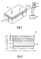
- Fig. 1 is a perspective view of the waveguide structure utilizing active phase matching; and
- Fig. 2 is a section taken along line 2-2 of Fig. 1 with the indexes of refraction (n) of the various layers depicted alongside.
- Figs. 1 and 2 illustrate an embodiment of the inventive actively phased matched
waveguide 10.
The main body of the waveguide comprises a slab of non-linearoptical material 12 such as by way of example only, potassium titanate phosphate (KTiOPO₄) known as "KTP". In asecond layer 14, Thallium (Tl) is incorporated into the KTP by diffusion or other techniques. The incorporation of thallium into KTP forms a frequency doubling waveguide since the thallium causes an increase in the index of refraction of the KTP (see the refractive index profile at Fig. 2), thus forming a non-linear optical waveguide capable of second harmonic generation. - Disposed on top of
layer 14 is buffer layer 16 of insulating material such as silicon dioxide (SiO₂) which serves to separate the waveguide oflayers first electrode layer 18 of a transparent conductor. Disposed on alayer 18 is a layer 20 of transparent semiconductor material whose index of refraction varies by the Franz-Keldysh effect in accordance with an applied electrical field. The Franz-Keldysh effect is known per se from, for example, Engineering Optics by K. Iizuka, Second Edition, Springer Verlag, p. 404-405.
Disposed above layer 20 is a second transparent conductive electrode 22, which withelectrode 18 is used to apply an electrical field to semiconductor layer 20 to vary its index of refraction. Suitable material for thetransparent electrodes 18, 22 is indium tin oxide (InSnO). Suitable semiconductor materials which have an index of refraction which varies in accordance with an applied electric field are II-VI materials such as Zinc Selenide (ZnSe) Glasses doped with II-VI particles are a possibility as well. - The structure of
device 10 is such that a change in the index of refraction of semiconductor layer 20 effects the propagation of light through the waveguide as a whole. Thus, changes to the index of refraction of layer 20 by means of the field applied tolayers 18, 22 controls the phase matching of the waveguide. Since the voltage applied betweenelectrodes 18, 22 controls the index of refraction of layer 20 which in turn controls the phase matching of theentire device 10, control over phase matching is accomplished by varying the potential applied betweenelectrodes 18 and 22. Accordingly,electrodes 18, 22 are connected to avariable voltage supply 30 the potential of which controls phase matching.Power supply 30 has a control input which in turn is connected to controlcircuitry 32 which has an input connected to adevice 34 for detecting the intensity of light of the second harmonic of the input light. Depending on the intensity of theoutput light device 34 causes controlcircuit 32 to correct the output voltage ofvoltage supply 30 thus ensuring phase matching. The actual circuitry used involtage supply 30,control 32 andlight intensity meter 34 are well known to those skilled in the art and need not be described further. - The materials used in the above-described structure are not to be construed as limiting but merely exemplary. The above-described materials namely, a KTP and thallium doped KTP waveguide utilizing a zinc selenide semiconductor layer for phase matching control is suitable for use in the frequency doubling of infrared to blue light, which as described above, is important in the field of optical storage devices. However, other materials may be used for doubling in other frequency ranges. For example, the substrate could be comprised of lithium niobiate (LiNbOo) and the semiconductor layer could be constructed from III-V materials. Furthermore,
electrodes 18 and 22 and semiconductor 20 could be replaced by a P-I-N multi-quantum well structure which would provide enhanced changes in the index of refraction. Finally, the thallium doped KTP layer could be replaced by a second ZnSe layer (inactive in frequency doubling) which eliminates the need for KTP diffusion. However, overall efficiency is likely to be reduced. - Although the present invention has been described in conjunction with preferred embodiments, it is to be understood that modifications and variations may be resorted to without departing from the scope of the invention, as those skilled in the art will readily understand. Such modifications and variations are considered to be within the purview and scope of the invention and the appended claims.
Claims (8)
- A tunable waveguide structure (10) for frequency doubling of electromagnetic radiation comprising:
a waveguide (11) having first (12) and second (14) layers of non-linear optical material, said first (12) and second (14) layers having differing indexes of refraction, characterized in that a transparent semiconductor layer (20) is disposed on one surface of said waveguide (11), said transparent semiconductor layer (20) having an index of refraction which varies by the Franz-Keldysh effect in response to an applied electrical field and that
means (18, 22) are provided for applying an electrical field to said transparent semiconductor layer (20) to vary the index of refraction of said semiconductor layer (20) to thereby control the phase matching of the waveguide (11) as a whole. - The waveguide structure (10) as claimed in Claim 1, characterized in that said means for applying a voltage comprise a transparent electrode (18, 22) disposed on each side of said semiconductor layer (20), said electrode (18, 22) being connected to a variable voltage source (30).
- The waveguide structure (10) as claimed in Claim 2, characterized in that the waveguide structure (10) further includes a buffer layer (16) disposed between said electrode (18) and said waveguide (11).
- The waveguide structure (10) as claimed in Claim 1, characterized in that said first layer (12) comprises KTP.
- The waveguide structure (10) as claimed in Claim 1, characterized in that said second layer (14) comprises thallium doped KTP.
- The waveguide structure (10) as claimed in Claim 1, characterized in that said semiconductor layer (20) comprises ZnSe.
- The waveguide structure (10) as claimed in Claim 1, characterized in that said electrodes (18, 22) comprise InSnO.
- Frequency doubling device comprising:
a semiconductor laser diode and a frequency doubling tunable waveguide structure (10), according to one of the claims 1-7.
Applications Claiming Priority (2)
| Application Number | Priority Date | Filing Date | Title |
|---|---|---|---|
| US448032 | 1989-12-08 | ||
| US07/448,032 US5046803A (en) | 1989-12-08 | 1989-12-08 | Actively phased matched frequency doubling optical waveguide |
Publications (3)
| Publication Number | Publication Date |
|---|---|
| EP0431698A2 EP0431698A2 (en) | 1991-06-12 |
| EP0431698A3 EP0431698A3 (en) | 1992-05-13 |
| EP0431698B1 true EP0431698B1 (en) | 1995-07-05 |
Family
ID=23778738
Family Applications (1)
| Application Number | Title | Priority Date | Filing Date |
|---|---|---|---|
| EP90203186A Expired - Lifetime EP0431698B1 (en) | 1989-12-08 | 1990-12-03 | Actively phase matched frequency doubling optical waveguide and frequency doubling system |
Country Status (4)
| Country | Link |
|---|---|
| US (1) | US5046803A (en) |
| EP (1) | EP0431698B1 (en) |
| JP (1) | JP3159716B2 (en) |
| DE (1) | DE69020697T2 (en) |
Families Citing this family (7)
| Publication number | Priority date | Publication date | Assignee | Title |
|---|---|---|---|---|
| US5157754A (en) * | 1990-04-25 | 1992-10-20 | E. I. Du Pont De Nemours | Wavelength conversion by quasi phase matching and the manufacture and use of optical articles therefor |
| CA2040629A1 (en) * | 1990-04-25 | 1991-10-26 | John D. Bierlein | Wavelength conversion by quasi phase matching and the manufacture and use of optical articles therefor |
| US6153318A (en) | 1996-04-30 | 2000-11-28 | Rothberg; Gerald M. | Layered material having properties that are variable by an applied electric field |
| US20030026314A1 (en) * | 1999-08-31 | 2003-02-06 | Ruey-Jen Hwu | High-power blue and green light laser generation from high-powered diode lasers |
| WO2012037445A2 (en) | 2010-09-17 | 2012-03-22 | Drexel University | Novel applications for alliform carbon |
| US9752932B2 (en) | 2010-03-10 | 2017-09-05 | Drexel University | Tunable electro-optic filter stack |
| US9178970B2 (en) | 2011-03-21 | 2015-11-03 | Apple Inc. | Electronic devices with convex displays |
Family Cites Families (3)
| Publication number | Priority date | Publication date | Assignee | Title |
|---|---|---|---|---|
| FR2193990B1 (en) * | 1972-07-25 | 1976-01-16 | Thomson Csf Fr | |
| FR2385114A1 (en) * | 1977-03-23 | 1978-10-20 | Thomson Csf | THIN-LAYER NON-LINEAR OPTICAL DEVICE AND ITS MANUFACTURING PROCESS |
| FR2471617A1 (en) * | 1979-12-14 | 1981-06-19 | Thomson Csf | NON-LINEAR COMPOSITE WAVE-GUIDED OPTICAL DEVICE AND RADIATION SOURCE USING SUCH A DEVICE |
-
1989
- 1989-12-08 US US07/448,032 patent/US5046803A/en not_active Expired - Fee Related
-
1990
- 1990-12-03 EP EP90203186A patent/EP0431698B1/en not_active Expired - Lifetime
- 1990-12-03 DE DE69020697T patent/DE69020697T2/en not_active Expired - Fee Related
- 1990-12-06 JP JP40533190A patent/JP3159716B2/en not_active Expired - Fee Related
Also Published As
| Publication number | Publication date |
|---|---|
| JP3159716B2 (en) | 2001-04-23 |
| EP0431698A2 (en) | 1991-06-12 |
| DE69020697T2 (en) | 1996-03-07 |
| DE69020697D1 (en) | 1995-08-10 |
| JPH04100024A (en) | 1992-04-02 |
| US5046803A (en) | 1991-09-10 |
| EP0431698A3 (en) | 1992-05-13 |
Similar Documents
| Publication | Publication Date | Title |
|---|---|---|
| US3898585A (en) | Leaky corrugated optical waveguide device | |
| US6914999B2 (en) | Electro-optic modulators | |
| US5155617A (en) | Electro-optic attenuated total internal reflection modulator and method | |
| US8620117B2 (en) | Optical device, optical deflection device, and optical modulation device | |
| US3877782A (en) | Electro-optical thin film device | |
| EP0355915B1 (en) | Frequency doubling device | |
| US5046803A (en) | Actively phased matched frequency doubling optical waveguide | |
| EP0434139B1 (en) | Frequency doubling optical waveguide with active phase matching | |
| EP0376710B1 (en) | A method of operating a light wavelength converter | |
| EP0027551B1 (en) | Ccd driven integrated optical modulator array | |
| US3726585A (en) | Electrically modulated radiation filters | |
| US4974923A (en) | Gap tuned optical waveguide device | |
| US3993400A (en) | Method and apparatus for forming erasable, real time, optical circuits | |
| US6204952B1 (en) | Bragg modulator | |
| Yamanouchi et al. | Optical switching device using leaky surface wave | |
| JP2899345B2 (en) | Optical device | |
| KR102320441B1 (en) | Optical intensity modulator and optical module using the same | |
| JPS6374028A (en) | light modulator | |
| JP2982366B2 (en) | Waveguide type wavelength conversion element | |
| JP2833391B2 (en) | Wavelength conversion element and multiple wavelength light source device | |
| CA1089067A (en) | Electro-optical modulator/deflector | |
| JPH0383024A (en) | Light control device | |
| JPH05224266A (en) | Plane optical device | |
| Jung | Surface plasmon resonance light modulators using electrooptic polymers. | |
| JPH05142591A (en) | Optical control circuit |
Legal Events
| Date | Code | Title | Description |
|---|---|---|---|
| PUAI | Public reference made under article 153(3) epc to a published international application that has entered the european phase |
Free format text: ORIGINAL CODE: 0009012 |
|
| AK | Designated contracting states |
Kind code of ref document: A2 Designated state(s): DE FR GB IT NL |
|
| PUAL | Search report despatched |
Free format text: ORIGINAL CODE: 0009013 |
|
| AK | Designated contracting states |
Kind code of ref document: A3 Designated state(s): DE FR GB IT NL |
|
| 17P | Request for examination filed |
Effective date: 19921111 |
|
| 17Q | First examination report despatched |
Effective date: 19940826 |
|
| GRAA | (expected) grant |
Free format text: ORIGINAL CODE: 0009210 |
|
| AK | Designated contracting states |
Kind code of ref document: B1 Designated state(s): DE FR GB IT NL |
|
| REF | Corresponds to: |
Ref document number: 69020697 Country of ref document: DE Date of ref document: 19950810 |
|
| ITF | It: translation for a ep patent filed | ||
| ET | Fr: translation filed | ||
| PLBE | No opposition filed within time limit |
Free format text: ORIGINAL CODE: 0009261 |
|
| STAA | Information on the status of an ep patent application or granted ep patent |
Free format text: STATUS: NO OPPOSITION FILED WITHIN TIME LIMIT |
|
| 26N | No opposition filed | ||
| PGFP | Annual fee paid to national office [announced via postgrant information from national office to epo] |
Ref country code: GB Payment date: 19971201 Year of fee payment: 8 |
|
| PGFP | Annual fee paid to national office [announced via postgrant information from national office to epo] |
Ref country code: FR Payment date: 19971223 Year of fee payment: 8 |
|
| PGFP | Annual fee paid to national office [announced via postgrant information from national office to epo] |
Ref country code: NL Payment date: 19971231 Year of fee payment: 8 |
|
| PGFP | Annual fee paid to national office [announced via postgrant information from national office to epo] |
Ref country code: DE Payment date: 19980223 Year of fee payment: 8 |
|
| NLT1 | Nl: modifications of names registered in virtue of documents presented to the patent office pursuant to art. 16 a, paragraph 1 |
Owner name: KONINKLIJKE PHILIPS ELECTRONICS N.V. |
|
| REG | Reference to a national code |
Ref country code: FR Ref legal event code: CD |
|
| PG25 | Lapsed in a contracting state [announced via postgrant information from national office to epo] |
Ref country code: GB Free format text: LAPSE BECAUSE OF NON-PAYMENT OF DUE FEES Effective date: 19981203 |
|
| PG25 | Lapsed in a contracting state [announced via postgrant information from national office to epo] |
Ref country code: NL Free format text: LAPSE BECAUSE OF NON-PAYMENT OF DUE FEES Effective date: 19990701 |
|
| GBPC | Gb: european patent ceased through non-payment of renewal fee |
Effective date: 19981203 |
|
| PG25 | Lapsed in a contracting state [announced via postgrant information from national office to epo] |
Ref country code: FR Free format text: LAPSE BECAUSE OF NON-PAYMENT OF DUE FEES Effective date: 19990831 |
|
| NLV4 | Nl: lapsed or anulled due to non-payment of the annual fee |
Effective date: 19990701 |
|
| REG | Reference to a national code |
Ref country code: FR Ref legal event code: ST |
|
| PG25 | Lapsed in a contracting state [announced via postgrant information from national office to epo] |
Ref country code: DE Free format text: LAPSE BECAUSE OF NON-PAYMENT OF DUE FEES Effective date: 19991001 |
|
| PG25 | Lapsed in a contracting state [announced via postgrant information from national office to epo] |
Ref country code: IT Free format text: LAPSE BECAUSE OF NON-PAYMENT OF DUE FEES;WARNING: LAPSES OF ITALIAN PATENTS WITH EFFECTIVE DATE BEFORE 2007 MAY HAVE OCCURRED AT ANY TIME BEFORE 2007. THE CORRECT EFFECTIVE DATE MAY BE DIFFERENT FROM THE ONE RECORDED. Effective date: 20051203 |