EP0425697A1 - Ultrasonic probe and method of producing the same - Google Patents
Ultrasonic probe and method of producing the same Download PDFInfo
- Publication number
- EP0425697A1 EP0425697A1 EP90907427A EP90907427A EP0425697A1 EP 0425697 A1 EP0425697 A1 EP 0425697A1 EP 90907427 A EP90907427 A EP 90907427A EP 90907427 A EP90907427 A EP 90907427A EP 0425697 A1 EP0425697 A1 EP 0425697A1
- Authority
- EP
- European Patent Office
- Prior art keywords
- ultrasonic
- wave absorber
- piezoelectric element
- junction
- ultrasonic probe
- Prior art date
- Legal status (The legal status is an assumption and is not a legal conclusion. Google has not performed a legal analysis and makes no representation as to the accuracy of the status listed.)
- Withdrawn
Links
- 239000000523 sample Substances 0.000 title claims abstract description 19
- 238000000034 method Methods 0.000 title claims description 13
- 239000006096 absorbing agent Substances 0.000 claims description 57
- 239000002245 particle Substances 0.000 claims description 7
- 238000004519 manufacturing process Methods 0.000 claims description 5
- 230000001678 irradiating effect Effects 0.000 claims description 4
- 229910000978 Pb alloy Inorganic materials 0.000 claims description 3
- 239000011888 foil Substances 0.000 claims description 3
- 229910000846 In alloy Inorganic materials 0.000 claims description 2
- 238000003825 pressing Methods 0.000 claims 1
- 239000011358 absorbing material Substances 0.000 abstract 1
- 229910052751 metal Inorganic materials 0.000 description 16
- 239000002184 metal Substances 0.000 description 16
- 239000000463 material Substances 0.000 description 9
- 238000005304 joining Methods 0.000 description 8
- 229920006332 epoxy adhesive Polymers 0.000 description 6
- 239000000843 powder Substances 0.000 description 6
- 239000003822 epoxy resin Substances 0.000 description 4
- 239000000615 nonconductor Substances 0.000 description 4
- 229920000647 polyepoxide Polymers 0.000 description 4
- 238000005245 sintering Methods 0.000 description 4
- XKRFYHLGVUSROY-UHFFFAOYSA-N Argon Chemical compound [Ar] XKRFYHLGVUSROY-UHFFFAOYSA-N 0.000 description 3
- 239000002131 composite material Substances 0.000 description 3
- 239000004020 conductor Substances 0.000 description 3
- 238000010438 heat treatment Methods 0.000 description 3
- 229910001385 heavy metal Inorganic materials 0.000 description 3
- 239000004033 plastic Substances 0.000 description 3
- 230000001681 protective effect Effects 0.000 description 3
- XEEYBQQBJWHFJM-UHFFFAOYSA-N Iron Chemical compound [Fe] XEEYBQQBJWHFJM-UHFFFAOYSA-N 0.000 description 2
- 241001676573 Minium Species 0.000 description 2
- PXHVJJICTQNCMI-UHFFFAOYSA-N Nickel Chemical compound [Ni] PXHVJJICTQNCMI-UHFFFAOYSA-N 0.000 description 2
- 229910020220 Pb—Sn Inorganic materials 0.000 description 2
- 229910001128 Sn alloy Inorganic materials 0.000 description 2
- 229910045601 alloy Inorganic materials 0.000 description 2
- 239000000956 alloy Substances 0.000 description 2
- 229910052786 argon Inorganic materials 0.000 description 2
- 238000005219 brazing Methods 0.000 description 2
- 239000000356 contaminant Substances 0.000 description 2
- 230000000694 effects Effects 0.000 description 2
- 239000000945 filler Substances 0.000 description 2
- 235000011194 food seasoning agent Nutrition 0.000 description 2
- 238000010884 ion-beam technique Methods 0.000 description 2
- 239000007769 metal material Substances 0.000 description 2
- 150000002739 metals Chemical class 0.000 description 2
- 239000000203 mixture Substances 0.000 description 2
- 238000009659 non-destructive testing Methods 0.000 description 2
- 230000000644 propagated effect Effects 0.000 description 2
- RYGMFSIKBFXOCR-UHFFFAOYSA-N Copper Chemical compound [Cu] RYGMFSIKBFXOCR-UHFFFAOYSA-N 0.000 description 1
- 229910000640 Fe alloy Inorganic materials 0.000 description 1
- HCHKCACWOHOZIP-UHFFFAOYSA-N Zinc Chemical compound [Zn] HCHKCACWOHOZIP-UHFFFAOYSA-N 0.000 description 1
- 239000000853 adhesive Substances 0.000 description 1
- 230000001070 adhesive effect Effects 0.000 description 1
- PNEYBMLMFCGWSK-UHFFFAOYSA-N aluminium oxide Inorganic materials [O-2].[O-2].[O-2].[Al+3].[Al+3] PNEYBMLMFCGWSK-UHFFFAOYSA-N 0.000 description 1
- 230000015556 catabolic process Effects 0.000 description 1
- 239000000919 ceramic Substances 0.000 description 1
- 229910010293 ceramic material Inorganic materials 0.000 description 1
- 238000001816 cooling Methods 0.000 description 1
- 229910052802 copper Inorganic materials 0.000 description 1
- 239000010949 copper Substances 0.000 description 1
- 230000007547 defect Effects 0.000 description 1
- 238000006731 degradation reaction Methods 0.000 description 1
- 230000001419 dependent effect Effects 0.000 description 1
- 238000001514 detection method Methods 0.000 description 1
- 230000001627 detrimental effect Effects 0.000 description 1
- 230000001747 exhibiting effect Effects 0.000 description 1
- 239000007789 gas Substances 0.000 description 1
- PCHJSUWPFVWCPO-UHFFFAOYSA-N gold Chemical compound [Au] PCHJSUWPFVWCPO-UHFFFAOYSA-N 0.000 description 1
- 229910052737 gold Inorganic materials 0.000 description 1
- 239000010931 gold Substances 0.000 description 1
- 229910052738 indium Inorganic materials 0.000 description 1
- APFVFJFRJDLVQX-UHFFFAOYSA-N indium atom Chemical compound [In] APFVFJFRJDLVQX-UHFFFAOYSA-N 0.000 description 1
- 238000002347 injection Methods 0.000 description 1
- 239000007924 injection Substances 0.000 description 1
- 229910052742 iron Inorganic materials 0.000 description 1
- WABPQHHGFIMREM-UHFFFAOYSA-N lead(0) Chemical group [Pb] WABPQHHGFIMREM-UHFFFAOYSA-N 0.000 description 1
- 238000002844 melting Methods 0.000 description 1
- 230000008018 melting Effects 0.000 description 1
- 238000002156 mixing Methods 0.000 description 1
- 229910052759 nickel Inorganic materials 0.000 description 1
- 235000014593 oils and fats Nutrition 0.000 description 1
- 230000003647 oxidation Effects 0.000 description 1
- 238000007254 oxidation reaction Methods 0.000 description 1
- 238000007747 plating Methods 0.000 description 1
- 230000001737 promoting effect Effects 0.000 description 1
- 230000001902 propagating effect Effects 0.000 description 1
- 238000002310 reflectometry Methods 0.000 description 1
- 229920005989 resin Polymers 0.000 description 1
- 239000011347 resin Substances 0.000 description 1
- 229910052709 silver Inorganic materials 0.000 description 1
- 239000004332 silver Substances 0.000 description 1
- 239000007787 solid Substances 0.000 description 1
- 238000004544 sputter deposition Methods 0.000 description 1
- 238000006467 substitution reaction Methods 0.000 description 1
- WFKWXMTUELFFGS-UHFFFAOYSA-N tungsten Chemical compound [W] WFKWXMTUELFFGS-UHFFFAOYSA-N 0.000 description 1
- 229910052721 tungsten Inorganic materials 0.000 description 1
- 239000010937 tungsten Substances 0.000 description 1
- 229910052725 zinc Inorganic materials 0.000 description 1
- 239000011701 zinc Substances 0.000 description 1
- 229910052726 zirconium Inorganic materials 0.000 description 1
Images

Classifications
-
- B—PERFORMING OPERATIONS; TRANSPORTING
- B06—GENERATING OR TRANSMITTING MECHANICAL VIBRATIONS IN GENERAL
- B06B—METHODS OR APPARATUS FOR GENERATING OR TRANSMITTING MECHANICAL VIBRATIONS OF INFRASONIC, SONIC, OR ULTRASONIC FREQUENCY, e.g. FOR PERFORMING MECHANICAL WORK IN GENERAL
- B06B1/00—Methods or apparatus for generating mechanical vibrations of infrasonic, sonic, or ultrasonic frequency
- B06B1/02—Methods or apparatus for generating mechanical vibrations of infrasonic, sonic, or ultrasonic frequency making use of electrical energy
- B06B1/06—Methods or apparatus for generating mechanical vibrations of infrasonic, sonic, or ultrasonic frequency making use of electrical energy operating with piezoelectric effect or with electrostriction
- B06B1/0644—Methods or apparatus for generating mechanical vibrations of infrasonic, sonic, or ultrasonic frequency making use of electrical energy operating with piezoelectric effect or with electrostriction using a single piezoelectric element
- B06B1/0662—Methods or apparatus for generating mechanical vibrations of infrasonic, sonic, or ultrasonic frequency making use of electrical energy operating with piezoelectric effect or with electrostriction using a single piezoelectric element with an electrode on the sensitive surface
- B06B1/0681—Methods or apparatus for generating mechanical vibrations of infrasonic, sonic, or ultrasonic frequency making use of electrical energy operating with piezoelectric effect or with electrostriction using a single piezoelectric element with an electrode on the sensitive surface and a damping structure
-
- H—ELECTRICITY
- H04—ELECTRIC COMMUNICATION TECHNIQUE
- H04R—LOUDSPEAKERS, MICROPHONES, GRAMOPHONE PICK-UPS OR LIKE ACOUSTIC ELECTROMECHANICAL TRANSDUCERS; DEAF-AID SETS; PUBLIC ADDRESS SYSTEMS
- H04R17/00—Piezoelectric transducers; Electrostrictive transducers
-
- G—PHYSICS
- G10—MUSICAL INSTRUMENTS; ACOUSTICS
- G10K—SOUND-PRODUCING DEVICES; METHODS OR DEVICES FOR PROTECTING AGAINST, OR FOR DAMPING, NOISE OR OTHER ACOUSTIC WAVES IN GENERAL; ACOUSTICS NOT OTHERWISE PROVIDED FOR
- G10K11/00—Methods or devices for transmitting, conducting or directing sound in general; Methods or devices for protecting against, or for damping, noise or other acoustic waves in general
- G10K11/02—Mechanical acoustic impedances; Impedance matching, e.g. by horns; Acoustic resonators
Definitions
- This invention relates to the structure of a junction between a piezoelectric element and an ultrasonic-wave absorber in an ultrasonic probe and relates also to a method for manufacturing such an ultrasonic probe.
- An ultrasonic-wave absorber and a piezoelectric element have hitherto been joined together by a method in which they are bonded by the use of an epoxy adhesive and also by a method in which a composite material prepared by mixing a heavy-metal filler with an epoxy resin is used as an ultrasonic-wave absorber, and a piezoelectric element is cast in the step of curing the ultrasonic-wave absrober.
- the related art includes the disclosures of JP-A-60-58550 and JP-A-60-128358.
- the priorart has had such another problem that the ultrasonic waves do not sufficiently propagate from the piezoelectric element toward the ultrasonic-wave absorber, and detrimental reverberation of the ultrasonic waves cannot be efficiently absorbed by the ultrasonic-wave absorber.
- the ultrasonic-wave absorber When a material having an acoustic impedance substantially equivalent to that of the piezoelectric element is employed as the ultrasonic-wave absorber, the ultrasonic waves generated from the piezoelectric element and propagating toward the ultrasonic-wave absorber are efficiently absorbed by the ultrasonic-wave absorber, so that the unnecessary reverberation would not occur.
- the piezoelectric element and the ultrasonic-wave absorber must be joined together without the use of the adhesive. This purpose will be attained by employing a metal material to form the ultrasonic-wave absorber and utilizing the joinability of the metal itself so as to join the ultrasonic-wave absorber to the piezoelectric element.
- a method is commonly employed in which the metal is joined by heating it to a level higher than or close to its melting point.
- a joining method is employed so as to join the absorber to the piezoelectric element, the surface flatness of the piezoelectric element is lost due to a thermal strain attributable to a change in the temperature of the absorber, thereby giving rise to a degraded performance of the ultrasonic probe.
- this thermal strain causes a seasoning deformation, with the result that the performance of the probe becomes unstable. Further, when this thermal strain is excessively large, breakage of the piezoelectric element tends to results, and the practical use of the ultrasonic probe will become utterly impossible.
- the prior art has had the necessity for forming electrodes on the piezoelectric element, because the ultrasonic-wave absorber formed of an electrical insulator is used, or the ultrasonic-wave absrober formed of an electrical conductor is joined to the piezoelectric element by the use of the epoxy adhesive which is an electrical insulator. Also, the prior art has had such another problem that the strength of the joints between the electrodes and the piezoelectric element is weak, and the electrodes tend to be stripped off from the piezoelectric element during use.
- the present invention which attains the above object, for the purpose of joining the piezoelectric element to the ultrasonic-wave absorber formed of a metal or formed by sintering metal powders, their junction surfaces are irradiated with a particle beam in a vacuum, and they are then pressed against each other at a temperature lower than the Curie point of the oscillator.
- a foil or film of an In alloy or an Fe alloy is inserted as an insert member, and the piezoelectric element and the ultrasonic-wave absorber are then pressed against each other while irradiating their junction surfaces with the particle beam in the vacuum.
- junction surface of the piezoelectric element and that of the ultrasonic-wave absorber which is formed of the metal or formed by sintering the metal powders, with the particle beam in the vacuum, oils and fats, moisture, oxide films, etc. attaching to their junction surfaces are removed. As a result, hands of bond are exposed on the junction surfaces to provide highly active surfaces forming a firm junction, so that the piezoelectric element and the ultrasonic-wave absorber are firmly joined together when brought into intimate contact with each other under application of a pressure.
- the energy injection is limited to the irradiated surfaces only. Therefore, when compared to the method of joining by heating the ultrasonic-wave absorber, the quantity of energy injected into the entire ultrasonic-wave absorber is very small. As a result, the thermal strain would hardly occur on the ultrasonic-wave absorber, and, therefore, the piezoelectric element maintains its surface flatness.
- the ultrasonic-wave absorber When the ultrasonic-wave absorber is such that it cannot be sufficiently joined to the piezoelectric element in spite of the irradiation with the particle beam, a firm junction can be attained when an insert member showing a good joinability to both the piezoelectric element and the ultrasonic-wave absorber is inserted into the junction surfaces.
- the insert member When the insert member is used, the insert member is subjected to plastic deformation during application of the joining pressure, thereby improving the degree of intimate contact at the junction interface, so that a more firm and uniform junction can be provided.
- both the ultrasonic-wave absorber and the insert member are electrical conductors, they can be used as electrodes.
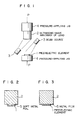
- Fig. 1 is a front elevational view showing a method for establishing a metal-to-metal junction between a piezoelectric element and an ultrasonic-wave absorber.
- Figs. 2 and 3 are longitudinal sectional views each showing the structure of the junction between the piezoelectric element and the ultrasonic-wave absorber formed of lead.
- Fig. 4 is a longitudinal sectional view of an embodiment of the ultrasonic probe of the present invention.
- 1 designates a piezoelectric element
- 2 designates an ultrasonic-wave absorber formed of lead
- 3 designates each of beam sources emitting an atom beam
- 4 designates each of pressure applying jigs.
- the piezoelectric element 1 and the ultrasonic-wave absorber 2 are mounted on the pressure applying jigs 4, and the atmosphere is evacuated to a vacuum of 2x10 ⁇ 7 Torr. Then, argon gas is introduced into the beam sources 3 to set the pressure of the atmosphere at 4x10 ⁇ 4 Torr, and argon atom beams emitted from the beam sources 3 are directed toward and onto the junction surfaces of both the piezoelectric element and the ultrasonic-wave absorber 2 so as to remove contaminants and surface films. Because the junction surfaces from which the contaminants and the surface films are removed have a very high degree of joinability, a metal-to-metal junction is easily formed when the junction surfaces are brought into intimate contact with each other by application of a pressure P at the room temperature.
- the piezoelectric element 1 and the ultrasonic-wave absorber 2 are directly joined.
- a foil 5 of a soft metal which is liable to plastic deformation such as, an In-Sn alloy, an In-Pb alloy or a Pb-Sn alloy may be used as an insert member.
- a foil 5 of a soft metal which is liable to plastic deformation such as, an In-Sn alloy, an In-Pb alloy or a Pb-Sn alloy may be used as an insert member.
- a film 6 of a soft metal such as an In-Sn alloy, an In-Pb alloy or a Pb-Sn alloy or of an oxidation resistive metal such as gold or silver may be formed on the junction surface of the piezoelectric element 1 or the ultrasonic-wave absorber of lead 2 by means such as sputtering, plating or brazing, so as to realize a firm junction without hardly abstructing propagation of ultrasonic waves.
- any one of metals such as tungsten, zinc, iron, nickel, copper and indium having a large acoustic impedance can be used as the material of the ultrasonic-wave absorber 2, besides lead.
- a material having an acoustic impedance close to that of the piezoelectric element 1 and acting to greatly attenuate ultrasonic waves is most preferable.
- lead is most suitable for the purpose.
- the desired effect can be similarly exhibited even when any one of sintered bodies obtained by sintering powders or powder mixtures of metals having an acoustic impedance larger than that of the piezoelectric element 1 (Column 2 in Table 1) is used.
- an atom beam (neutron rays) is used as the particle beam. This is because the atom beam does not cause charge-up of an object to be irradiated and is therefore suitable for irradiation of an electrical insulator such as a ceramic oscillator.
- An ion beam can be also used as the particle beam. However, when the ion beam is used for irradiating an electrical insulator, it is necessary to simultaneously direct an electron shower so as to prevent charge-up.
- Fig. 4 designates the piezoelectric element
- 2 designates the ultrasonic-wave absorber formed of lead
- 7 designates a protective plate formed of alumina
- 8 designates a lead wire connected to the electrode
- 9 designates a filler
- 10 designates a protective case
- 11 designates a terminal.
- the ultrasonic-wave absorber 2 formed of lead is an electrical conductor and can be used as an electrode for the piezoelectric element 1.
- Ultrasonic pulses are generated when a pulse voltage from a pulse voltage generator (not shown) is applied to the piezoelectric element 1 through the terminal 11.
- the generated ultrasonic waves are injected through the protective plate 7 toward and into an object to be tested (not shown) for the purpose of ultrasonic nondestructive testing.
- Reverberation of the ultrasonic waves which degrades both the accuracy of the ultrasonic nondestructive testing and the capability of fault or defect detection, is absorbed by the ultrasonic-wave absorber of lead 2 joined to the piezoelectric element 1.
- Table 2 shows representative values of acoustic impedances of various materials.
- a composite material which consists of a heavy metal and a resin and whose typical example is a composite material consisting of minium and an epoxy resin has hitherto been widely employed as the material of the ultrasonic-wave absorber.
- the acoustic impedance is 0.5x10⁶ g cm/s as shown in Table 2 and is for smaller than 2.3x10⁶ g cm/s which is the typical value of the acoustic impedance of the piezoelectric element (the ceramic material having the composition of (Pb(Zr, Ti)O3-PbMo)).
- the insert member is a solid, its thickness can be easily controlled. Therefore, when the thickness of the insert member is selected to be equal to 1/4 ⁇ ( ⁇ : the wavelength of ultrasonic waves), an acoustic matching layer can be formed, so that the reverberation of the ultrasonic waves can be efficiently propagated toward the ultrasonic-wave absorber.
- ⁇ the wavelength of ultrasonic waves
- An ultrasonic probe in which the acoustic wave reverberation time does not change over a long period of time can be provided, because a metal material having a property free from any secular variation can be used to form its ultrasonic-wave absorber. Also, because a metal having a large acoustic impedance can be used as the material of the ultrasonic-wave absorber, reflection of the ultrasonic wave at the interface between the piezoelectric element and the ultrasonic wave absorber can be minimized.
- the oscillator and the ultrasonic-wave absorber are joined together at the room temperature in the illustrated embodiment, no residual thermal strain attributable to joining occurs.
- the coefficient of linear expansion of the ultrasonic-wave absorber is not generally equal to that of the oscillator. Therefore, when they are joined at a high temperature, problems including a variation of the piezoelectric characteristic of the oscillator due to a residual thermal strain and degradation of the surface flatness of the oscillator after cooling arise, resulting sometimes in breakage of the oscillator, strip-off at the junction part, etc. These problems do not arise in the illustrated embodiment in which joining is made at the room temperature.
- Electrodes for the piezoelectric element have hitherto been formed by brazing.
- the ultrasonic-wave absorber formed of a metal can be used as one of the electrodes.
Abstract
Description
- This invention relates to the structure of a junction between a piezoelectric element and an ultrasonic-wave absorber in an ultrasonic probe and relates also to a method for manufacturing such an ultrasonic probe.
- An ultrasonic-wave absorber and a piezoelectric element have hitherto been joined together by a method in which they are bonded by the use of an epoxy adhesive and also by a method in which a composite material prepared by mixing a heavy-metal filler with an epoxy resin is used as an ultrasonic-wave absorber, and a piezoelectric element is cast in the step of curing the ultrasonic-wave absrober.
- The related art includes the disclosures of JP-A-60-58550 and JP-A-60-128358.
- In the prior art described above, a seasoning deformation of the epoxy resin mixed with the heavy metal and that of the epoxy adhesive are not taken into consideration, and the prior art has thus had the problem that the acoustic characteristics of the ultrasonic probe are degraded with time. Also, because of a very large difference between the acoustic impedance of the epoxy adhesive and that of the piezoelectric element or that of the ultrasonic-wave absorber, the epoxy adhesive forms an acoustic boundary layer when the piezoelectric element and the ultrasonic-wave absorber are joined together by the use of the epoxy adhesive, and this results in reflection of the ultrasonic waves. Therefore, the priorart has had such another problem that the ultrasonic waves do not sufficiently propagate from the piezoelectric element toward the ultrasonic-wave absorber, and detrimental reverberation of the ultrasonic waves cannot be efficiently absorbed by the ultrasonic-wave absorber.
- When a material having an acoustic impedance substantially equivalent to that of the piezoelectric element is employed as the ultrasonic-wave absorber, the ultrasonic waves generated from the piezoelectric element and propagating toward the ultrasonic-wave absorber are efficiently absorbed by the ultrasonic-wave absorber, so that the unnecessary reverberation would not occur. For that purpose, the piezoelectric element and the ultrasonic-wave absorber must be joined together without the use of the adhesive. This purpose will be attained by employing a metal material to form the ultrasonic-wave absorber and utilizing the joinability of the metal itself so as to join the ultrasonic-wave absorber to the piezoelectric element. As such a joining method, a method is commonly employed in which the metal is joined by heating it to a level higher than or close to its melting point. However, when such a joining method is employed so as to join the absorber to the piezoelectric element, the surface flatness of the piezoelectric element is lost due to a thermal strain attributable to a change in the temperature of the absorber, thereby giving rise to a degraded performance of the ultrasonic probe. Also, this thermal strain causes a seasoning deformation, with the result that the performance of the probe becomes unstable. Further, when this thermal strain is excessively large, breakage of the piezoelectric element tends to results, and the practical use of the ultrasonic probe will become utterly impossible.
- The prior art has had the necessity for forming electrodes on the piezoelectric element, because the ultrasonic-wave absorber formed of an electrical insulator is used, or the ultrasonic-wave absrober formed of an electrical conductor is joined to the piezoelectric element by the use of the epoxy adhesive which is an electrical insulator. Also, the prior art has had such another problem that the strength of the joints between the electrodes and the piezoelectric element is weak, and the electrodes tend to be stripped off from the piezoelectric element during use.
- It is an object of the present invention to provide the structure of an ultrasonic probe in which its piezoelectric element and its ultrasonic-wave absorber are joined together with a high strength, in which reverberation of ultrasonic waves can be efficiently absorbed, and in which the ultrasonic-wave absorber can be used as an electrode and to provide also a method for manufacturing such an ultrasonic probe.
- According to the present invention which attains the above object, for the purpose of joining the piezoelectric element to the ultrasonic-wave absorber formed of a metal or formed by sintering metal powders, their junction surfaces are irradiated with a particle beam in a vacuum, and they are then pressed against each other at a temperature lower than the Curie point of the oscillator.
- Further, at the time of joining, a foil or film of an In alloy or an Fe alloy is inserted as an insert member, and the piezoelectric element and the ultrasonic-wave absorber are then pressed against each other while irradiating their junction surfaces with the particle beam in the vacuum.
- By irradiating the junction surface of the piezoelectric element and that of the ultrasonic-wave absorber, which is formed of the metal or formed by sintering the metal powders, with the particle beam in the vacuum, oils and fats, moisture, oxide films, etc. attaching to their junction surfaces are removed. As a result, hands of bond are exposed on the junction surfaces to provide highly active surfaces forming a firm junction, so that the piezoelectric element and the ultrasonic-wave absorber are firmly joined together when brought into intimate contact with each other under application of a pressure.
- Although high energy is injected into the irradiated surfaces according to this method, the energy injection is limited to the irradiated surfaces only. Therefore, when compared to the method of joining by heating the ultrasonic-wave absorber, the quantity of energy injected into the entire ultrasonic-wave absorber is very small. As a result, the thermal strain would hardly occur on the ultrasonic-wave absorber, and, therefore, the piezoelectric element maintains its surface flatness.
- When the ultrasonic-wave absorber is such that it cannot be sufficiently joined to the piezoelectric element in spite of the irradiation with the particle beam, a firm junction can be attained when an insert member showing a good joinability to both the piezoelectric element and the ultrasonic-wave absorber is inserted into the junction surfaces. When the insert member is used, the insert member is subjected to plastic deformation during application of the joining pressure, thereby improving the degree of intimate contact at the junction interface, so that a more firm and uniform junction can be provided.
- Further, because both the ultrasonic-wave absorber and the insert member are electrical conductors, they can be used as electrodes.
- Fig. 1 is a front elevational view showing a method for establishing a metal-to-metal junction between a piezoelectric element and an ultrasonic-wave absorber.
- Figs. 2 and 3 are longitudinal sectional views each showing the structure of the junction between the piezoelectric element and the ultrasonic-wave absorber formed of lead.
- Fig. 4 is a longitudinal sectional view of an embodiment of the ultrasonic probe of the present invention.
- An embodiment of the present invention will now be described with reference to Fig. 1.
- 1 designates a piezoelectric element, 2 designates an ultrasonic-wave absorber formed of lead, 3 designates each of beam sources emitting an atom beam, and 4 designates each of pressure applying jigs.
- First, the piezoelectric element 1 and the ultrasonic-
wave absorber 2 are mounted on thepressure applying jigs 4, and the atmosphere is evacuated to a vacuum of 2x10⁻⁷ Torr. Then, argon gas is introduced into thebeam sources 3 to set the pressure of the atmosphere at 4x10⁻⁴ Torr, and argon atom beams emitted from thebeam sources 3 are directed toward and onto the junction surfaces of both the piezoelectric element and the ultrasonic-wave absorber 2 so as to remove contaminants and surface films. Because the junction surfaces from which the contaminants and the surface films are removed have a very high degree of joinability, a metal-to-metal junction is easily formed when the junction surfaces are brought into intimate contact with each other by application of a pressure P at the room temperature. - In the illustrated embodiment, the piezoelectric element 1 and the ultrasonic-
wave absorber 2 are directly joined. However, as shown in Fig. 2, afoil 5 of a soft metal which is liable to plastic deformation, such as, an In-Sn alloy, an In-Pb alloy or a Pb-Sn alloy may be used as an insert member. Also, as shown in Fig. 3, afilm 6 of a soft metal such as an In-Sn alloy, an In-Pb alloy or a Pb-Sn alloy or of an oxidation resistive metal such as gold or silver may be formed on the junction surface of the piezoelectric element 1 or the ultrasonic-wave absorber oflead 2 by means such as sputtering, plating or brazing, so as to realize a firm junction without hardly abstructing propagation of ultrasonic waves. - Further, as shown in Table 1, any one of metals such as tungsten, zinc, iron, nickel, copper and indium having a large acoustic impedance (Column 1 in Table 1) can be used as the material of the ultrasonic-
wave absorber 2, besides lead. Among those materials, a material having an acoustic impedance close to that of the piezoelectric element 1 and acting to greatly attenuate ultrasonic waves is most preferable. From this viewpoint, lead is most suitable for the purpose. However, the desired effect can be similarly exhibited even when any one of sintered bodies obtained by sintering powders or powder mixtures of metals having an acoustic impedance larger than that of the piezoelectric element 1 (Column 2 in Table 1) is used. - In the illustrated embodiment, an atom beam (neutron rays) is used as the particle beam. This is because the atom beam does not cause charge-up of an object to be irradiated and is therefore suitable for irradiation of an electrical insulator such as a ceramic oscillator. An ion beam can be also used as the particle beam. However, when the ion beam is used for irradiating an electrical insulator, it is necessary to simultaneously direct an electron shower so as to prevent charge-up.

- The structure and operation of the ultrasonic probe manufactured according to the present invention will now be described with reference to Fig. 4. 1 designates the piezoelectric element, 2 designates the ultrasonic-wave absorber formed of lead, 7 designates a protective plate formed of alumina, 8 designates a lead wire connected to the electrode, 9 designates a filler, 10 designates a protective case, and 11 designates a terminal. The ultrasonic-
wave absorber 2 formed of lead is an electrical conductor and can be used as an electrode for the piezoelectric element 1. - The operation will now be described. Ultrasonic pulses are generated when a pulse voltage from a pulse voltage generator (not shown) is applied to the piezoelectric element 1 through the terminal 11. The generated ultrasonic waves are injected through the
protective plate 7 toward and into an object to be tested (not shown) for the purpose of ultrasonic nondestructive testing. Reverberation of the ultrasonic waves, which degrades both the accuracy of the ultrasonic nondestructive testing and the capability of fault or defect detection, is absorbed by the ultrasonic-wave absorber oflead 2 joined to the piezoelectric element 1. - Table 2 shows representative values of acoustic impedances of various materials. A composite material which consists of a heavy metal and a resin and whose typical example is a composite material consisting of minium and an epoxy resin has hitherto been widely employed as the material of the ultrasonic-wave absorber. However, in this case, the acoustic impedance is 0.5x10⁶ g cm/s as shown in Table 2 and is for smaller than 2.3x10⁶ g cm/s which is the typical value of the acoustic impedance of the piezoelectric element (the ceramic material having the composition of (Pb(Zr, Ti)O₃-PbMo)).
- When the piezoelectric element and the ultrasonic-wave absorber have acoustic impedance ZC and ZD respectively, the acoustic reflectivity r at their junction interface is given by the following equation:

- When, for example, the piezoelectric element is joined to the epoxy resin containing the minium, substitution of the value of the acoustic impedance shown in Table 2 into the equation (1) provides the result of r=61%. Thus, it is proved that more thant he half of the acoustic waves are reflected at the acoustic waves do not efficiently propagate toward the ultrasonic-wave absorber.

- On the other hand, when lead is used as the material of the ultrasonic-wave absorber, r=4% is derived from the equation (1) in view of the acoustic impedance value shown in Table 2. Thus, reflection of the ultrasonic waves at the junction interface is minimized, so that the ultrasonic waves can be efficiently propagated toward the ultrasonic-wave absorber. The illustrated embodiment exhibits the effect that unnecessary reverberation of ultrasonic waves can be extinguished within a very short period of time.
- It is known that the less the reverberation of ultrasonic waves, the performance of the ultrasonic probe is higher. When the oscillator, the insert member and the ultrasonic-wave absorber have acoustic impedances ZE, Zi and ZD respectively, the order of the performance of the ultrasonic probe dependent on the relative amounts of the acoustic impedances is as follows:
- 1. ZE = Zi = ZD
- 2. ZE > Zi = ZD
- 3. ZE > Zi > ZD
- 4. ZE > Zi < ZD
- In the case of the sintered body obtained by sintering metal powders, the relation Zi=ZD or Zi>ZD can be easily provided, because the acoustic impedance can be controlled over a wide range by suitably selecting the ratio of the mixed materials. Therefore, when the metal-powder sintered body is used as the ultrasonic-wave absorber, the probe exhibiting high performance can be easily manufactured.
- Further, because the insert member is a solid, its thickness can be easily controlled. Therefore, when the thickness of the insert member is selected to be equal to 1/4 λ (λ: the wavelength of ultrasonic waves), an acoustic matching layer can be formed, so that the reverberation of the ultrasonic waves can be efficiently propagated toward the ultrasonic-wave absorber.
- An ultrasonic probe in which the acoustic wave reverberation time does not change over a long period of time can be provided, because a metal material having a property free from any secular variation can be used to form its ultrasonic-wave absorber. Also, because a metal having a large acoustic impedance can be used as the material of the ultrasonic-wave absorber, reflection of the ultrasonic wave at the interface between the piezoelectric element and the ultrasonic wave absorber can be minimized.
- Further, because the oscillator and the ultrasonic-wave absorber are joined together at the room temperature in the illustrated embodiment, no residual thermal strain attributable to joining occurs. The coefficient of linear expansion of the ultrasonic-wave absorber is not generally equal to that of the oscillator. Therefore, when they are joined at a high temperature, problems including a variation of the piezoelectric characteristic of the oscillator due to a residual thermal strain and degradation of the surface flatness of the oscillator after cooling arise, resulting sometimes in breakage of the oscillator, strip-off at the junction part, etc. These problems do not arise in the illustrated embodiment in which joining is made at the room temperature. However, when temperature range where a variation of the piezoelectric characteristic or a variation of the surface flatness of the oscillator falls in an allowable range, the yield strength of the ultrasonic-wave absorber or the insert member is lowered to increase of plastic deformability. Thus, heating is effective for promoting the intimate contact at the junction, thereby improving both the junction strength and the reliability.
- Electrodes for the piezoelectric element have hitherto been formed by brazing. According to the present invention, the ultrasonic-wave absorber formed of a metal can be used as one of the electrodes. Thus, it is merely necessary to form the other electrode on one surface only of the piezoelectric element, thereby simplifying the steps of manufacturing the piezoelectric element.
Claims (3)
- A method for manufacturing an ultrasonic probe characterized by irradiating junction surfaces of a piezoelectric element and an ultrasonic-wave absorber with a particle beam in a vacuum and then pressing the two junction surfaces against each other by application of a pressure.
- An ultrasonic probe characterized in that an ultrasonic-wave absorber joined to a piezoelectric element is used as an electrode.
- A method for manufacturing an ultrasonic probe as claimed in Claim 2, characterized in that a foil of an In alloy or a Pb alloy is inserted between the piezoelectric element and the ultrasonic-wave absorber.
Applications Claiming Priority (2)
| Application Number | Priority Date | Filing Date | Title |
|---|---|---|---|
| JP11867689 | 1989-05-15 | ||
| JP118676/89 | 1989-05-15 |
Publications (2)
| Publication Number | Publication Date |
|---|---|
| EP0425697A1 true EP0425697A1 (en) | 1991-05-08 |
| EP0425697A4 EP0425697A4 (en) | 1992-12-02 |
Family
ID=14742449
Family Applications (1)
| Application Number | Title | Priority Date | Filing Date |
|---|---|---|---|
| EP19900907427 Withdrawn EP0425697A4 (en) | 1989-05-15 | 1990-05-14 | Ultrasonic probe and method of producing the same |
Country Status (3)
| Country | Link |
|---|---|
| EP (1) | EP0425697A4 (en) |
| KR (1) | KR920702178A (en) |
| WO (1) | WO1990014738A1 (en) |
Cited By (3)
| Publication number | Priority date | Publication date | Assignee | Title |
|---|---|---|---|---|
| EP0634227A2 (en) * | 1993-07-15 | 1995-01-18 | General Electric Company | Broadband ultrasonic transducers and related method of manufacture |
| US6084334A (en) * | 1997-10-29 | 2000-07-04 | Canon Kabushiki Kaisha | Driving apparatus for driving plurality of vibration type motors |
| WO2023235531A1 (en) * | 2022-06-03 | 2023-12-07 | Trophy Sas | Compact ultrasound transducers for intraoral uses |
Families Citing this family (1)
| Publication number | Priority date | Publication date | Assignee | Title |
|---|---|---|---|---|
| KR19990078789A (en) * | 1999-08-07 | 1999-11-05 | 한진호 | Medical ultrasonic probe by using plasma etching |
Citations (5)
| Publication number | Priority date | Publication date | Assignee | Title |
|---|---|---|---|---|
| FR2097451A5 (en) * | 1970-07-07 | 1972-03-03 | Commissariat Energie Atomique | |
| FR2251149A1 (en) * | 1973-11-14 | 1975-06-06 | Commissariat Energie Atomique | Piezoelectric transducer damping device - has shaped piece of high energy dissipating rate material to attenuate pulses |
| JPS5931278A (en) * | 1982-08-11 | 1984-02-20 | 株式会社日立製作所 | Man conveyor |
| US4434384A (en) * | 1980-12-08 | 1984-02-28 | Raytheon Company | Ultrasonic transducer and its method of manufacture |
| JPS60160300A (en) * | 1984-01-30 | 1985-08-21 | Nippon Dempa Kogyo Co Ltd | Manufacture of array-type ultrasonic wave probe |
Family Cites Families (3)
| Publication number | Priority date | Publication date | Assignee | Title |
|---|---|---|---|---|
| JPS5575646A (en) * | 1978-12-04 | 1980-06-07 | Mitsubishi Electric Corp | Probe for electroacoustic conversion |
| JPS5912079B2 (en) * | 1979-03-13 | 1984-03-21 | 東レ株式会社 | ultrasonic transducer |
| JPS63255657A (en) * | 1987-04-14 | 1988-10-21 | Ishikawajima Harima Heavy Ind Co Ltd | Manufacture of damper material for probe |
-
1990
- 1990-05-14 KR KR1019910700055A patent/KR920702178A/en not_active Application Discontinuation
- 1990-05-14 WO PCT/JP1990/000605 patent/WO1990014738A1/en not_active Application Discontinuation
- 1990-05-14 EP EP19900907427 patent/EP0425697A4/en not_active Withdrawn
Patent Citations (5)
| Publication number | Priority date | Publication date | Assignee | Title |
|---|---|---|---|---|
| FR2097451A5 (en) * | 1970-07-07 | 1972-03-03 | Commissariat Energie Atomique | |
| FR2251149A1 (en) * | 1973-11-14 | 1975-06-06 | Commissariat Energie Atomique | Piezoelectric transducer damping device - has shaped piece of high energy dissipating rate material to attenuate pulses |
| US4434384A (en) * | 1980-12-08 | 1984-02-28 | Raytheon Company | Ultrasonic transducer and its method of manufacture |
| JPS5931278A (en) * | 1982-08-11 | 1984-02-20 | 株式会社日立製作所 | Man conveyor |
| JPS60160300A (en) * | 1984-01-30 | 1985-08-21 | Nippon Dempa Kogyo Co Ltd | Manufacture of array-type ultrasonic wave probe |
Non-Patent Citations (3)
| Title |
|---|
| DATABASE WPIL Section Ch, Week 8437, Derwent Publications Ltd., London, GB; Class L03, AN 84-229199 & JP-A-59 031 278 ((VICO) VICTOR COMPANY OF JAPAN) 1 August 1984 * |
| PATENT ABSTRACTS OF JAPAN vol. 9, no. 328 (E-369)24 December 1985 & JP-A-60 160 300 ( NIHON DENPA KOGYO KK ) 21 August 1985 * |
| See also references of WO9014738A1 * |
Cited By (4)
| Publication number | Priority date | Publication date | Assignee | Title |
|---|---|---|---|---|
| EP0634227A2 (en) * | 1993-07-15 | 1995-01-18 | General Electric Company | Broadband ultrasonic transducers and related method of manufacture |
| EP0634227A3 (en) * | 1993-07-15 | 1996-05-01 | Gen Electric | Broadband ultrasonic transducers and related method of manufacture. |
| US6084334A (en) * | 1997-10-29 | 2000-07-04 | Canon Kabushiki Kaisha | Driving apparatus for driving plurality of vibration type motors |
| WO2023235531A1 (en) * | 2022-06-03 | 2023-12-07 | Trophy Sas | Compact ultrasound transducers for intraoral uses |
Also Published As
| Publication number | Publication date |
|---|---|
| KR920702178A (en) | 1992-08-12 |
| WO1990014738A1 (en) | 1990-11-29 |
| EP0425697A4 (en) | 1992-12-02 |
Similar Documents
| Publication | Publication Date | Title |
|---|---|---|
| US4488673A (en) | Direct metal brazing to cermet feedthroughs | |
| US4800316A (en) | Backing material for the ultrasonic transducer | |
| US3979187A (en) | Vacuum-tight metal-ceramic soldered joint | |
| US4917642A (en) | Air-tight ceramic container | |
| US3662454A (en) | Method of bonding metals together | |
| US5212115A (en) | Method for microelectronic device packaging employing capacitively coupled connections | |
| US5010388A (en) | Connection structure between components for semiconductor apparatus | |
| US4582240A (en) | Method for low temperature, low pressure metallic diffusion bonding of piezoelectric components | |
| Dogan et al. | The effect of geometry on the characteristics of the moonie transducer and reliability issue | |
| EP0425697A1 (en) | Ultrasonic probe and method of producing the same | |
| EP0160301B1 (en) | Method of bonding ceramic article | |
| KR20230073328A (en) | Manufacturing method of load-indicating connection components and load-indicating connection component corresponding thereto | |
| GB2061155A (en) | Pressure-bonding metal and/or ceramic members by using an interposed silver foil | |
| JPH07214369A (en) | Joined structure and its manufacture | |
| US5119172A (en) | Microelectronic device package employing capacitively coupled connections | |
| Saifi et al. | Laser spot welding and real-time evaluation | |
| JP3423428B2 (en) | Ultrasonic probe and manufacturing method thereof | |
| JP3707580B2 (en) | Bonding method and ultrasonic probe using the method | |
| JP3337179B2 (en) | Ultrasonic probe and manufacturing method thereof | |
| JPH02186575A (en) | Junction of oxide superconductor | |
| JP3056861B2 (en) | Ultrasonic probe and method of manufacturing ultrasonic probe | |
| JPH08191497A (en) | Ultrasonic wave transmission/reception element and its manufacture | |
| RU2029753C1 (en) | Method to produce conical covering joint of alumina ceramics to metal | |
| JP3184288B2 (en) | Vacuum terminal and method of manufacturing the same | |
| JPH11304775A (en) | Ultrasonic probe and its manufacture |
Legal Events
| Date | Code | Title | Description |
|---|---|---|---|
| PUAI | Public reference made under article 153(3) epc to a published international application that has entered the european phase |
Free format text: ORIGINAL CODE: 0009012 |
|
| 17P | Request for examination filed |
Effective date: 19910102 |
|
| AK | Designated contracting states |
Kind code of ref document: A1 Designated state(s): DE FR GB IT |
|
| A4 | Supplementary search report drawn up and despatched |
Effective date: 19921013 |
|
| AK | Designated contracting states |
Kind code of ref document: A4 Designated state(s): DE FR GB IT |
|
| STAA | Information on the status of an ep patent application or granted ep patent |
Free format text: STATUS: THE APPLICATION HAS BEEN WITHDRAWN |
|
| 18W | Application withdrawn |
Withdrawal date: 19930118 |
|
| R18W | Application withdrawn (corrected) |
Effective date: 19930118 |
|
| PGFP | Annual fee paid to national office [announced via postgrant information from national office to epo] |
Ref country code: GR Payment date: 19950323 Year of fee payment: 6 |