EP0425302A2 - Digital phase lock loop decoder - Google Patents
Digital phase lock loop decoder Download PDFInfo
- Publication number
- EP0425302A2 EP0425302A2 EP90311758A EP90311758A EP0425302A2 EP 0425302 A2 EP0425302 A2 EP 0425302A2 EP 90311758 A EP90311758 A EP 90311758A EP 90311758 A EP90311758 A EP 90311758A EP 0425302 A2 EP0425302 A2 EP 0425302A2
- Authority
- EP
- European Patent Office
- Prior art keywords
- delay
- signal
- line
- clock
- counter
- Prior art date
- Legal status (The legal status is an assumption and is not a legal conclusion. Google has not performed a legal analysis and makes no representation as to the accuracy of the status listed.)
- Granted
Links
Images


Classifications
-
- H—ELECTRICITY
- H04—ELECTRIC COMMUNICATION TECHNIQUE
- H04L—TRANSMISSION OF DIGITAL INFORMATION, e.g. TELEGRAPHIC COMMUNICATION
- H04L7/00—Arrangements for synchronising receiver with transmitter
- H04L7/02—Speed or phase control by the received code signals, the signals containing no special synchronisation information
- H04L7/033—Speed or phase control by the received code signals, the signals containing no special synchronisation information using the transitions of the received signal to control the phase of the synchronising-signal-generating means, e.g. using a phase-locked loop
- H04L7/0331—Speed or phase control by the received code signals, the signals containing no special synchronisation information using the transitions of the received signal to control the phase of the synchronising-signal-generating means, e.g. using a phase-locked loop with a digital phase-locked loop [PLL] processing binary samples, e.g. add/subtract logic for correction of receiver clock
-
- H—ELECTRICITY
- H03—ELECTRONIC CIRCUITRY
- H03M—CODING; DECODING; CODE CONVERSION IN GENERAL
- H03M5/00—Conversion of the form of the representation of individual digits
- H03M5/02—Conversion to or from representation by pulses
- H03M5/04—Conversion to or from representation by pulses the pulses having two levels
- H03M5/06—Code representation, e.g. transition, for a given bit cell depending only on the information in that bit cell
- H03M5/12—Biphase level code, e.g. split phase code, Manchester code; Biphase space or mark code, e.g. double frequency code
-
- H—ELECTRICITY
- H04—ELECTRIC COMMUNICATION TECHNIQUE
- H04L—TRANSMISSION OF DIGITAL INFORMATION, e.g. TELEGRAPHIC COMMUNICATION
- H04L7/00—Arrangements for synchronising receiver with transmitter
- H04L7/04—Speed or phase control by synchronisation signals
- H04L7/041—Speed or phase control by synchronisation signals using special codes as synchronising signal
- H04L7/046—Speed or phase control by synchronisation signals using special codes as synchronising signal using a dotting sequence
Definitions
- This invention relates to digital phase lock loop decoders.
- the invention has a particular application to the decoding of Manchester coded data.
- Manchester coded data a signal transition is present at each mid-cell location, the direction of the transition representing the value of the encoded binary bit.
- a digital phase lock loop decoder for decoding Manchester coded data is known from US Patent No. 4,584,695.
- This known decoder employs a multiphase driver clock circuit which provides clock signals which are phase-offset from one another.
- One clock output signal is used as the driver clock to provide a sample clock signal at four times the data rate or, in a fast clock mode, at eight times the data rate to determine whether the PLL reference clock is leading or lagging with respect to the received data signal.
- the known decoder has the disadvantage of needing relatively high rate clock signals, thereby rendering unsuitable the utilization of relatively lower speed, low cost implementation technologies, such as CMOS.
- a digital phase lock loop decoder for decoding input data signals occurring at a predetermined nominal rate, characterized by clock signal supply means adapted to supply a first clock signal at said predetermined nominal rate, first delay line means adapted to delay said clock signal by a controllable delay time to provide a second clock signal, second delay line means adapted to receive said second clock signal and to provide a plurality of delayed clock signals having respective phased delay times relative to said second clock signal, sampling means responsive to said delayed clock signals and to said input data signals and adapted to provide a plurality of signal samples of said input data signals, phase compare logic means responsive to said second clock signal and to said plurality of signal samples and adapted to provide counter control signals adapted to control the operation of counter means, feedback means coupled between an output of said counter means and said first delay line means and adapted to control said controllable delay time, thereby controlling the phase of said second clock signal to correspond with the phase of a selected one of said plurality of delayed clock signal, and data output means coupled to said sampling means
- Waveform A shown in Fig. 1 shows a periodic clock signal; waveform B shows a NRZ (nonreturn to zero) data signal, waveform C shows a corresponding Manchester coded data signal and line D shows the values of the data bits.
- the Manchester coded data signal C can be generated by the modulo-2 (exclusive-or) addition of the NRZ data signal B and the clock signal A.
- a Manchester coded signal consists of bit cells having a period equal to the data rate, the middle of each bit cell containing a transition which indicates the value of the data bit. Thus, a rising transition represents a "1" bit and a falling transition represents a "0" bit. Intermediate bit transitions between two bit cells occur only when two consecutive data bits are equal.
- a data transmission system in which input data on a line 10 is applied to a transmitter 12 which converts the data to a Manchester coded signal for transmission over a transmission channel 14 to a receiver 16.
- the receiver 16 decodes the received Manchester coded signal to provide an output clock signal on a line 18 and an output data signal on a line 20.
- the transmitter 12 utilizes a system clock signal (Fig. 1A), which is at a 10 MHz frequency, such that bit cells occur at 100 ns (100 nanosecond) intervals.
- Fig. 1A system clock signal
- noise and distortion introduced on the transmission channel 14 will cause signal degradation, resulting in jitter on the mid-bit and intermediate bit transitions shown in Fig. 1C.
- the maximum allowable jitter is from. +25 ns to -25 ns (50 ns peak to peak), since if the jitter amplitude exceeds 25 ns it will no longer be possible to distinguish mid-bit transitions from intermediate bit transitions.
- the data is transmitted in the form of messages consisting of 62 bits of preamble, a two bit start of frame flag signal and a data field with a length of form 46 to 1500 data bytes.
- the 62 bit preamble is an alternating 1010 pattern which, when coded in Manchester code does not contain any intermediate bit transitions.
- the decoder 30 includes: a data/clock recovery section 32, which utilizes a digital PLL (phase lock loop) and a plurality of delay lines; a delay correction section 34 which controls an initial setting for the delay lines, as will be explained hereafter; and a preamble timer section 36 which times a training period corresponding to the first 48 bits of the 62 bit preamble portion of a received message.
- a data/clock recovery section 32 which utilizes a digital PLL (phase lock loop) and a plurality of delay lines
- a delay correction section 34 which controls an initial setting for the delay lines, as will be explained hereafter
- a preamble timer section 36 which times a training period corresponding to the first 48 bits of the 62 bit preamble portion of a received message.
- the decoder 30 receives the received data signal RD over a line 40, a carrier sense signal (CRS) over a line 42 which becomes active when energy is detected on the transmission channel 14 (Fig. 2) at the start of message reception, and a locally generated 10 MHz clock signal over a line 44.
- CRS carrier sense signal
- the data/clock recovery section 32 will first be described.
- the 10 MHz clock input line 44 is connected over a line 50 to a tapped delay line unit 52 which has a selectable delay up to a maximum delay of 100 ns.
- the construction of the delay line unit 52 will be described hereinafter with reference to Fig. 4.
- the output of the delay line unit 52, on an output line 54, is a phase lock loop clock signal, referred to as the PLL CLOCK.
- the phase of the PLL clock signal is adjustable from 0° to 360°, corresponding to 0 ns up to 100 ns delay.
- the line 54 is connected via a line 56 to the input of a delay line unit 58, via a line 60 to the input of a delay unit 62, and via a line 64 to the input of a delay device 66.
- the delay line units 58, 62 include tapped delay lines having selectable delays of up to 50 ns and up to 25 ns, respectively, and are of similar construction to the delay line unit 52, to be described hereinafter.
- the output of the delay line unit 58 is connected to a line 68, which is coupled to the clock output line 18, and which is also coupled to the clock input of flip-flop 70.
- the output of the delay line unit 62 is connected to a line 72 which is connected to the clock input of a flip-flop 74.
- the output of the delay device 66 is connected via a line 76 to the clock input of a flip-flop 78.
- the output signals on the lines 68, 72 and 76 are referred to as CLK1, CLK2 or REF CLOCK, and CLK3, respectively.
- the data inputs of the flip-flops 70, 74 and 78 are all connected to the RD signal input 40 which carries the received Manchester coded data and the flop-flops 70, 74 and 78 are triggered on the rising edge of the applied clock signal CLK1, CLK2 and CLK3, respectively.
- the output signals of the flip-flops 70,74 and 78 , on output lines 80,82 and 84 respectively, are referred to as samples Q1, Q2 and Q3, respectively.
- the output line 80 of the flip-flop 70 is coupled to the output data line 20.
- the output lines 80, 82 and 84 of the flip-flops 70, 74 and 78 are connected to a phase compare logic circuit 86, to be described hereinafter, which also receives as an input the PLL CLOCK signal via a line 88 connected to the line 54.
- the phase compare logic circuit 86 has three output lines 90, 92 and 94, which provide control signals FINE, INH AND U/D, respectively for a cyclic up/down counter circuit 96, which also receives the PLL CLOCK signal via a line 98 coupled to the line 88, and an enabling signal INTEGR on a line 100 which is the output line of the preamble timer section 36.
- a predetermined value, LENGTH is also provided to the counter circuit 96, via a line 101 which is an output of the delay correction section 34, and the carrier sense signal CRS is provided to the counter circuit 96 via line 102.
- the 7-bit wide output count signal of the counter circuit 96 is fed back via a line 103 to one input of a multiplexer 104, the output of which is connected over a 7-bit wide line 106 to the delay line circuit 52.
- the multiplexer 104 also receives a further 7-bit wide input, via a line 107, from the delay correction section 34, and a select control input, via a line 110, which is connected to the line 42 on which the carrier sense signal CRS is provided.
- the data/clock recovery section 32 includes a digital phase lock loop, indicated generally by the reference 108.
- the delay correction section 34 includes a counter 120 which counts the 10 MHz clock signal supplied via a line 122 connected to the line 44.
- the counter 120 can be reset to a start value S, which is supplied from a register 124, or may be hard-wired into the counter logic.
- the counter 120 is loaded with the start value S under the control of a LOAD signal provided on the output of an OR gate 126 which receives as inputs the carrier sense signal CRS, over a line 128 connected to the line 42, and a phase compare output signal from a phase comparator 130, over a line 132.
- the phase comparator 130 receives as inputs the output signal of the delay line circuit 52, via a line 133, and the delayed 10 MHz clock signal via a delay circuit 134 which has an input connected via a line 136 to the line 44 and an output connected via a line 138 to the phase comparator 130.
- the output of the phase comparator 130 is also connected via a line 140 to a latch circuit 142 to effect the latching of the 7-bit wide output count signal of the counter 120 into the latch circuit 142.
- the value latched into the latch circuit 142 is the value LENGTH, which value is then applied over a 7-bit wide line 146 as the output of the delay correction section 34.
- the preamble timer section 36 includes a counter 150 having a count input connected via a line 152 to the line 44 to receive to 10 MHz clock signal, and a clear input connected via a line 154 to receive the inverted carrier sense signal CRS.
- the counter 150 has a 6-bit output connected to a 6-bit wide output line 156 which is connected to a decoder 158.
- the output of the decoder 158 is connected via a line 160 to the set input of a flag circuit 162, the output of which provides the aforementioned INTEGR signal on the line 100.
- the flag circuit 162 also receives a clear signal over a line 164 connected to receive the inverted carrier sense signal CRS on the line 44.
- the delay line circuit 52 includes a delay line 170 including a plurality, N, of delay cells 172 referred to as individual delay cells 172-1, 172-2, ...-..., 172-N-1, 172 N, each cell being of identical construction and formed for example, in known manner, as a buffer cell or an AND gate, which may be implemented as CMOS circuits where the decoder 30 is implemented in a CMOS technology integrated circuit chip.
- the 10 MHz clock signal on the line 50 is connected to the input of the first delay cell 172-1.
- the outputs of the delay cells 172 are connected to an N-bit wide line 174, which is connected to the input of a 1 of N selector switch 176, having an A-bit wide address supplied over the line 106.
- the output of the selector switch 176 is connected to the output line 54 of the delay line circuit 52. It should be understood that a particular one of the N input lines is connected to the output line 54, in accordance with an address supplied on the line 106.
- the value of N is 128 and the value of A is 7.
- a 7-bit address selects one of 182 delay line taps to provide a delayed output on the line 54. If the value of the A-bit address is X, then the output of delay cell number X is connected to the output of the selector switch 176.
- the counter circuit 96 includes an increment generator 180, which receives the control signals FINE, U/D, and INTEGR over the lines 90, 94 and 100, respectively, and the value of LENGTH over the 7-bit wide line 101.
- the increment generator generates a 10-bit wide STEP signal on a 10-bit wide output line 182, together with a CARRY IN (C-IN) signal on a line 184.
- the lines 182, 184 are connected to an adder circuit 186.
- the adder circuit 186 provides a 10-bit wide output signal on a 10-bit wide line 188, together with a CARRY OUT signal on a line 190.
- the lines 188, 190 are connected to an underflow/overflow detection circuit 192, which also receives as inputs the 7-bit value of LENGTH from the 7-bit line 101 via a 7-bit line 194, and the signal U/D from the line 94 via a line 196.
- the detection circuit 192 provides a 10-bit wide output signal on a 10-bit wide line 198 to the data input of a 10-bit flip-flop block 200, which also receives as a clocking input the PLL CLOCK signal over the line 98, the INH signal over the line 92 as an inhibit signal, and the inverted carrier sense signal CRS from the line 102 as a reset signal.
- a 10-bit wide output line 202 is connected to a feedback line 204 which is an input to the adder 186.
- the seven most significant bit lines of the output line 202 are connected to the 7-bit wide line 103, to provide the signal PLL OUT which is fed back to the multiplexer 104, Fig. 3A.
- the cyclic up/down counter circuit 96 is implemented as an adder 186 with its outputs fed back to a set of its inputs.
- the adder 186 adds the output of the flip-flop block 200 to the 10-bit output value STEP of the increment generator 180.
- the value of STEP is added to or subtracted from the counter output.
- the signal U/D on the line 94 indicates UP
- STEP is added to the counter output value
- the signal U/D indicates DOWN
- STEP is subtracted from the counter output.
- the internal data width of the counter circuit 96 is 10 bits.
- the external interface utilizes only the seven most significant of these bits.
- a one step increase in the external 7-bit external output on the line 103 corresponds to a one tap increase in the delay of the delay line 52, Fig. 3A, as will be more fully described hereinafter.
- the result of the addition or subtraction in the adder 186 is checked by the underflow/overflow detection circuit 192. If the value is smaller than all zeros, and U/D is DOWN, then the underflow condition occurs and the underflow/overflow detection circuit 192 will replace the result by the value of LENGTH, applied over the line 194. If the value is larger than LENGTH and U/D is UP, then the overflow condition occurs and the underflow/overflow detection circuit 192 will replace the result by all zeros. Summarizing, the counter circuit 96 cycles between zero and LENGTH.
- the INH input on the line 92 is activated when the phase compare logic circuit 86, Fig. 3B, is unable to make a valid UP or DOWN decision, for example as a result of noise on the transmission channel 14.
- the counter circuit 96 is reset.
- the PLL 108 will be inactive when no data is being received over the transmission channel 14.
- the counter circuit 96 is able to count at three different speeds, determined by the size of STEP. There are two fast speeds for the PLL 108 (Fig. 3A, 3B) during the training period, and one, lowest possible, speed, when the PLL 108 is locked after training. The value of STEP thus sets the step size to control the speed of the counter circuit 96.
- the speed of the counter circuit 96 during the training mode is independent of the absolute value of the delay cells in the delay line 52, Fig. 3A. This is achieved by the increment generator 180 being effective during the training period by utilizing the value of LENGTH in the generation of STEP, as shown in Table 1.
- Negative values (2's complements) of STEP are obtained by inverting all ten bits and activating the CARRY IN signal (C-IN) on the line 184.
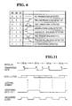
- Fig. 6 shows the generation of C-IN and the individual bits of STEP.
- the symbol L0 represents the least significant bit of LENGTH
- L6 represents the most significant bit.
- the first two lines of Fig. 6 show a division of LENGTH by 16 and the next two lines show a division by 32. Thus the least significant bit, of LENGTH, L0 does not appear in Fig. 6.
- the digital phase lock loop decoder 30 It is convenient at the present juncture to describe generally the operation of the digital phase lock loop decoder 30. This operation falls into three phases. When no data is being received, the signal CRS is inactive and the delay correction section 34 is continuously active to compensate for variations in the actual delays of the delay lines 52, 58, 62, Fig. 3A. This has the advantage that the decoder 30 can be implemented in environments where large absolute delay variations occur, for example due to temperature or power supply variations, or device-to-device variations in integrated circuit chips.
- the signal CRS When the reception of data is detected, the signal CRS becomes active and the training phase is entered.
- the training period continues for 48 bit times, as determined by the preamble timer section 36.
- three received data samples are utilized per bit time. These samples are taken using three clock signals, CLK 1, CLK 2 and CLK 3 having the same clock rate as the data rate (10 MHz).
- Each of the three clock signals has a 90° phase difference compared to the previous clock.
- the 90° phase shifts are effected by delaying the sample clocks by means of the calibrated delay lines 52 and 58 and a fixed, compensating delay 62.
- the three clock signals CLK 1, CLK 2 and CLK 3 can be regarded as generating a window, corresponding to the sampled signals Q1, Q2, and Q3 provided by the flip-flips 70, 74 and 78, Fig. 3B.
- the PLL 108 not only samples of the current window are utilized, but also samples for the immediately preceding window, to assist in determining whether the phase of the PLL reference clock (PLL CLOCK) is leading or trailing compared to the phase of the received data signal RD. This has the advantage, as compared with utilizing only the current window, of minimizing erroneous decisions which might be taken in the presence of a large amount of jitter on the received data transitions.
- the PLL decoder 30 trains by adjusting the phase of the PLL CLOCK signal until the phases of the REF CLK (CLK2) and the mid-bit transitions of the recorded data (RD) match.
- CLK2 the phases of the REF CLK
- RD recorded data
- the phase compare logic 86 determines whether the phase of REF CLOCK is leading or trailing. If the REF CLOCK phase leads, then the counter circuit 96 counts down. If the REF CLOCK phase trails, then the counter circuit 96 counts up. In order to determine the proper count direction, the phase compare logic 86 utilizes the three consecutive samples Q1, Q2, Q3, of the signal RD. The sample Q2 represents the value of RD at the rising edge of REF CLOCK.
- the sample Q3 represents the value of the signal RD 25 ns before the rising edge of REF CLOCK, and the sample Q1 equals the value of the signal RD 25 ns after the rising edge of REF CLOCK.
- the phase compare logic circuit 86 ignores transitions of the signal RD that do not occur within the window Q1-Q3. Under certain conditions, as will be explained, the count direction is dependent on both the current samples Q1, Q2, Q3 and the immediately previous samples Q10, Q20, Q30.
- the counter circuit 96 operates at its lowest, fixed rate, which is independent of the value of LENGTH.
- the delay correction section 34 can provide compensation for delay line variations occurring as a result of power supply and temperature fluctuations, and of device-to-device variations such as occur in integrated circuits.
- the delay correction section 34 is operative when the signal CRS is inactive.
- the delay correction section 34 utilizes for delay correction the 0-100 ns delay line circuit 52 which is located in the data/clock recovery section 32. This has the advantage of preventing errors which might result from small delay differences between corresponding cells in two delay lines, if separate delay lines were utilized in the delay correction section 34 and the data/clock recovery section 32.
- the delay circuit 134 is provided to compensate for the intrinsic delay of the delay line circuit 52.
- the delay circuit 134 has a delay equal to the intrinsic delay of the selector switch 176 (Fig. 4) in the delay line circuit 52.
- the 10 MHz clock signal is applied from the line 44 to the multitapped delay line 170 (Fig. 4) included in the delay line circuit 52.
- the output tap selected by the switch 176 has its signal provided on the output line 54 and hence via the line 133 to the phase comparator circuit 130, the other input 138 to which receives the delayed 10 MHz clock signal, delayed by the compensating delay circuit 134.
- the 10 MHz clock signal is also applied via the line 122 to the counter 120.
- the count output of the counter 120 is provided over the line 108 at this time via the multiplexer 104 and the line 106 to the address input of the switch 176 (Fig. 4) to select an associated one of the taps of the delay line 170 for connection over the lines 54, 133 to the phase comparator 130.
- the counter 120 is incremented and a further phase comparison is effected.
- the phase comparator 130 detects a phase match the value LENGTH in the counter 120 is latched into the latch circuit 142 and the counter 120 is reset to the start value S which is loaded in response to a signal applied through the OR gate 126.
- the latch circuit 142 always stores a value LENGTH which represents the number of delay cells 172 (Fig. 4) which provide a delay equal to the clock period of 100 ns, i.e. corresponding to a phase shift of 360°.
- the CRS signal becomes active, the current value of LENGTH stored in the latch circuit 142 is utilized for the data and clock recovery operation in the data/clock recovery section 32.
- the counter circuit 96 cycles between zero and the 7-bit value of LENGTH, corresponding to a PLL CLOCK phase shift of 360°.
- the data/clock recovery section 32 has three possible phase adjustment speeds.
- the adjustment speed is related to the magnitude of the difference between the RD (received data) signal and the REF CLOCK signal. For a larger phase difference, a higher adjustment speed is utilized.
- the window should be wider than the maximum expected jitter on the mid-bit transitions.
- the optimal width is 50 ns. This width allows a jitter amplitude of up to 25 ns on both sides of the intermediate and mid-bit transitions, yet permits the window still to achieve its purposes.
- the window is created by delaying the clock signal PLL CLOCK on the line 54 by 50 ns and by 25 ns, utilizing the delay line circuits 58 and 62.
- the delay values of the delay lines 58 and 62 are arranged to be independent of the absolute value of the delays of the delay cells constituting the delay lines. This is achieved as follows.
- the value of LENGTH, stored in the latch circuit 142 corresponds to a 360° phase shift or a 100 ns delay.
- the value LENGTH/2 corresponds to a 50 ns delay, and this value, via the 6-bit wide line 210, is applied as a six-bit input signal to the delay line 58.
- the value LENGTH/4 corresponds to a 25 ns delay, and this value is applied via the 5-bit wide line 212 as a five-bit input signal to the delay line 62.
- the delay circuit 66 is provided to compensate for the intrinsic delay in the delay line circuits 58, 62, that is, the intrinsic delay of the switches, corresponding to the switch 176, Fig. 4, which are provided in the delay line circuits 58, 62.
- the PLL CLOCK on the line 54 is delayed by the delay circuit 66 by this intrinsic delay, to provide the signal CLK 3.
- the PLL decoder adjusts the phase of PLL CLOCK and the mid-bit phases of REF CLOCK and the mid-bit transitions of the RD signal match, the effect of the intrinsic switch delay being compensated as described above.
- phase compare logic circuit 86 which includes a clocked storage element 220 having an 3-bit wide output line 222 connected to a logic circuit 224, which may be implemented as a state machine, and which receives the signals Q1, Q2, Q3 representing the current window samples from the lines 80, 82, 84.
- the storage element 220 applies the previous window samples Q10, Q20 and Q30 to the logic circuit 224 via the 3-bit wide line 222.
- Fig. 8 there is shown the interpretation of the window information. It will be appreciated the two transitions in a window, corresponding to the samples 010 and 101 will occur only if noise causes a spurious level shift.
- the logic circuit 224 implements Table 2. As is conventional, X represents a "don't care" state. Table 2 Q30 Q20 Q10 Q3 Q2 Q1 000 000 or 111 111 Illegal code. Inhibit count.
- Opposite stationary levels in the previous window and the current window provide no up/down information. Therefore, the PLL 108 is adjusted in a fixed direction (UP). Normally these codes can only occur at the start of a message when the PLL is completely off phase (stage A). However, it is possible that during subsequent stages of operation (e.g. PLL 108 is adjusting DOWN) an incidental 000 111 or 111 000 occurs due to a jitter peak. In that case it would be undesirable to adjust in the UP direction. The PLL should not adjust.
- a state machine which will be described later, with reference to Fig. 9, decides whether the 000 111 or 111 000 is incidental or not.
- the information in both windows is utilized.
- the direction of count U or D
- the direction of count is determined by considering first a jitter-free signal, adding 20 ns jitter to the transitions, listing all possible 6-bit codes for one transition in two windows and, using the 6-bit codes and the signal including jitter, and determining ranges of possible windows. The position of the possible ranges relative to the transitions of the jitter free signal determines the required direction of count.
- Table 4 shows a listing of all valid codes, and the resulting directions of count, for decoding in stages A, B and C.
- the state machine is part of the logic circuit 224 (Fig. 7) included in the phase compare logic circuit 86 (Fig. 3A).
- the state machine is controlled by the Q1, Q2, Q3 output signal shown in Fig. 8.
- the preamble timer section 36 provides an active signal INTEGR and stage D of the decoding operations is entered. During stage D, decoding is performed according to Table 5. Table 5 Q3 Q2 Q1 U/D INH 0 0 0 X 1 0 0 1 U 0 0 1 0 X 1 0 1 1 D 0 1 0 0 D 0 1 0 1 0 1 X 1 1 1 0 U 0 1 1 1 X 1
- the signal FINE controls the size of the incremental or decremental steps of the counter circuit 96.
- CMOS complementary metal-oxide-semiconductor
Abstract
Description
- This invention relates to digital phase lock loop decoders.
- The invention has a particular application to the decoding of Manchester coded data. In Manchester coded data a signal transition is present at each mid-cell location, the direction of the transition representing the value of the encoded binary bit.
- A digital phase lock loop decoder for decoding Manchester coded data is known from US Patent No. 4,584,695. This known decoder employs a multiphase driver clock circuit which provides clock signals which are phase-offset from one another. One clock output signal is used as the driver clock to provide a sample clock signal at four times the data rate or, in a fast clock mode, at eight times the data rate to determine whether the PLL reference clock is leading or lagging with respect to the received data signal. Thus, the known decoder has the disadvantage of needing relatively high rate clock signals, thereby rendering unsuitable the utilization of relatively lower speed, low cost implementation technologies, such as CMOS.
- It is an object of the present invention to provide a digital phase lock loop decoder in which the aforementioned disadvantage is alleviated.
- Therefore, according to the present invention, there is provided a digital phase lock loop decoder for decoding input data signals occurring at a predetermined nominal rate, characterized by clock signal supply means adapted to supply a first clock signal at said predetermined nominal rate, first delay line means adapted to delay said clock signal by a controllable delay time to provide a second clock signal, second delay line means adapted to receive said second clock signal and to provide a plurality of delayed clock signals having respective phased delay times relative to said second clock signal, sampling means responsive to said delayed clock signals and to said input data signals and adapted to provide a plurality of signal samples of said input data signals, phase compare logic means responsive to said second clock signal and to said plurality of signal samples and adapted to provide counter control signals adapted to control the operation of counter means, feedback means coupled between an output of said counter means and said first delay line means and adapted to control said controllable delay time, thereby controlling the phase of said second clock signal to correspond with the phase of a selected one of said plurality of delayed clock signal, and data output means coupled to said sampling means and adapted to provide decoded output data signals corresponding to said input data si nals.
- One embodiment of the present invention will now be described by way of example, with reference to the accompanying drawings, in which:-
- Fig. 1 shows waveform diagrams illustrative of Manchester encoded data;
- Fig. 2 is a block diagram of a data transmission system;
- Figs. 3A and 3B form a block diagram of a digital phase lock loop decoder according to the invention, for decoding Manchester encoded data;
- Fig. 4 is a block diagram of a delay line circuit, utilized in the decoder shown in Figs. 3A and 3B;
- Fig. 5 is a block diagram of a cyclic up/down counter utilized in the circuit shown in Figs. 3A and 3B;
- Fig. 6 is a table helpful in understanding the operation of the cyclic up/down counter;
- Fig. 7 is a block diagram of the phase compare logic circuit shown in Fig. 3B;
- Fig. 8 is a table showing the interpretation of window information;
- Fig. 9 is a state diagram for the FLAG signal;
- Fig. 10 is a state diagram for the FINE signal; and
- Fig. 11 shows waveforms illustrating the data recovery operation.
- Referring first to Fig. 1, the nature of a Manchester coded data signal will be described. Waveform A shown in Fig. 1 shows a periodic clock signal; waveform B shows a NRZ (nonreturn to zero) data signal, waveform C shows a corresponding Manchester coded data signal and line D shows the values of the data bits. It will be appreciated that the Manchester coded data signal C can be generated by the modulo-2 (exclusive-or) addition of the NRZ data signal B and the clock signal A. A Manchester coded signal consists of bit cells having a period equal to the data rate, the middle of each bit cell containing a transition which indicates the value of the data bit. Thus, a rising transition represents a "1" bit and a falling transition represents a "0" bit. Intermediate bit transitions between two bit cells occur only when two consecutive data bits are equal.
- Referring now to Fig. 2, there is shown a data transmission system in which input data on a
line 10 is applied to atransmitter 12 which converts the data to a Manchester coded signal for transmission over atransmission channel 14 to areceiver 16. Thereceiver 16 decodes the received Manchester coded signal to provide an output clock signal on aline 18 and an output data signal on aline 20. - In the preferred embodiment the
transmitter 12 utilizes a system clock signal (Fig. 1A), which is at a 10 MHz frequency, such that bit cells occur at 100 ns (100 nanosecond) intervals. However, noise and distortion introduced on thetransmission channel 14 will cause signal degradation, resulting in jitter on the mid-bit and intermediate bit transitions shown in Fig. 1C. Clearly, the maximum allowable jitter is from. +25 ns to -25 ns (50 ns peak to peak), since if the jitter amplitude exceeds 25 ns it will no longer be possible to distinguish mid-bit transitions from intermediate bit transitions. - In the preferred embodiment, the data is transmitted in the form of messages consisting of 62 bits of preamble, a two bit start of frame flag signal and a data field with a length of form 46 to 1500 data bytes. The 62 bit preamble is an alternating 1010 pattern which, when coded in Manchester code does not contain any intermediate bit transitions.
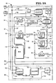
- Referring now to Figs. 3A and 3B, there is shown a Manchester
decoder 30 forming a portion of the receiver 16 (Fig. 2). Thedecoder 30 includes: a data/clock recovery section 32, which utilizes a digital PLL (phase lock loop) and a plurality of delay lines; adelay correction section 34 which controls an initial setting for the delay lines, as will be explained hereafter; and apreamble timer section 36 which times a training period corresponding to the first 48 bits of the 62 bit preamble portion of a received message. - The
decoder 30 receives the received data signal RD over aline 40, a carrier sense signal (CRS) over aline 42 which becomes active when energy is detected on the transmission channel 14 (Fig. 2) at the start of message reception, and a locally generated 10 MHz clock signal over aline 44. - The data/
clock recovery section 32 will first be described. The 10 MHzclock input line 44 is connected over aline 50 to a tappeddelay line unit 52 which has a selectable delay up to a maximum delay of 100 ns. The construction of thedelay line unit 52 will be described hereinafter with reference to Fig. 4. The output of thedelay line unit 52, on anoutput line 54, is a phase lock loop clock signal, referred to as the PLL CLOCK. By selecting an appropriate tap of thedelay line unit 52, the phase of the PLL clock signal is adjustable from 0° to 360°, corresponding to 0 ns up to 100 ns delay. - The
line 54 is connected via aline 56 to the input of adelay line unit 58, via aline 60 to the input of adelay unit 62, and via aline 64 to the input of adelay device 66. Thedelay line units delay line unit 52, to be described hereinafter. The output of thedelay line unit 58 is connected to aline 68, which is coupled to theclock output line 18, and which is also coupled to the clock input of flip-flop 70. The output of thedelay line unit 62 is connected to aline 72 which is connected to the clock input of a flip-flop 74. The output of thedelay device 66 is connected via aline 76 to the clock input of a flip-flop 78. The output signals on thelines flops RD signal input 40 which carries the received Manchester coded data and the flop-flops flops output lines output line 80 of the flip-flop 70 is coupled to theoutput data line 20. - The
output lines flops logic circuit 86, to be described hereinafter, which also receives as an input the PLL CLOCK signal via aline 88 connected to theline 54. - The phase compare
logic circuit 86 has threeoutput lines counter circuit 96, which also receives the PLL CLOCK signal via aline 98 coupled to theline 88, and an enabling signal INTEGR on aline 100 which is the output line of thepreamble timer section 36. A predetermined value, LENGTH is also provided to thecounter circuit 96, via aline 101 which is an output of thedelay correction section 34, and the carrier sense signal CRS is provided to thecounter circuit 96 vialine 102. - The 7-bit wide output count signal of the
counter circuit 96 is fed back via aline 103 to one input of amultiplexer 104, the output of which is connected over a 7-bitwide line 106 to thedelay line circuit 52. Themultiplexer 104 also receives a further 7-bit wide input, via aline 107, from thedelay correction section 34, and a select control input, via aline 110, which is connected to theline 42 on which the carrier sense signal CRS is provided. It will be appreciated that the data/clock recovery section 32 includes a digital phase lock loop, indicated generally by thereference 108. - The
delay correction section 34 will now be described. Thedelay correction section 34 includes acounter 120 which counts the 10 MHz clock signal supplied via aline 122 connected to theline 44. Thecounter 120 can be reset to a start value S, which is supplied from aregister 124, or may be hard-wired into the counter logic. Thecounter 120 is loaded with the start value S under the control of a LOAD signal provided on the output of anOR gate 126 which receives as inputs the carrier sense signal CRS, over aline 128 connected to theline 42, and a phase compare output signal from aphase comparator 130, over a line 132. - The
phase comparator 130 receives as inputs the output signal of thedelay line circuit 52, via aline 133, and the delayed 10 MHz clock signal via adelay circuit 134 which has an input connected via aline 136 to theline 44 and an output connected via aline 138 to thephase comparator 130. - The output of the
phase comparator 130 is also connected via aline 140 to alatch circuit 142 to effect the latching of the 7-bit wide output count signal of thecounter 120 into thelatch circuit 142. The value latched into thelatch circuit 142 is the value LENGTH, which value is then applied over a 7-bitwide line 146 as the output of thedelay correction section 34. - The
preamble timer section 36 will now be described. Thepreamble timer section 36 includes acounter 150 having a count input connected via aline 152 to theline 44 to receive to 10 MHz clock signal, and a clear input connected via aline 154 to receive the inverted carrier sense signal CRS. Thecounter 150 has a 6-bit output connected to a 6-bitwide output line 156 which is connected to adecoder 158. The output of thedecoder 158 is connected via aline 160 to the set input of a flag circuit 162, the output of which provides the aforementioned INTEGR signal on theline 100. The flag circuit 162 also receives a clear signal over aline 164 connected to receive the inverted carrier sense signal CRS on theline 44. - Referring now to Fig. 4, a circuit for implementing the
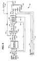
delay line circuit 52 will now be described. Thedelay line circuit 52 includes adelay line 170 including a plurality, N, ofdelay cells 172 referred to as individual delay cells 172-1, 172-2, ...-..., 172-N-1, 172 N, each cell being of identical construction and formed for example, in known manner, as a buffer cell or an AND gate, which may be implemented as CMOS circuits where thedecoder 30 is implemented in a CMOS technology integrated circuit chip. The 10 MHz clock signal on theline 50 is connected to the input of the first delay cell 172-1. The outputs of thedelay cells 172 are connected to an N-bitwide line 174, which is connected to the input of a 1 ofN selector switch 176, having an A-bit wide address supplied over theline 106. The output of theselector switch 176 is connected to theoutput line 54 of thedelay line circuit 52. It should be understood that a particular one of the N input lines is connected to theoutput line 54, in accordance with an address supplied on theline 106. - For the 0-100 ns
delay line 52, the value of N is 128 and the value of A is 7. Thus a 7-bit address selects one of 182 delay line taps to provide a delayed output on theline 54. If the value of the A-bit address is X, then the output of delay cell number X is connected to the output of theselector switch 176. - The
delay line circuits delay line circuit 52, and differ only in the values of the parameters N and A. Thus, for the 0-50 nsdelay line circuit 58, the value of N is 64, and the value of A = 6. For the 0-25 nsdelay line circuit 62, the value of N is 32 and the value of A is 5. - Referring now to Fig. 5, there is shown a block diagram of the cyclic up/down
counter circuit 96. Thecounter circuit 96 includes anincrement generator 180, which receives the control signals FINE, U/D, and INTEGR over thelines wide line 101. The increment generator generates a 10-bit wide STEP signal on a 10-bitwide output line 182, together with a CARRY IN (C-IN) signal on aline 184. Thelines adder circuit 186. Theadder circuit 186 provides a 10-bit wide output signal on a 10-bitwide line 188, together with a CARRY OUT signal on aline 190. Thelines overflow detection circuit 192, which also receives as inputs the 7-bit value of LENGTH from the 7-bit line 101 via a 7-bit line 194, and the signal U/D from theline 94 via aline 196. Thedetection circuit 192 provides a 10-bit wide output signal on a 10-bitwide line 198 to the data input of a 10-bit flip-flop block 200, which also receives as a clocking input the PLL CLOCK signal over theline 98, the INH signal over theline 92 as an inhibit signal, and the inverted carrier sense signal CRS from theline 102 as a reset signal. A 10-bitwide output line 202 is connected to afeedback line 204 which is an input to theadder 186. The seven most significant bit lines of theoutput line 202 are connected to the 7-bitwide line 103, to provide the signal PLL OUT which is fed back to themultiplexer 104, Fig. 3A. - With the above in mind, it will be appreciated that the cyclic up/down
counter circuit 96 is implemented as anadder 186 with its outputs fed back to a set of its inputs. Theadder 186 adds the output of the flip-flop block 200 to the 10-bit output value STEP of theincrement generator 180. Thus, at every PLL CLOCK period, the value of STEP is added to or subtracted from the counter output. When the signal U/D on theline 94 indicates UP, STEP is added to the counter output value, and when the signal U/D indicates DOWN, STEP is subtracted from the counter output. The internal data width of thecounter circuit 96 is 10 bits. However, the external interface utilizes only the seven most significant of these bits. A one step increase in the external 7-bit external output on theline 103 corresponds to a one tap increase in the delay of thedelay line 52, Fig. 3A, as will be more fully described hereinafter. - The result of the addition or subtraction in the
adder 186 is checked by the underflow/overflow detection circuit 192. If the value is smaller than all zeros, and U/D is DOWN, then the underflow condition occurs and the underflow/overflow detection circuit 192 will replace the result by the value of LENGTH, applied over theline 194. If the value is larger than LENGTH and U/D is UP, then the overflow condition occurs and the underflow/overflow detection circuit 192 will replace the result by all zeros. Summarizing, thecounter circuit 96 cycles between zero and LENGTH. - The INH input on the
line 92 is activated when the phase comparelogic circuit 86, Fig. 3B, is unable to make a valid UP or DOWN decision, for example as a result of noise on thetransmission channel 14. When the signal CRS is inactive, thecounter circuit 96 is reset. Thus thePLL 108 will be inactive when no data is being received over thetransmission channel 14. - It should be understood that the
counter circuit 96 is able to count at three different speeds, determined by the size of STEP. There are two fast speeds for the PLL 108 (Fig. 3A, 3B) during the training period, and one, lowest possible, speed, when thePLL 108 is locked after training. The value of STEP thus sets the step size to control the speed of thecounter circuit 96. The speed of thecounter circuit 96 during the training mode is independent of the absolute value of the delay cells in thedelay line 52, Fig. 3A. This is achieved by theincrement generator 180 being effective during the training period by utilizing the value of LENGTH in the generation of STEP, as shown in Table 1. When thePLL 108 is locked, thecounter circuit 96 will count at the lowest possible speed, which is independent of the value of LENGTH.TABLE 1 FINE INTEGR U/ D STEP 0 0 U + LENGTH/16 0 0 D - LENGTH/16 1 0 U + LENGTH/32 1 0 D - LENGTH/32 X 1 U + 1/8 X 1 D - 1/8 - Negative values (2's complements) of STEP are obtained by inverting all ten bits and activating the CARRY IN signal (C-IN) on the
line 184. Fig. 6 shows the generation of C-IN and the individual bits of STEP. The symbol L0 represents the least significant bit of LENGTH, and L6 represents the most significant bit. The first two lines of Fig. 6 show a division of LENGTH by 16 and the next two lines show a division by 32. Thus the least significant bit, of LENGTH, L0 does not appear in Fig. 6. - It is convenient at the present juncture to describe generally the operation of the digital phase
lock loop decoder 30. This operation falls into three phases. When no data is being received, the signal CRS is inactive and thedelay correction section 34 is continuously active to compensate for variations in the actual delays of thedelay lines decoder 30 can be implemented in environments where large absolute delay variations occur, for example due to temperature or power supply variations, or device-to-device variations in integrated circuit chips. - When the reception of data is detected, the signal CRS becomes active and the training phase is entered. The training period continues for 48 bit times, as determined by the
preamble timer section 36. During the training period three received data samples are utilized per bit time. These samples are taken using three clock signals,CLK 1,CLK 2 andCLK 3 having the same clock rate as the data rate (10 MHz). Each of the three clock signals has a 90° phase difference compared to the previous clock. The 90° phase shifts are effected by delaying the sample clocks by means of the calibrateddelay lines delay 62. The threeclock signals CLK 1,CLK 2 andCLK 3 can be regarded as generating a window, corresponding to the sampled signals Q1, Q2, and Q3 provided by the flip-flips PLL 108 not only samples of the current window are utilized, but also samples for the immediately preceding window, to assist in determining whether the phase of the PLL reference clock (PLL CLOCK) is leading or trailing compared to the phase of the received data signal RD. This has the advantage, as compared with utilizing only the current window, of minimizing erroneous decisions which might be taken in the presence of a large amount of jitter on the received data transitions. - Thus, it will be appreciated that the
PLL decoder 30 trains by adjusting the phase of the PLL CLOCK signal until the phases of the REF CLK (CLK2) and the mid-bit transitions of the recorded data (RD) match. When the phases match, thePLL 108 is locked. The phase comparelogic 86 determines whether the phase of REF CLOCK is leading or trailing. If the REF CLOCK phase leads, then thecounter circuit 96 counts down. If the REF CLOCK phase trails, then thecounter circuit 96 counts up. In order to determine the proper count direction, the phase comparelogic 86 utilizes the three consecutive samples Q1, Q2, Q3, of the signal RD. The sample Q2 represents the value of RD at the rising edge of REF CLOCK. The sample Q3 represents the value of thesignal RD 25 ns before the rising edge of REF CLOCK, and the sample Q1 equals the value of thesignal RD 25 ns after the rising edge of REF CLOCK. The phase comparelogic circuit 86 ignores transitions of the signal RD that do not occur within the window Q1-Q3. Under certain conditions, as will be explained, the count direction is dependent on both the current samples Q1, Q2, Q3 and the immediately previous samples Q10, Q20, Q30. - During the third phase of operation, after the training period, the
counter circuit 96 operates at its lowest, fixed rate, which is independent of the value of LENGTH. - The operation of the
delay correction section 34 will now be described in more detail, with reference to Fig. 3A. Thedelay correction section 34 can provide compensation for delay line variations occurring as a result of power supply and temperature fluctuations, and of device-to-device variations such as occur in integrated circuits. As previously mentioned, thedelay correction section 34 is operative when the signal CRS is inactive. Note first that thedelay correction section 34 utilizes for delay correction the 0-100 nsdelay line circuit 52 which is located in the data/clock recovery section 32. This has the advantage of preventing errors which might result from small delay differences between corresponding cells in two delay lines, if separate delay lines were utilized in thedelay correction section 34 and the data/clock recovery section 32. It should further be noted that thedelay circuit 134 is provided to compensate for the intrinsic delay of thedelay line circuit 52. Thus thedelay circuit 134 has a delay equal to the intrinsic delay of the selector switch 176 (Fig. 4) in thedelay line circuit 52. - The 10 MHz clock signal is applied from the
line 44 to the multitapped delay line 170 (Fig. 4) included in thedelay line circuit 52. The output tap selected by theswitch 176 has its signal provided on theoutput line 54 and hence via theline 133 to thephase comparator circuit 130, theother input 138 to which receives the delayed 10 MHz clock signal, delayed by the compensatingdelay circuit 134. The 10 MHz clock signal is also applied via theline 122 to thecounter 120. The count output of thecounter 120 is provided over theline 108 at this time via themultiplexer 104 and theline 106 to the address input of the switch 176 (Fig. 4) to select an associated one of the taps of thedelay line 170 for connection over thelines phase comparator 130. As long as no phase match is detected, thecounter 120 is incremented and a further phase comparison is effected. When thephase comparator 130 detects a phase match the value LENGTH in thecounter 120 is latched into thelatch circuit 142 and thecounter 120 is reset to the start value S which is loaded in response to a signal applied through theOR gate 126. Thus thelatch circuit 142 always stores a value LENGTH which represents the number of delay cells 172 (Fig. 4) which provide a delay equal to the clock period of 100 ns, i.e. corresponding to a phase shift of 360°. When the CRS signal becomes active, the current value of LENGTH stored in thelatch circuit 142 is utilized for the data and clock recovery operation in the data/clock recovery section 32. - Thus, during the next, phase of operation, which is the training period, the
counter circuit 96 cycles between zero and the 7-bit value of LENGTH, corresponding to a PLL CLOCK phase shift of 360°. - As previously mentioned the data/
clock recovery section 32 has three possible phase adjustment speeds. The adjustment speed is related to the magnitude of the difference between the RD (received data) signal and the REF CLOCK signal. For a larger phase difference, a higher adjustment speed is utilized. Once thePLL 108 is locked and the phases of the REF CLOCK and the RD mid-bit transitions match, the centre of the window defined by the samples Q1-Q3 is positioned on the mid-bit transitions. The window should capture every mid-bit transition and should prevent the PLL from locking onto intermediate bit transitions which may occur during data reception. The width of the window is determined by the object of achieving both these purposes. To prevent intermediate bit transitions from entering the window, the window should be as narrow as possible. To capture every mid-bit transition, the window should be wider than the maximum expected jitter on the mid-bit transitions. In the preferred embodiment, the optimal width is 50 ns. This width allows a jitter amplitude of up to 25 ns on both sides of the intermediate and mid-bit transitions, yet permits the window still to achieve its purposes. After the first 48 preamble bits as counted by thepreamble timer 36, thepreamble timer 36 signals the end of the training period, and thePLL 108 is locked, with the phase adjustment being made at the lowest speed. - It will now be appreciated that the window is created by delaying the clock signal PLL CLOCK on the
line 54 by 50 ns and by 25 ns, utilizing thedelay line circuits delay lines latch circuit 142, corresponds to a 360° phase shift or a 100 ns delay. Thus, the value LENGTH/2 corresponds to a 50 ns delay, and this value, via the 6-bitwide line 210, is applied as a six-bit input signal to thedelay line 58. The value LENGTH/4 corresponds to a 25 ns delay, and this value is applied via the 5-bitwide line 212 as a five-bit input signal to thedelay line 62. It will be appreciated that thedelay circuit 66 is provided to compensate for the intrinsic delay in thedelay line circuits switch 176, Fig. 4, which are provided in thedelay line circuits line 54 is delayed by thedelay circuit 66 by this intrinsic delay, to provide thesignal CLK 3. The PLL decoder adjusts the phase of PLL CLOCK and the mid-bit phases of REF CLOCK and the mid-bit transitions of the RD signal match, the effect of the intrinsic switch delay being compensated as described above. - Referring briefly to Fig. 7, there is shown a block diagram of the phase compare
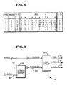
logic circuit 86, which includes a clockedstorage element 220 having an 3-bitwide output line 222 connected to alogic circuit 224, which may be implemented as a state machine, and which receives the signals Q1, Q2, Q3 representing the current window samples from thelines storage element 220 applies the previous window samples Q10, Q20 and Q30 to thelogic circuit 224 via the 3-bitwide line 222. - Referring now to Fig. 8, there is shown the interpretation of the window information. It will be appreciated the two transitions in a window, corresponding to the
samples 010 and 101 will occur only if noise causes a spurious level shift. - There are four stages of operation for the data/clock recovery section 32:-
- A. Adjust the
PLL 108 until a mid-bit transition is captured by the window, using STEP = LENGTH/16. - B. Adjust the
PLL 108 until mid-bit transitions are captured by two consecutive windows, using STEP = LENGTH/16. - C. Adjust the
PLL 108 until the mean value of the jitter is positioned in the middle of the window, using STEP = LENGTH/32 - D. Adjust the
PLL 108 only to compensate for any frequency deviation of the received data. This stage is entered after the 48-bitpreamble timer section 36 has timed out. The value of STEP = 1/8. - During the first 48 preamble bits, when the
PLL 108 is not yet in lock, not every window captures a transition. Therefore, the previous window information, referred to as Q10, Q20, Q30, and generated by thestorage element 220, Fig. 7, is also used. Note that, by using the samples of both the current and previous windows, the reliability of decisions in the presence of jitter on the RD signal transitions is significantly increased. During the first 48 preamble bits, corresponding to stages A, B and C, thelogic circuit 224 implements Table 2. As is conventional, X represents a "don't care" state.Table 2 Q30 Q20 Q10 Q3 Q2 Q1 000 000 or 111 111 Illegal code. Inhibit count. INH = 1 , U/D = X 000 111 or 111 000 Stage A Adjust PLL (always up) until transition is captured. INH = 0 , U/D = up 001 001 or 001 011 Illegal codes. Equal polarity transitions detected in previous and current window. Inhibit count. INH = 1 , U/D = X 011 001 or 011 011 100 100 or 100 110 110 100 or 110 110 001 100 or 001 110 Opposite result transitions detected in previous and current window. Use information from current window only. (See Table 3) 011 100 or 011 110 100 001 or 100 011 110 001 or 110 011 000 001 or 000 011 One transition in two consecutive windows detected. Use information from both windows.(See Table 4) 000 100 or 000 110 111 001 or 111 011 111 100 or 111 110 001 000 or 011 000 100 000 or 110 000 001 111 or 011 111 100 111 or 110 111 - Opposite stationary levels in the previous window and the current window (000 111 or 111 000) provide no up/down information. Therefore, the
PLL 108 is adjusted in a fixed direction (UP). Normally these codes can only occur at the start of a message when the PLL is completely off phase (stage A). However, it is possible that during subsequent stages of operation (e.g.PLL 108 is adjusting DOWN) an incidental 000 111 or 111 000 occurs due to a jitter peak. In that case it would be undesirable to adjust in the UP direction. The PLL should not adjust. A state machine, which will be described later, with reference to Fig. 9, decides whether the 000 111 or 111 000 is incidental or not. In case the code is identified as incidental, inhibit count will be forced active (INH = 1). In case of opposite transitions being detected in the previous and current window only the current window is utilized. In that case the current window is decoded according to Table 3.Table 3 Q3 Q2 Q1 U/ D INH 0 0 1 U 0 0 1 1 D 0 1 0 0 D 0 1 1 0 U 0 - If one window detects a transition and the other does not, the information in both windows is utilized. There are 16 possible cases of one transition in two consecutive windows, and the direction of count (U or D) is determined by considering first a jitter-free signal, adding 20 ns jitter to the transitions, listing all possible 6-bit codes for one transition in two windows and, using the 6-bit codes and the signal including jitter, and determining ranges of possible windows. The position of the possible ranges relative to the transitions of the jitter free signal determines the required direction of count. Table 4 shows a listing of all valid codes, and the resulting directions of count, for decoding in stages A, B and C.

- In Table 4, it should be appreciated that cases of two transitions in a single window, which are illegal codes, are not shown, and are always decoded into U/D = X, INH = 1.
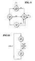
- Also, the decoding of the codes 000 111 and 111 000, which are shown in Table 4 as U/D = U and INH = 0, is effected by a state machine having the state diagram shown in Fig. 9. The state machine is part of the logic circuit 224 (Fig. 7) included in the phase compare logic circuit 86 (Fig. 3A). The output of the state machine, which is the signal FLAG, indicates whether the code was incidental or not. If FLAG = 1, then the code is incidental. The state machine is controlled by the Q1, Q2, Q3 output signal shown in Fig. 8. The signal FLAG is set by a non-inhibited DOWN (U/D = D and INH = 0). It is reset by three consecutive DOWN signals or INH signals. In the state diagram of Fig. 9, D0 means U/D = D and INH = 0. The state machine steps every PLL CLOCK signal. If the 000 111 or 111 000 code is incidential, i.e. FLAG = 1, then INH is forced active. Otherwise, the INH signal is passed through.
- After the first 48 preamble bits, the
preamble timer section 36 provides an active signal INTEGR and stage D of the decoding operations is entered. During stage D, decoding is performed according to Table 5.Table 5 Q3 Q2 Q1 U/ D INH 0 0 0 X 1 0 0 1 U 0 0 1 0 X 1 0 1 1 D 0 1 0 0 D 0 1 0 1 X 1 1 1 0 U 0 1 1 1 X 1 - The signal FINE, on
line 90, Figs. 3B and 5, controls the size of the incremental or decremental steps of thecounter circuit 96. The signal FINE is also generated by a state machine included in the logic circuit 224 (Fig. 7). The state diagram of this state machine is shown in Fig. 10. The signal FINE is set if the previous and the current window both contain a valid transition. The signal FINE is reset between messages when CRS is inactive (CRS = 0). - The data receiving operation will now be described, with reference to Fig. 11. This takes place when the
PLL 108 is locked. As previously mentioned, in Manchester code the value of a data bit is indicated by the polarity of the mid-bit transition. A rising mid-bit transition represents a one, a falling transition represents a zero. Thus, the second half of a bit cell has the same value as the Manchester encoded data bit. Data recovery is effected by latching the second half of a Manchester bit cell. The optimal latching moment is determined by the jitter extremes of the mid-bit transition and the following intermediate transition. In the worst case the mid-bit transition has a theoretical maximum jitter of + 25 ns and is followed by an intermediate transition having a - 25 ns jitter. Both transitions occur at the same moment in time. Should less than +/- 25 ns jitter be allowed, e.g. +/- 24 ns then there is a 2 ns period during which the data is valid. The optimum data latch period, i.e. the middle of this 2 ns, period is 25 ns after the occurrence of the mid-bit transition (3/4 of a bit cell, Fig. 11). The output of thedelay line circuit 58, Fig. 3A, which is CLK1, samples the RD (received data) signal 25 ns after the occurrences of the mid-bit transition, so Q1 equals the recovered data. - Thus, there has been described a digital phase lock loop decoder for decoding Manchester coded data which has the advantage of utilizing a clock signal that has a frequency equal to the data rate, thereby avoiding the need for high frequency sampling clock signal. This has the advantage that the decoder can be implemented in relatively low cost, reliable, low power technologies, such as CMOS.
Claims (12)
Applications Claiming Priority (2)
| Application Number | Priority Date | Filing Date | Title |
|---|---|---|---|
| GB898924202A GB8924202D0 (en) | 1989-10-27 | 1989-10-27 | Digital phase lock loop decoder |
| GB8924202 | 1989-10-27 |
Publications (3)
| Publication Number | Publication Date |
|---|---|
| EP0425302A2 true EP0425302A2 (en) | 1991-05-02 |
| EP0425302A3 EP0425302A3 (en) | 1994-02-23 |
| EP0425302B1 EP0425302B1 (en) | 1997-08-06 |
Family
ID=10665260
Family Applications (1)
| Application Number | Title | Priority Date | Filing Date |
|---|---|---|---|
| EP90311758A Expired - Lifetime EP0425302B1 (en) | 1989-10-27 | 1990-10-26 | Digital phase lock loop decoder suitable for Manchester codes |
Country Status (5)
| Country | Link |
|---|---|
| US (1) | US5003562A (en) |
| EP (1) | EP0425302B1 (en) |
| CA (1) | CA2026323C (en) |
| DE (1) | DE69031205T2 (en) |
| GB (1) | GB8924202D0 (en) |
Cited By (6)
| Publication number | Priority date | Publication date | Assignee | Title |
|---|---|---|---|---|
| WO1997032416A1 (en) * | 1996-02-28 | 1997-09-04 | Advanced Micro Devices, Inc. | Digital phase lock loop and system for digital clock recovery |
| WO1998044689A1 (en) * | 1997-03-31 | 1998-10-08 | Sun Microsystems, Inc. | Circuit for detecting and decoding phase encoded digital serial data |
| EP0930713A1 (en) * | 1997-12-04 | 1999-07-21 | STMicroelectronics S.r.l. | Decoding of a biphase modulated bitstream and relative selfsynchronizing frequency divider with noninteger ratio |
| DE19813965C1 (en) * | 1998-03-28 | 1999-08-19 | Telefunken Microelectron | Digital data pulse transmission method |
| US6060929A (en) * | 1996-09-20 | 2000-05-09 | Konica Corporation | Signal delay apparatus |
| EP1315304A2 (en) * | 2001-11-16 | 2003-05-28 | Philips Intellectual Property & Standards GmbH | Receiver circuit for communications signals |
Families Citing this family (25)
| Publication number | Priority date | Publication date | Assignee | Title |
|---|---|---|---|---|
| US5168511A (en) * | 1990-10-22 | 1992-12-01 | Berkeley Varitronics Systems, Inc. | Manchester data recorder with synchronously adjustable clock |
| EP0523885A1 (en) * | 1991-07-15 | 1993-01-20 | National Semiconductor Corporation | Phase detector for very high frequency clock and data recovery circuits |
| US5239561A (en) * | 1991-07-15 | 1993-08-24 | National Semiconductor Corporation | Phase error processor |
| US5271040A (en) * | 1991-12-20 | 1993-12-14 | Vlsi Technology, Inc. | Phase detector circuit |
| US5533072A (en) * | 1993-11-12 | 1996-07-02 | International Business Machines Corporation | Digital phase alignment and integrated multichannel transceiver employing same |
| US5594763A (en) * | 1995-06-06 | 1997-01-14 | Cirrus Logic, Inc. | Fast synchronizing digital phase-locked loop for recovering clock information from encoded data |
| US5726650A (en) * | 1995-06-07 | 1998-03-10 | Silicon Systems, Inc. | Adaptive manchester decoding with adjustable delay and power saving mode |
| US5892631A (en) * | 1995-09-08 | 1999-04-06 | Seagate Technology, Inc. | Method and an arrangement for detecting state transitions in a read signal during a bit cell timing window |
| GB9809450D0 (en) * | 1998-05-01 | 1998-07-01 | Wandel & Goltermann Limited | Jitter measurement |
| DE10007783A1 (en) | 2000-02-21 | 2001-08-23 | Rohde & Schwarz | Method and arrangement for data and clock recovery in a biphase-coded data signal |
| US6868504B1 (en) * | 2000-08-31 | 2005-03-15 | Micron Technology, Inc. | Interleaved delay line for phase locked and delay locked loops |
| US6987824B1 (en) * | 2000-09-21 | 2006-01-17 | International Business Machines Corporation | Method and system for clock/data recovery for self-clocked high speed interconnects |
| US7026850B2 (en) * | 2001-05-21 | 2006-04-11 | Acuid Corporation Limited | Programmable self-calibrating vernier and method |
| US7613263B2 (en) * | 2003-03-04 | 2009-11-03 | Altera Corporation | Clock and data recovery method and apparatus |
| US20040228411A1 (en) * | 2003-05-12 | 2004-11-18 | Sony Corporation | Method and system for decoder clock control in presence of jitter |
| US7751436B2 (en) * | 2005-05-24 | 2010-07-06 | Sony Corporation | System and method for dynamically establishing PLL speed based on receive buffer data accumulation for streaming video |
| US7692598B1 (en) | 2005-10-26 | 2010-04-06 | Niitek, Inc. | Method and apparatus for transmitting and receiving time-domain radar signals |
| JP2008066879A (en) * | 2006-09-05 | 2008-03-21 | Ricoh Co Ltd | Oversampling circuit, and oversampling method |
| US9316729B2 (en) * | 2007-05-25 | 2016-04-19 | Niitek, Inc. | Systems and methods for providing trigger timing |
| US7649492B2 (en) * | 2007-05-25 | 2010-01-19 | Niitek, Inc. | Systems and methods for providing delayed signals |
| US7652619B1 (en) | 2007-05-25 | 2010-01-26 | Niitek, Inc. | Systems and methods using multiple down-conversion ratios in acquisition windows |
| US7675454B2 (en) * | 2007-09-07 | 2010-03-09 | Niitek, Inc. | System, method, and computer program product providing three-dimensional visualization of ground penetrating radar data |
| US8207885B2 (en) * | 2007-09-19 | 2012-06-26 | Niitek, Inc. | Adjustable pulse width ground penetrating radar |
| US8355478B1 (en) | 2009-05-29 | 2013-01-15 | Honeywell International Inc. | Circuit for aligning clock to parallel data |
| WO2011004580A1 (en) * | 2009-07-06 | 2011-01-13 | パナソニック株式会社 | Clock data recovery circuit |
Citations (5)
| Publication number | Priority date | Publication date | Assignee | Title |
|---|---|---|---|---|
| US4584695A (en) * | 1983-11-09 | 1986-04-22 | National Semiconductor Corporation | Digital PLL decoder |
| EP0240232A2 (en) * | 1986-04-01 | 1987-10-07 | Hewlett-Packard Company | Digital phase lock loop |
| US4788605A (en) * | 1987-03-30 | 1988-11-29 | Honeywell Inc. | Receive Manchester clock circuit |
| US4789996A (en) * | 1988-01-28 | 1988-12-06 | Siemens Transmission Systems, Inc. | Center frequency high resolution digital phase-lock loop circuit |
| EP0317159A2 (en) * | 1987-11-19 | 1989-05-24 | AT&T Corp. | Clock recovery arrangement |
Family Cites Families (9)
| Publication number | Priority date | Publication date | Assignee | Title |
|---|---|---|---|---|
| DE2945331C2 (en) * | 1979-11-09 | 1984-05-30 | Nixdorf Computer Ag, 4790 Paderborn | Device in a signal or data processing system for setting a signal processing circuit |
| US4709170A (en) * | 1984-08-20 | 1987-11-24 | National Semiconductor Corp. | Subnanosecond programmable phase shifter for a high frequency digital PLL |
| JPS6194429A (en) * | 1984-10-15 | 1986-05-13 | Nec Corp | Phase synchronizing circuit |
| US4627080A (en) * | 1984-11-23 | 1986-12-02 | At&T Bell Laboratories | Adaptive timing circuit |
| US4795985A (en) * | 1986-04-01 | 1989-01-03 | Hewlett-Packard Company | Digital phase lock loop |
| JPH0770991B2 (en) * | 1986-08-27 | 1995-07-31 | 日本電気株式会社 | Clock reproduction circuit |
| FR2604043B1 (en) * | 1986-09-17 | 1993-04-09 | Cit Alcatel | DEVICE FOR RECORDING ONE OR MORE BINARY DATA TRAINS OF IDENTICAL OR SUB-MULTIPLE RATES ON A SYNCHRONOUS CLOCK REFERENCE SIGNAL |
| US4841551A (en) * | 1987-01-05 | 1989-06-20 | Grumman Aerospace Corporation | High speed data-clock synchronization processor |
| DE3855342T2 (en) * | 1987-10-01 | 1997-01-23 | Sharp Kk | Digital phase locked loop arrangement |
-
1989
- 1989-10-27 GB GB898924202A patent/GB8924202D0/en active Pending
-
1990
- 1990-03-14 US US07/493,546 patent/US5003562A/en not_active Expired - Lifetime
- 1990-09-27 CA CA002026323A patent/CA2026323C/en not_active Expired - Fee Related
- 1990-10-26 DE DE69031205T patent/DE69031205T2/en not_active Expired - Fee Related
- 1990-10-26 EP EP90311758A patent/EP0425302B1/en not_active Expired - Lifetime
Patent Citations (5)
| Publication number | Priority date | Publication date | Assignee | Title |
|---|---|---|---|---|
| US4584695A (en) * | 1983-11-09 | 1986-04-22 | National Semiconductor Corporation | Digital PLL decoder |
| EP0240232A2 (en) * | 1986-04-01 | 1987-10-07 | Hewlett-Packard Company | Digital phase lock loop |
| US4788605A (en) * | 1987-03-30 | 1988-11-29 | Honeywell Inc. | Receive Manchester clock circuit |
| EP0317159A2 (en) * | 1987-11-19 | 1989-05-24 | AT&T Corp. | Clock recovery arrangement |
| US4789996A (en) * | 1988-01-28 | 1988-12-06 | Siemens Transmission Systems, Inc. | Center frequency high resolution digital phase-lock loop circuit |
Cited By (12)
| Publication number | Priority date | Publication date | Assignee | Title |
|---|---|---|---|---|
| WO1997032416A1 (en) * | 1996-02-28 | 1997-09-04 | Advanced Micro Devices, Inc. | Digital phase lock loop and system for digital clock recovery |
| US5812619A (en) * | 1996-02-28 | 1998-09-22 | Advanced Micro Devices, Inc. | Digital phase lock loop and system for digital clock recovery |
| US6060929A (en) * | 1996-09-20 | 2000-05-09 | Konica Corporation | Signal delay apparatus |
| WO1998044689A1 (en) * | 1997-03-31 | 1998-10-08 | Sun Microsystems, Inc. | Circuit for detecting and decoding phase encoded digital serial data |
| US6148038A (en) * | 1997-03-31 | 2000-11-14 | Sun Microsystems, Inc. | Circuit for detecting and decoding phase encoded digital serial data |
| EP0930713A1 (en) * | 1997-12-04 | 1999-07-21 | STMicroelectronics S.r.l. | Decoding of a biphase modulated bitstream and relative selfsynchronizing frequency divider with noninteger ratio |
| US6487263B1 (en) | 1997-12-04 | 2002-11-26 | Stmicroelectronics S.R.L. | Decoding of a biphase modulated bitstream and relative self-synchronizing frequency divider with noninteger ratio |
| DE19813965C1 (en) * | 1998-03-28 | 1999-08-19 | Telefunken Microelectron | Digital data pulse transmission method |
| US6249558B1 (en) | 1998-03-28 | 2001-06-19 | Temic Telefunken Microeletronic Gmbh | Method for transmitting digital data impulses |
| EP1315304A2 (en) * | 2001-11-16 | 2003-05-28 | Philips Intellectual Property & Standards GmbH | Receiver circuit for communications signals |
| CN100438350C (en) * | 2001-11-16 | 2008-11-26 | Nxp股份有限公司 | Receiving circuit for receiving information signal |
| EP1315304B1 (en) * | 2001-11-16 | 2009-10-21 | Nxp B.V. | Receiver circuit for communications signals |
Also Published As
| Publication number | Publication date |
|---|---|
| EP0425302A3 (en) | 1994-02-23 |
| DE69031205T2 (en) | 1998-01-29 |
| CA2026323A1 (en) | 1991-04-28 |
| DE69031205D1 (en) | 1997-09-11 |
| GB8924202D0 (en) | 1989-12-13 |
| US5003562A (en) | 1991-03-26 |
| CA2026323C (en) | 1994-09-06 |
| EP0425302B1 (en) | 1997-08-06 |
Similar Documents
| Publication | Publication Date | Title |
|---|---|---|
| EP0425302B1 (en) | Digital phase lock loop decoder suitable for Manchester codes | |
| EP0317159B1 (en) | Clock recovery arrangement | |
| US5452333A (en) | Digital jitter correction method and signal preconditioner | |
| US7099400B2 (en) | Multi-level pulse amplitude modulation receiver | |
| US4608702A (en) | Method for digital clock recovery from Manchester-encoded signals | |
| US5903605A (en) | Jitter detection method and apparatus | |
| US6760389B1 (en) | Data recovery for non-uniformly spaced edges | |
| EP0326007A2 (en) | Center frequency high resolution digital phase-loop circuit | |
| US4847870A (en) | High resolution digital phase-lock loop circuit | |
| JPH08163117A (en) | Bit phase synchronizing circuit | |
| US5040193A (en) | Receiver and digital phase-locked loop for burst mode data recovery | |
| US5898734A (en) | Symbol determining method and apparatus | |
| US6389090B2 (en) | Digital clock/data signal recovery method and apparatus | |
| CA1294334C (en) | Digital data separator | |
| US5859551A (en) | Digital PLL circuit | |
| US4682343A (en) | Processing circuit with asymmetry corrector and convolutional encoder for digital data | |
| US5297164A (en) | Digital communications systems | |
| EP0162505B1 (en) | Arrangement for generating a clock signal | |
| US4628519A (en) | Digital phase-locked loop circuit | |
| JP2891535B2 (en) | Digital phase locked loop decoder | |
| US5396522A (en) | Method and apparatus for clock synchronization with information received by a radio receiver | |
| US4775989A (en) | Timing phase detector circuit | |
| US5479456A (en) | Automatic false synchronization correction mechanism for biphase-modulated signal reception | |
| US20070069927A1 (en) | Method of transmitting a serial bit-stream and electronic transmitter for transmitting a serial bit-stream | |
| KR100300947B1 (en) | Method and device for excluding error packet in data communication system |
Legal Events
| Date | Code | Title | Description |
|---|---|---|---|
| PUAI | Public reference made under article 153(3) epc to a published international application that has entered the european phase |
Free format text: ORIGINAL CODE: 0009012 |
|
| AK | Designated contracting states |
Kind code of ref document: A2 Designated state(s): DE FR GB |
|
| PUAL | Search report despatched |
Free format text: ORIGINAL CODE: 0009013 |
|
| AK | Designated contracting states |
Kind code of ref document: A3 Designated state(s): DE FR GB |
|
| 17P | Request for examination filed |
Effective date: 19940816 |
|
| RAP1 | Party data changed (applicant data changed or rights of an application transferred) |
Owner name: NCR INTERNATIONAL INC. |
|
| RAP1 | Party data changed (applicant data changed or rights of an application transferred) |
Owner name: AT&T GLOBAL INFORMATION SOLUTIONS INTERNATIONAL IN |
|
| 17Q | First examination report despatched |
Effective date: 19960321 |
|
| RAP1 | Party data changed (applicant data changed or rights of an application transferred) |
Owner name: NCR INTERNATIONAL, INC. |
|
| GRAG | Despatch of communication of intention to grant |
Free format text: ORIGINAL CODE: EPIDOS AGRA |
|
| GRAH | Despatch of communication of intention to grant a patent |
Free format text: ORIGINAL CODE: EPIDOS IGRA |
|
| GRAH | Despatch of communication of intention to grant a patent |
Free format text: ORIGINAL CODE: EPIDOS IGRA |
|
| GRAA | (expected) grant |
Free format text: ORIGINAL CODE: 0009210 |
|
| AK | Designated contracting states |
Kind code of ref document: B1 Designated state(s): DE FR GB |
|
| REF | Corresponds to: |
Ref document number: 69031205 Country of ref document: DE Date of ref document: 19970911 |
|
| ET | Fr: translation filed | ||
| PLBE | No opposition filed within time limit |
Free format text: ORIGINAL CODE: 0009261 |
|
| STAA | Information on the status of an ep patent application or granted ep patent |
Free format text: STATUS: NO OPPOSITION FILED WITHIN TIME LIMIT |
|
| 26N | No opposition filed | ||
| REG | Reference to a national code |
Ref country code: GB Ref legal event code: IF02 |
|
| PGFP | Annual fee paid to national office [announced via postgrant information from national office to epo] |
Ref country code: GB Payment date: 20030929 Year of fee payment: 14 |
|
| REG | Reference to a national code |
Ref country code: GB Ref legal event code: 746 Effective date: 20030924 |
|
| PGFP | Annual fee paid to national office [announced via postgrant information from national office to epo] |
Ref country code: FR Payment date: 20031031 Year of fee payment: 14 |
|
| PGFP | Annual fee paid to national office [announced via postgrant information from national office to epo] |
Ref country code: DE Payment date: 20031201 Year of fee payment: 14 |
|
| REG | Reference to a national code |
Ref country code: FR Ref legal event code: D6 |
|
| PG25 | Lapsed in a contracting state [announced via postgrant information from national office to epo] |
Ref country code: GB Free format text: LAPSE BECAUSE OF NON-PAYMENT OF DUE FEES Effective date: 20041026 |
|
| PG25 | Lapsed in a contracting state [announced via postgrant information from national office to epo] |
Ref country code: DE Free format text: LAPSE BECAUSE OF NON-PAYMENT OF DUE FEES Effective date: 20050503 |
|
| GBPC | Gb: european patent ceased through non-payment of renewal fee |
Effective date: 20041026 |
|
| PG25 | Lapsed in a contracting state [announced via postgrant information from national office to epo] |
Ref country code: FR Free format text: LAPSE BECAUSE OF NON-PAYMENT OF DUE FEES Effective date: 20050630 |
|
| REG | Reference to a national code |
Ref country code: FR Ref legal event code: ST |