EP0410395A2 - Photoelectric conversion device having an improved illuminating system, and information processing apparatus equipped therewith - Google Patents
Photoelectric conversion device having an improved illuminating system, and information processing apparatus equipped therewith Download PDFInfo
- Publication number
- EP0410395A2 EP0410395A2 EP90114196A EP90114196A EP0410395A2 EP 0410395 A2 EP0410395 A2 EP 0410395A2 EP 90114196 A EP90114196 A EP 90114196A EP 90114196 A EP90114196 A EP 90114196A EP 0410395 A2 EP0410395 A2 EP 0410395A2
- Authority
- EP
- European Patent Office
- Prior art keywords
- light
- photoelectric conversion
- conversion device
- original
- transparent
- Prior art date
- Legal status (The legal status is an assumption and is not a legal conclusion. Google has not performed a legal analysis and makes no representation as to the accuracy of the status listed.)
- Granted
Links
Images


Classifications
-
- H—ELECTRICITY
- H04—ELECTRIC COMMUNICATION TECHNIQUE
- H04N—PICTORIAL COMMUNICATION, e.g. TELEVISION
- H04N1/00—Scanning, transmission or reproduction of documents or the like, e.g. facsimile transmission; Details thereof
- H04N1/024—Details of scanning heads ; Means for illuminating the original
- H04N1/028—Details of scanning heads ; Means for illuminating the original for picture information pick-up
- H04N1/02815—Means for illuminating the original, not specific to a particular type of pick-up head
- H04N1/02845—Means for illuminating the original, not specific to a particular type of pick-up head using an elongated light source, e.g. tubular lamp, LED array
- H04N1/02865—Means for illuminating the original, not specific to a particular type of pick-up head using an elongated light source, e.g. tubular lamp, LED array using an array of light sources or a combination of such arrays, e.g. an LED bar
-
- H—ELECTRICITY
- H04—ELECTRIC COMMUNICATION TECHNIQUE
- H04N—PICTORIAL COMMUNICATION, e.g. TELEVISION
- H04N1/00—Scanning, transmission or reproduction of documents or the like, e.g. facsimile transmission; Details thereof
- H04N1/024—Details of scanning heads ; Means for illuminating the original
- H04N1/028—Details of scanning heads ; Means for illuminating the original for picture information pick-up
- H04N1/02815—Means for illuminating the original, not specific to a particular type of pick-up head
- H04N1/02885—Means for compensating spatially uneven illumination, e.g. an aperture arrangement
- H04N1/0289—Light diffusing elements, e.g. plates or filters
-
- H—ELECTRICITY
- H04—ELECTRIC COMMUNICATION TECHNIQUE
- H04N—PICTORIAL COMMUNICATION, e.g. TELEVISION
- H04N1/00—Scanning, transmission or reproduction of documents or the like, e.g. facsimile transmission; Details thereof
- H04N1/024—Details of scanning heads ; Means for illuminating the original
- H04N1/028—Details of scanning heads ; Means for illuminating the original for picture information pick-up
- H04N1/03—Details of scanning heads ; Means for illuminating the original for picture information pick-up with photodetectors arranged in a substantially linear array
- H04N1/031—Details of scanning heads ; Means for illuminating the original for picture information pick-up with photodetectors arranged in a substantially linear array the photodetectors having a one-to-one and optically positive correspondence with the scanned picture elements, e.g. linear contact sensors
- H04N1/0313—Direct contact pick-up heads, i.e. heads having no array of elements to project the scanned image elements onto the photodectors
-
- H—ELECTRICITY
- H04—ELECTRIC COMMUNICATION TECHNIQUE
- H04N—PICTORIAL COMMUNICATION, e.g. TELEVISION
- H04N1/00—Scanning, transmission or reproduction of documents or the like, e.g. facsimile transmission; Details thereof
- H04N1/024—Details of scanning heads ; Means for illuminating the original
- H04N1/028—Details of scanning heads ; Means for illuminating the original for picture information pick-up
- H04N1/03—Details of scanning heads ; Means for illuminating the original for picture information pick-up with photodetectors arranged in a substantially linear array
- H04N1/031—Details of scanning heads ; Means for illuminating the original for picture information pick-up with photodetectors arranged in a substantially linear array the photodetectors having a one-to-one and optically positive correspondence with the scanned picture elements, e.g. linear contact sensors
- H04N1/0315—Details of scanning heads ; Means for illuminating the original for picture information pick-up with photodetectors arranged in a substantially linear array the photodetectors having a one-to-one and optically positive correspondence with the scanned picture elements, e.g. linear contact sensors using photodetectors and illumination means mounted on separate supports or substrates or mounted in different planes
- H04N1/0316—Details of scanning heads ; Means for illuminating the original for picture information pick-up with photodetectors arranged in a substantially linear array the photodetectors having a one-to-one and optically positive correspondence with the scanned picture elements, e.g. linear contact sensors using photodetectors and illumination means mounted on separate supports or substrates or mounted in different planes illuminating the scanned image elements through the plane of the photodetector, e.g. back-light illumination
Definitions
- This invention relates to a photoelectric conversion device, and more particularly, to a photoelectric conversion device used as an input unit for a facsimile, an image reader, a digital copying machine, an electronic blackboard or the like.
- photoelectric conversion devices have also been proposed in which a sensor directly detects light reflected from an original via a transparent spacer made of glass or the like without using a fiber lens array with one- to-one magnification ratio.
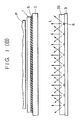
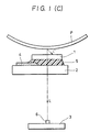
- FIGS. 1(A) and 1(B) schematically show an example of a photoelectric conversion device.
- FIG. 1(A) is a schematic cross-sectional view of the photoelectric conversion device, as seen from the main scanning direction of a photoelectric conversion element array.
- FIG. 1(B) is a schematic cross-sectional view of the device, as seen from the subscanning direction of the photoelectric conversion element array.
- a transparent sensor substrate 1 includes photoelectric conversion elements (not shown) formed on a transparent substrate, made of glass or the like, by a semiconductor process or the like, and an illuminating window (not shown).
- a transparent mounting substrate 2 includes an interconnection wiring member 4 formed on a transparent substrate, made of glass or the like, by a thick-film printing method, a photolithographic method or the like.
- the interconnection member 4 electrically connects the transparent sensor substrate 1 to a driving circuit unit (not shown) provided on the transparent mounting substrate 2.
- the transparent sensor substrate 1 is bonded on the transparent mounting substrate 2 by an adhesive layer 5.
- a light source 3 for emitting light for illuminating an original P comprises an LED array consisting of a plurality of LED chips 6 arranged in the form of an array and a light-condensing member 33 provided thereon.
- the reading position of the original P, the arranged position of the illuminating window in the transparent sensor substrate 1 and the optical axis of the light source 3 in the direction of the array are set to positions which exist within a vertical plane descending from the reading position of the original P, as shown by arrow L.
- Illuminating light L from the light source 3 is projected onto the original P after passing through the transparent mounting substrate 2 and the illuminating window within the transparent sensor substrate 1.
- Information light reflected from the original P is incident upon the photoelectric conversion elements on the transparent sensor substrate 1, and is subjected to photoelectric conversion by the photoelectric conversion elements.
- the converted signal is output to the outside as an image signal.
- FIGS. 1(C) and 1(D) show a modified example of the photoelectric conversion device shown in FIGS. 1(A) and 1(B).
- the modified device differs from the device shown in FIGS. 1(A) and 1(B) only in that there is no light-condensing member 33 provided in the light source 3.
- a linear light source such as a fluoroscent lamp.
- the use of such a light source finds difficulty in providing an inexpensive and small device, since such a light source generally has large external dimensions and is apt to be broken, and the application of an AC voltage, of high voltage and high frequency in some cases, converted from a DC voltage is needed in order to light the light source.
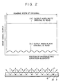
- FIG. 2 shows image signal outputs from the photoelectric conversion device shown in FIG. 1 when a white original and a black original are read.
- an image signal output (a) when a white original is read is nearly uniform over the width of the original, while an image signal output (b) when a black original is read has variations with a large period which corresponds to the arranged pitch of the LED chips. Since the magnitude of the variations in the image signal output when the black original is read is as small as a few % compared with the magnitude of the image signal output when the white original is read, there is practically no problem when the photoelectric conversion device shown in FIG. 1 is used for reading two, i.e., black and white, values.
- This problem which has been found by the inventors of the present invention, is an inherent technical problem which arises when a so-called pseudo-linear light source, in which a plurality of light-emitting sources are arranged in order to provide uniform illuminance on the surface of an original, is combined with a so-called lensless photoelectric conversion device which directly detects light reflected from the original without using a lens array
- the so-called lensless photoelectric conversion device has light source illuminating the original through the transparent substrate including the photoelectric conversion elements. Accordingly, this problem does not arise when a linear light source, such as a fluorescent lamp, is used.
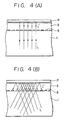
- a white original for example, is illuminated by an LED array, illuminating light beams L are reflected from an original P, and reflected light beams L′ are incident upon photoelectric cnversion elements 8, as shown in FIGS. 3(A) and 3(B). There is also shown a transparent spacer 9.
- the reflected light L′ When the white original is illuminated, the reflected light L′ has a diffused-light component which randomly diffuses with not at all depending on the incident angle of a light beam upon the white original and a specular-reflection-light component which performs specular reflection depending on the incident angle of a light beam.
- FIG. 3(A) shows the behavior of reflected light incident upon photoelectric conversion elements situated just above LED chips.
- FIG. 3(B) shows the behavior of reflected light incident upon photoelectric conversion elements situated at positions above positions between adjacent LED chips.
- both the diffused-light component and the specular-reflection-light component are incident upon the photoelectric conversion elements situated at positions above positions between the LED chips.
- the amount of light beams incident upon photoelectric conversion elements situated just above LED chips becomes smaller by an amount of the specular-reflection-light component.
- the diffused-light component is much larger than the specular-reflection-light component in the component of the light reflected from the surface of the white original, variations in the amount of light beams incident upon the photoelectric conversion elements practically cause no problem.
- the specular-reflection-light component is incident upon photoelectric conversion elements situated at positions above positions between the LED chips.
- a black original is generally prepared by printing black ink on white paper, and it is difficult to prevent the generation of the specular-reflection-light component from the surface of the black ink.
- variations in the amount of light beams incident upon photoelectric conversion elements are further increased.
- It is still another object of the prensent invention to provide a photoelectric conversion device comprising a photosensor comprising a plurality of photoelectric conversion elements and a substrate having a transparent portion for transmitting light for illuminating an original bearing information and provided with the plurality of photoelectric conversion elements, and a light source for emitting light for illuminating the original in which a plurality of light-emitting sources are arranged, the device further comprising light diffusing means between the photosensor and the light source, and to provide an information processing apparatus comprising the photoelectric conversion device, conveying means for conveying the original, and control means for controlling the photoelectric conversion device and the conveying means.
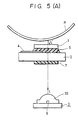
- FIGS. 5(A) and 5(B) are schematic cross-sectional views showing a photoelectric conversion device according to the present invention.
- FIG. 5(A) is a schematic cross-sectional view of the photoelectric conversion device of the present invention, as seen from the main-scanning direction of a photoelectric conversion element array.
- FIG. 5(B) is a schematic cross-sectional view of the device, as seen from the subscanning direction of the photoelectric conversion element array.
- a transparent sensor substrate 1 includes a photoelectric conversion element array formed on a transparent and insulating substrate made of fused quartz, silica glass, borosilicate glass or the like by a semiconductor process or the like.
- a transparent mounting substrate 2 includes an interconnection wiring member 4, made of Ag, Ag-Pd, Ag-Pt, Au or the like formed by a thick-film printing method, or Al, Cu, Mo, ITO (indium-tin oxide) or the like formed by a thin-film forming method and photolithography, provided on a transparent and insulating substrate made of fused quartz, silica glass, borosilicate glass, soda glass, acrylic resin (which may be provided with a protective layer made of SiO2 or the like for preventing elution and diffusion of alkali elements) or the like.
- an interconnection wiring member 4 made of Ag, Ag-Pd, Ag-Pt, Au or the like formed by a thick-film printing method, or Al, Cu, Mo, ITO (indium-tin oxide) or the like formed by a thin-film forming method and photolithography, provided on a transparent and insulating substrate made of fused quartz, silica glass, borosilicate glass, soda glass, acrylic resin (which may
- the interconnection member 4 connects the photoelectric conversion element array to a driving circuit unit (not shown).
- the transparent sensor substrate 1 is bonded on the transparent mounting substrate 2 by an adhesive layer 5.
- a transparent adhesive of a room-temperature-curable, heat-curable or photo-curable type or the like, made of a silicone-type, acryl-type, epoxy-type resin or the like may be suitably used. It is more preferred to use a material having, coefficient of thermal expansion and refractive index which are close to those of each of the transparent sensor substrate 1 and the transparent mounting substrate 2.
- the transparent sensor substrate 1 and the interconnection member 4 of the transparent mounting substrate 2 are electrically connected together using wire bonding, soldering or the like.
- a light source 3 is a pseudo-linear light source comprising an LED array in which a plurality of light-emitting sources consisting of LED chips 6 are linearly arranged.
- a condenser lens 33 serves as a light-condensing member for condensing light in the sub-scanning direction.
- the reading position of the original P, the arranged position of the illuminating window in the transparent sensor substrate 1 and the optical axis of the light source 3 are set to positions which exist within a vertical plane descending from the reading position of the original P.
- any material may be used provided that the material can diffuse illuminating light in the main-scanning direction, that is, in the arranged direction of the LED array.
- a transparent member provided with uneven surface for example the surface having projections and recesses
- Any shape of projections and recesses, either regular or irregular in the main-scanning direction, may be adopted, provided that it achieves the object to diffuse light.
- a member made of an organic material such as polyester, polycarbonate, acrylic resin or the like, or a member made of an inorganic material, such as glass, may be used.
- the shape of the member may also be properly selected according to user's desire.
- the shape of a flexible film, or the shape of a rigid plate may be adopted.
- the projections and recesses may be provided by processing the above-described transparent member by sandblasting or the like, or may be formed using a mold having corresponding projections and recesses.
- a light diffusing means 7 is disposed between the transparent mounting substrate 2 and the light source 3.
- the light diffusing member must be arranged at a position so that the illuminance of the illuminating light from the LED array becomes uniform. If, for example, the light diffusing member is situated very close to the LED array, the effect of the arrangement of the light diffusing member is not sufficiently provided. To the contrary, if the light diffusing member is in close contact with the back of the transparent sensor substrate, an image signal having a high quality can be obtained by sufficiently utilizing the light-diffusing function of the light diffusing member.
- a uniform image signal output can be obtained even when a black original is read.
- a cylindrical lens is usually provided on the LED chips in order to condense light in a direction perpendicular to the array (the subscanning direction) and thus to maintain required illuminance.
- the light diffusing member is situated too close to the LED array, it hinders the effect to condense light by the cylindrical lens, and so there may arise the possibility to reduce the amount of light.
- the light diffusing member close to the photoelectric conversion element array at a position so that the illuminance of the illuminating light becomes uniform, from the viewpoint of providing a high image quality.
- the illuminating light beams L emitted from the light source 3 and having different directional properties according to the positions of the LED arrays become randomly diffused light by the light diffusing plate 7.
- the illuminating light L passes through the transparent mounting substrate 2 and an illuminating window defined by an opaque layer on the transparent sensor substrate 1, and illuminates the original P.
- Information light L′ reflected from the original P is incident upon photoelectric convesion elements 8 on the transparent sensor substrate 1, and is subjected to photoelectric conversion.
- An image signal is output from the photoelectric conversion elements 8.
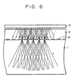
- FIG. 6 shows how information light beams are incident upon the photoelectric conversion elements 8 in the photoelectric conversion device of the present embodiment.
- FIG. 7 shows image signal outputs from the photoelectric conversion device when a white original and a black original are read by the photoelectric conversion device of the present embodiment.
- the illuminating light passing through the light diffusing member has a random directional property at all positions in the main-scanning direction, it is possible to obtain diffused light which does not depend on the arranged positions of the LED chips of the LED array at all.
- the present embodiment there is no difference between the directional property of the light beams of the light illuminating the image surface of the original situated just above the LED chips and the directional property of the light beams of the light illuminating the surface of the original situated at positions above positions between the adjacent LED chips. Hence, it becomes possible to illuminate the original with illuminating light which has a uniform amount of light beams and a random directional property of light beams over the entire reading width of the original.
- a very uniform image signal output can be obtained when a white original is read.
- FIG. 8 is a schematic cross-sectional view showing a configuration in which the photoelectric conversion device of the present invention having the above-described basic configuration is provided as a unit.
- a transparent sensor substrate 1 is bonded on a transparent mounting substrate 2 by an adhesive layer 5, and the transparent mounting substrate 2 is fixed to a base plate 22.
- a diffusing plate 7 has previously been fixed to the base plate 22.
- a light source 3 is then fixed to a lower surface of the base plate 22.
- An image signal can be output from the unit via a flexible interconnection wiring member and a connector (both not illustrated).
- the sensor unit thus configured, it is possible to configure various kinds of information processing apparatuses, such as a facsilime, an image reader and the like.
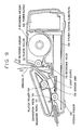
- FIG. 9 illustrates a facsimile as an image information processing apparatus which includes the above-described sensor unit.
- a feeding roller 102 feeds an original P toward a reading position.
- a separation piece 104 securely separates and feeds each sheet of the original P.
- a platen roller 106 provided at the reading position facing the sensor unit 100 regulates the surface to be read of the original P, and also serves as a conveying means for conveying the original P.
- a recording medium PP has the shape of rolled paper in the illustrated example, on which image information read by the photosensor unit or image information transmitted from the outsude in the case of a fascimile or the like is formed.
- a recording head 110 serves as a recording means for performing the above-described image formation.
- a thermal print head, an ink-jet recording head, or various other kinds of heads may be used. Furthermore, the recording head 110 may be of a serial scanning type or a full-line type.
- a platen roller 112 conveys the recording medium PP to a recording position for the recording head 110 and also regulates the surface to be recorded of the recording medium PP.
- An operation panel 120 serving as an input/output means, includes switches for providing operation inputs, display units for indicating messages, states of the apparatus and the like, and other units.
- a system control substrate 130 in which controllers, serving as control means are provided, includes, for example, a control unit for controlling respective units, driving circuitry for the sensor unit, a process unit for image information, a tranceiver unit, and the like.
- a power supply 140 supplies the apparatus and the sensor unit with electric power.
- a photoelectric conversion device comprising a transparent substrate provided with a plurality of photoelectric conversion elements on its surface facing an original from which image information is to be read, and a light source, in which a plurality of light-emitting sources are arranged, provided at the side of the surface of the transparent substrate opposite to the surface facing the original, wherein light emitted from the light source illuminates the original after passing through the substrate and the reflected light is incident upon the photoelectric conversion elements, it is possible to prevent variations in an image signal output when a black original is read and to perform multi-gradation reading by proving a light diffusing member between the photoelectric conversion elements and the light source.
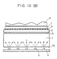
- FIGS. 10(A) and 10(B) A photoelectric conversion device according to the second embodiment of the present invention will be explained by reference to FIGS. 10(A) and 10(B).
- FIG. 10(A) is a schematic cross-sectional view of the device of the second embodiment, as seen from the mainscanning direction of a photoelectric conversion element array.
- FIG. 10(B) is a schematic cross-sectional view of the device of the second embodiment, as seen from the subscanning direction of the photoelectric conversion element array.
- a transparent sensor substrate 1 includes a photoelectric conversion element array formed on a transparent and insulating substrate made of fused quartz, silica glass, borosilicate glass or the like by a semiconductor process or the like.
- a transparent mounting substrate 2 includes an interconnection wiring member 4, made of Ag, Ag-Pd, Ag-Pt, Au or the like formed by a thick-film printing method, or Al, Cu, Mo, ITO (indium-tin oxide) or the like formed by a thin-film forming method and photolithography, provided on a transparent and insulating substrate made of fused quartz, silica glass, borosilicate glass, soda glass, acrylic resin (which may be provided with a protective layer made of SiO2 or the like for preventing elution and diffusion of alkali elements) or the like.
- an interconnection wiring member 4 made of Ag, Ag-Pd, Ag-Pt, Au or the like formed by a thick-film printing method, or Al, Cu, Mo, ITO (indium-tin oxide) or the like formed by a thin-film forming method and photolithography, provided on a transparent and insulating substrate made of fused quartz, silica glass, borosilicate glass, soda glass, acrylic resin (which may
- the interconnection member 4 connects the photoelectric conversion element array to a driving circuit unit (not shown).
- the transparent sensor substrate 1 is bonded on the transparent mounting substrate 2 by an adhesive layer 5.
- a transparent adhesive of a room-temperature-curable, heat-curable or photo-curable type or the like, made of a silicone-type, acryl-type, epoxy-type resin or the like may be suitably used.
- a material having coefficient of thermal expansion and refractive index which are close to those of each of the transparent sensor substrate 1 and the transparent mounting substrate 2 is used.
- the transparent sensor substrate 1 and the interconnection member 4 on the transport mounting substrate 2 are electrically connected together using wire bonding, soldering or the like.
- a light source 3 is a pseudo-linear light source comprising an LED array in which a plurality of light-emitting sources consisting of LED chips 6 are linearly arranged.
- the reading position of the original P, the arranged position of an illuminating window (not shown) in the transparent sensor substrate 1 and the optical axis of the light source 3 are set to positions which exist within a vertical plane descending from the reading position of the original P.
- a pseudo-linear light source such as an LED array or the like
- directional properties of illuminating light beams are different between positions just above light-emitting sources such as LED chips and positions above positions between adjacent light-emitting sources.
- the light-guiding means 7 has a length which nearly corresponds to the length of the light source 3 and the photoelectric conversion element array in the main-scanning direction, has the shape of a rectangular cross section longer in the main-scanning direction, and is made of a material, such as acrylic resin or the like.
- a large number of fine grooves extending in a direction nearly perpendicular to the direction of arrangement of the LED chips 6 are regularly formed as light scattering means.
- Illuminating light L emitted from the light source 3 enters from an incident surface 7a, facing the light surce 3, of the light-guiding means 7 into the light-guiding means 7.
- a part of the entered light L proceeds within the light-guiding means 7 while performing total reflection at side 7b of the light-guiding means 7, and reaches the exit surface 7c on which the fine grooves are formed. Since the large number of fine grooves are regularly formed on the exit surface 7c, the light beams of the illuminating light L are diffused in the direction of arrangement of the LED chips 6, in other words, in the main-scanning direction of the photoelectric conversion element array, by the grooves. At this time, the light beams are hardly diffused in a direction perpendicular to the direction of arrangement of the LED chips 6, in other words, in the subscanning direction of the photoelectric conversion element array.
- the diffused light beams then pass through the transparent mounting substrate 2 and the transparent sensor substrate 1, and illuminate the original P.
- Information light L′ reflected from the original P is incident upon the photoelectric conversion elements on the transparent sensor substrate 1, and an image signal is output from the photoelectric conversion elements.
- the photoelectric conversion device of the present embodiment having the above-described configuration has the following effects:
- illuminating light L has a random diffusing property and a nearly uniform illuminance.
- a diffused-light component and a specular-reflection-light component are produced as the components of the light L′ reflected from the surface of the white original, the component of the reflected light L′ incident upon each photoelectric conversion element 14 becomes uniform.
- a uniform and large output signal (larger photo-curent) can be obtained from the photoelectric conversion elements 14.
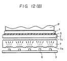
- FIGS. 12(A) and 12(B), showing a third embodiment of the present invention are cross-sectional views schematically showing a photoelectric conversion device of the embodiment.
- FIG. 12(A) is a schematic cross-sectional view of the device as seen from the main-scanning direction of a photoelectric conversion element array.
- FIG. 12(B) is a schematic cross-sectional view of the device as seen from the subscanning direction of the array.
- the third embodiment differs from the second embodiment in that the length of the light-guiding means 7 in the direction of the optical axis is smaller, and a large number of grooves, serving as light-scattering means, extending in a direction nearly perpendicular to the direction of arrangement of the LED chips 6 are partially provided also on the incident surface 7a of the light-guiding means 7.
- the length of the light-guiding means 7 in the direction of the optical axis as small as possible.
- the length of the light-guiduing means 7 is merely shortened in the structure of the second embodiment, there is the possibility of the occurrence of unevenness in illuminance and in the directional property of light beams.
- a certain amount of length is needed.
- Furthermore if a uniform illuminance cannot be obtained at the exit surface 7c of the light-guiding member 7, diffused light may not be obtained in some cases even if grooves are provided on the exit surface 7c.
- the third embodiment by providing the large number of grooves extending in a direction nearly perpendicular to the direction of arrangement of the LED chips 6 on portions above the LED chips on the incident surface 7a of the light-guiding surface 7a, illuminating light emitted from the LED chips 6 is diffused in the main-scanning direction at the incident surface 7a of the light-guiding member 7.
- the illuminating light diffused at the incident surface 7a proceeds while performing total reflection within the light-guiding member 7. Where a uniform illuminance is obtained, the illuminating light is diffused again in the main-scanning direction by the grooves provided on the exit surface 7c.
- the shape of the grooves is not limited thereto. Any shape capable of realizing the technical concept of the present invention may be adopted.
- the shape of a sine-curve may, for example, be adopted. In this case, however, it is desirable that the length of one period be as fine as the above-described grooves.
- the partial arrangement of the grooves on the incident surface of the light-guiding means depends on the arranged position of the plurality of light-emitting sources, directivity of the emission, and the like. Accordingly, the grooves may be formed not, only on positions near just above the light-emitting sources, as in the third embodiment, but also on other positions.
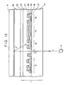
- FIG. 13 is a schematic cross-sectional view of a transparent sensor substrate, serving as a photosensing unit, according to the present embodiment, as seen from the main-scanning direction of a photoelectric conversion element array.
- a transparent glass substrate 11 On a transparent glass substrate 11 are formed a matrix interconnection wiring member 12 by thin-film forming method, an illuminating window 13, photoelectric conversion elements 14, charge storage members 15 and thin-film transistors (TFTs) 16 for transferring stored electric charges with a proper timing.
- TFTs thin-film transistors
- Each of these elements is formed by an identical production process by sequentially stacking layers of a light-tight lower electrode 17 made of Cr, an insulating layer 18 made of SiN, a photoconductive layer 19 made of a-Si:H as non-single crystalline Si, an ohmic-contact layer 20 made of n+-type a-Si:H and an upper electrode 21 made of Al on the glass substrate 11.
- the photoelectric conversion elements 14, the charge storage members 15, the TFTs 16 and the like are coated with a passivation layer 22 made of SiN, on which a protective layer 24 made of a thin glass plate is provided via an adhesive layer 23 made of epoxy resin.
- the thin glass plate 24 has the function as an anti-friction layer for protecting the photoelectric conversion elements 14 and the like from friction with the original P, and the function as a spacer for maintaining the distance between the original P and the photoelectric conversion elements 14 constant.
- illuminating light L emitted from a light source 4 provided at the side of the surface of the transparent sensor substrate 1 opposite to the original P illuminates the original P after passing through the transparent sensor substrate 1.
- Information light L′ reflected from the original P is incident upon the photoelectric conversion elements 14.
- the photoelectric conversion devices according to the second and third embodiments may be applied to the image information processing apparatus (for example, a facsimile) shown in FIG. 9 or the like.
- a photoelectric conversion device comprising a substrate provided with a plurality of photoelectric conversion elements on the surface facing an original from which image information is to be read and a light source in which a plurality of light-emitting sources are arranged, wherein light emitted from the light source illuminates the original and light reflected there from is incident upon the photoelectric conversion elements, by providing a light-guiding means between the photoelectric conversion elements and the light source, and by providing a large number of grooves extending in a direction crossing, more preferably, substantially perpendiculer to the direction of arrangement of the light source on at least one of an incident surface and an exit surface of the light-guiding means, as optical-axis changing means for the illuminating light, it is possible to realize an inexpensive and small photoelectric conversion device while making illuminance on the original large and uniform.
- a photoelectric conversion device includes a photosensor including a plurality of photoelectric conversion elements and a substrate having a transparent portion for transmitting light for illuminating an original bearing information and provided with the plurality of photoelectric conversion elements, and a light source for emitting light for illuminating the original in which a plurality of light-emitting sources are arranged.
- the device further includes a light diffuser between the photosensor and the light source.
Abstract
Description
- This invention relates to a photoelectric conversion device, and more particularly, to a photoelectric conversion device used as an input unit for a facsimile, an image reader, a digital copying machine, an electronic blackboard or the like.
- Recently, long line sensors having optical systems with one-to-one magnification ratio have been developed as photoelectric conversion devices for the purpose of providing small and high-performance facsimiles, image readers, and the like.
- Furthermore, for the purpose of providing small and inexpensive devices, photoelectric conversion devices have also been proposed in which a sensor directly detects light reflected from an original via a transparent spacer made of glass or the like without using a fiber lens array with one- to-one magnification ratio.
- FIGS. 1(A) and 1(B) schematically show an example of a photoelectric conversion device. FIG. 1(A) is a schematic cross-sectional view of the photoelectric conversion device, as seen from the main scanning direction of a photoelectric conversion element array. FIG. 1(B) is a schematic cross-sectional view of the device, as seen from the subscanning direction of the photoelectric conversion element array.
- In FIGS. 1(A) and 1(B), a
transparent sensor substrate 1 includes photoelectric conversion elements (not shown) formed on a transparent substrate, made of glass or the like, by a semiconductor process or the like, and an illuminating window (not shown). Atransparent mounting substrate 2 includes aninterconnection wiring member 4 formed on a transparent substrate, made of glass or the like, by a thick-film printing method, a photolithographic method or the like. Theinterconnection member 4 electrically connects thetransparent sensor substrate 1 to a driving circuit unit (not shown) provided on thetransparent mounting substrate 2. Thetransparent sensor substrate 1 is bonded on thetransparent mounting substrate 2 by anadhesive layer 5. Alight source 3 for emitting light for illuminating an original P comprises an LED array consisting of a plurality ofLED chips 6 arranged in the form of an array and a light-condensingmember 33 provided thereon. - The reading position of the original P, the arranged position of the illuminating window in the
transparent sensor substrate 1 and the optical axis of thelight source 3 in the direction of the array are set to positions which exist within a vertical plane descending from the reading position of the original P, as shown by arrow L. - Illuminating light L from the
light source 3 is projected onto the original P after passing through thetransparent mounting substrate 2 and the illuminating window within thetransparent sensor substrate 1. Information light reflected from the original P is incident upon the photoelectric conversion elements on thetransparent sensor substrate 1, and is subjected to photoelectric conversion by the photoelectric conversion elements. The converted signal is output to the outside as an image signal. - FIGS. 1(C) and 1(D) show a modified example of the photoelectric conversion device shown in FIGS. 1(A) and 1(B). The modified device differs from the device shown in FIGS. 1(A) and 1(B) only in that there is no light-condensing
member 33 provided in thelight source 3. - However, in attempts to provide a further inexpensive and smaller device, it has become clear that the above-described photoelectric conversion devices have the following technical problems.
- As a means for providing an inexpensive photoelectric conversion device, it is possible to reduce the number of the LED chips and thus to reduce the cost of the light source.
- When the number of the LED chips are reduced, illuminance on the surface of the original is reduced, causing uneven illuminance. This substantially deteriorates the quality of an image, especially when a white original is read.
- In order to reduce the uneven illuminance, it is possible to increase the distance between the LED array and the surface of the original. This approach, however, is by no means preferable, since the illuminance substantially decreases and the photoelectric conversion device becomes large.
- On the other hand, when an original is illuminated by the LED array, much light beams nearly perpendicular to the surface of the original are incident upon the surface of the original situated just above the LED chips, but much light beams inclined relative to the surface of the original are incident upon the surface of the original situated at positions above positions between the LED chips. That is, when an original is illuminated by a so-called pseuodo-linear light source in which a plurality of light-emitting sources are arranged, a directional property which the light beams of the illuminating light have causes uneven directional property of the light beam within the area of the surface of the original. If the illuminating light has such a directional unevenness, the quality of an image is substantially deteriorated when a black original is read.
- In order to prevent the directional unevenness in the illuminating light, it is possible to use a linear light source, such as a fluoroscent lamp. The use of such a light source, however, finds difficulty in providing an inexpensive and small device, since such a light source generally has large external dimensions and is apt to be broken, and the application of an AC voltage, of high voltage and high frequency in some cases, converted from a DC voltage is needed in order to light the light source.
- The above-described technical problems will now be explained in detail.
- FIG. 2 shows image signal outputs from the photoelectric conversion device shown in FIG. 1 when a white original and a black original are read.
- According to FIG. 2, it can be understood that an image signal output (a) when a white original is read is nearly uniform over the width of the original, while an image signal output (b) when a black original is read has variations with a large period which corresponds to the arranged pitch of the LED chips. Since the magnitude of the variations in the image signal output when the black original is read is as small as a few % compared with the magnitude of the image signal output when the white original is read, there is practically no problem when the photoelectric conversion device shown in FIG. 1 is used for reading two, i.e., black and white, values.
- When the device is used for reading multiple gradations, however, although the magnitude of variations in an image output when a black original is read is small, a noise corresponding to the arranged pitch of the LED chips appears as stripes in a reproduced output image corresponding to the black original in some setting of slice levels for providing the color density of the image of the original with multiple values. This deteriorates the picture quality.
- This problem, which has been found by the inventors of the present invention, is an inherent technical problem which arises when a so-called pseudo-linear light source, in which a plurality of light-emitting sources are arranged in order to provide uniform illuminance on the surface of an original, is combined with a so-called lensless photoelectric conversion device which directly detects light reflected from the original without using a lens array In other words, the so-called lensless photoelectric conversion device has light source illuminating the original through the transparent substrate including the photoelectric conversion elements. Accordingly, this problem does not arise when a linear light source, such as a fluorescent lamp, is used.
- Before explaining embodiments according to the present invention, the above-described problem will be explained by reference to the accompanying drawings.
- Even in a pseudo-linear light source such as an LED array or the like, the amounts of light beams illuminating the surface of an original are nearly identical at a position just above an LED chip and at a position above a position between adjacent LED chips.
- When a white original, for example, is illuminated by an LED array, illuminating light beams L are reflected from an original P, and reflected light beams L′ are incident upon
photoelectric cnversion elements 8, as shown in FIGS. 3(A) and 3(B). There is also shown atransparent spacer 9. - When the white original is illuminated, the reflected light L′ has a diffused-light component which randomly diffuses with not at all depending on the incident angle of a light beam upon the white original and a specular-reflection-light component which performs specular reflection depending on the incident angle of a light beam.
- FIG. 3(A) shows the behavior of reflected light incident upon photoelectric conversion elements situated just above LED chips.
- As shown in FIG. 3(A), very few specular-reflection light component is included within the compoment of the reflected light incident upon the photoelectric conversion elements situated just above the LED chips. Since the illuminating light L passes through the illuminating window in the
transparent sensor substrate 1 and illuminates the original P with an angle almost perpendicular to the original P, the specular-reflection-light component L′ passes again through the illuminating window and goes to the outside. - FIG. 3(B) shows the behavior of reflected light incident upon photoelectric conversion elements situated at positions above positions between adjacent LED chips.
- As shown in FIG. 3(B), both the diffused-light component and the specular-reflection-light component are incident upon the photoelectric conversion elements situated at positions above positions between the LED chips.
- Accordingly, if a white original is illuminated by a pseudo-linear light source, the amount of light beams incident upon photoelectric conversion elements situated just above LED chips becomes smaller by an amount of the specular-reflection-light component. However, since the diffused-light component is much larger than the specular-reflection-light component in the component of the light reflected from the surface of the white original, variations in the amount of light beams incident upon the photoelectric conversion elements practically cause no problem.
- On the other hand, when, a black original is illumunated by a pseudo-linear light source, since illuminating light beams are absorbed on the surface of the original and are hardly diffused, as shown in FIGS. 4(A) and 4(B), the specular-reflection-light component is emphasized.
- As shown in FIG. 4(A), since the illuminating light is absorbed by the black original, the diffused light and the specular-reflection-light component L′ reflected are hardly incident upon photoelectric conversion elements situated just above LED chips.
- To the contrary, as shown in FIG. 4(B), the specular-reflection-light component is incident upon photoelectric conversion elements situated at positions above positions between the LED chips. This is because a black original is generally prepared by printing black ink on white paper, and it is difficult to prevent the generation of the specular-reflection-light component from the surface of the black ink. Thus, when a black original is read, variations in the amount of light beams incident upon photoelectric conversion elements are further increased.
- It is an object of the present invention to provide a photoelectric conversion device and an information processing apparatus which are less expensive, more compact and have higher performance than ever.
- It is a further object of the present invention to provide a photoelectric conversion device and an information processing apparatus in which excellent linear illuminating light can be obtained even if the number of light-emitting sources is decreased.
- It is a still further object of the prensent invention to provide a photoelectric conversion device and an information processing apparatus having improved illuminating systems in which subtantially uniform information light can be obtained for any original to be read.
- It is still another object of the prensent invention to provide a photoelectric conversion device comprising a photosensor comprising a plurality of photoelectric conversion elements and a substrate having a transparent portion for transmitting light for illuminating an original bearing information and provided with the plurality of photoelectric conversion elements, and a light source for emitting light for illuminating the original in which a plurality of light-emitting sources are arranged, the device further comprising light diffusing means between the photosensor and the light source, and to provide an information processing apparatus comprising the photoelectric conversion device, conveying means for conveying the original, and control means for controlling the photoelectric conversion device and the conveying means.
-
- FIGS. 1(A) and 1(B) are schematic cross-sectional views showing an example of a photoelectric conversion device;
- FIGS. 1(C) and 1(D) are schematic cross-sectional views showing another example of a photoelectric conversion device;
- FIG. 2 is a graph for explaining image signal outputs;
- FIGS. 3(A) and 3(B) are schematic diagrams for explaining illuminating light;
- FIGS. 4(A) and 4(B) are schematic diagrams also for explaining illuminating light;
- FIGS. 5(A) and 5(B) are schematic cross-sectional views of a photoelectric conversion device according to the present invention;
- FIG. 6 is a schematic diagram for explaining illuminating light in the photoelectric conversion device according to the present invention;
- FIG. 7 is a graph for explaining image signal outputs according to the present invention;
- FIG. 8 is a schematic cross-sectional view of a photoelectric conversion device unit according to the present invention;
- FIG. 9 is a schematic cross-sectional view of an information processing apparatus according to the present invention;
- FIGS. 10(A) and 10(B) are schematic cross-sectional views of another photoelectric conversion device according to the present invention;
- FIGS. 11(A) and 11(B) are schematic diagrams for explaining illuminating light in the photoelectric conversion device according to the present invention;
- FIGS. 12(A) and 12(B) are schematic cross-sectional views of still another photoelectric conversion device according to the present invention; and
- FIGS. 13(A) and 13(B) are schematic cross-sectional views showing a photosensor unit which is suitable for a photoelectric conversion device according to the present invention.
- The present invention will now be explained in detail by reference to the drawings.
- FIGS. 5(A) and 5(B) are schematic cross-sectional views showing a photoelectric conversion device according to the present invention. FIG. 5(A) is a schematic cross-sectional view of the photoelectric conversion device of the present invention, as seen from the main-scanning direction of a photoelectric conversion element array. FIG. 5(B) is a schematic cross-sectional view of the device, as seen from the subscanning direction of the photoelectric conversion element array.
- In FIGS. 1(A) and 1(B), a
transparent sensor substrate 1 includes a photoelectric conversion element array formed on a transparent and insulating substrate made of fused quartz, silica glass, borosilicate glass or the like by a semiconductor process or the like. - A
transparent mounting substrate 2 includes aninterconnection wiring member 4, made of Ag, Ag-Pd, Ag-Pt, Au or the like formed by a thick-film printing method, or Al, Cu, Mo, ITO (indium-tin oxide) or the like formed by a thin-film forming method and photolithography, provided on a transparent and insulating substrate made of fused quartz, silica glass, borosilicate glass, soda glass, acrylic resin (which may be provided with a protective layer made of SiO₂ or the like for preventing elution and diffusion of alkali elements) or the like. - The
interconnection member 4 connects the photoelectric conversion element array to a driving circuit unit (not shown). Thetransparent sensor substrate 1 is bonded on thetransparent mounting substrate 2 by anadhesive layer 5. For theadhesive layer 5, a transparent adhesive of a room-temperature-curable, heat-curable or photo-curable type or the like, made of a silicone-type, acryl-type, epoxy-type resin or the like may be suitably used. It is more preferred to use a material having, coefficient of thermal expansion and refractive index which are close to those of each of thetransparent sensor substrate 1 and thetransparent mounting substrate 2. Thetransparent sensor substrate 1 and theinterconnection member 4 of thetransparent mounting substrate 2 are electrically connected together using wire bonding, soldering or the like. - A
light source 3 is a pseudo-linear light source comprising an LED array in which a plurality of light-emitting sources consisting ofLED chips 6 are linearly arranged. Acondenser lens 33 serves as a light-condensing member for condensing light in the sub-scanning direction. - The reading position of the original P, the arranged position of the illuminating window in the
transparent sensor substrate 1 and the optical axis of thelight source 3 are set to positions which exist within a vertical plane descending from the reading position of the original P. - As described above, although, in a pseudo-linear light source such as an LED array or the like, directional properties of illuminating light beams are different between positions just above light-emitting sources such as LED chips and positions above positions between adjacent light-emitting sources, the problems thereby caused are solved by providing a light diffusing means.
- For the light diffusing means, any material may be used provided that the material can diffuse illuminating light in the main-scanning direction, that is, in the arranged direction of the LED array.
- More specifically, it is preferred to use a transparent member provided with uneven surface (for example the surface having projections and recesses), because it can be easily made and so coincides with the basic technical conception of low cost.
- Any shape of projections and recesses, either regular or irregular in the main-scanning direction, may be adopted, provided that it achieves the object to diffuse light.
- For example, a member made of an organic material, such as polyester, polycarbonate, acrylic resin or the like, or a member made of an inorganic material, such as glass, may be used.
- The shape of the member may also be properly selected according to user's desire. For example, the shape of a flexible film, or the shape of a rigid plate may be adopted.
- The projections and recesses may be provided by processing the above-described transparent member by sandblasting or the like, or may be formed using a mold having corresponding projections and recesses.
- It is preferred to provide such a light diffusing means between the photoelectric conversion element array and the light source. In the FIG. 5 example, a light diffusing means 7 is disposed between the
transparent mounting substrate 2 and thelight source 3. - In order to obtain a high image quality by sufficiently utilizing the light-diffusing function of the light diffusing member, it is necessary to devise the arrangement of the light-diffusing member.
- The light diffusing member must be arranged at a position so that the illuminance of the illuminating light from the LED array becomes uniform. If, for example, the light diffusing member is situated very close to the LED array, the effect of the arrangement of the light diffusing member is not sufficiently provided. To the contrary, if the light diffusing member is in close contact with the back of the transparent sensor substrate, an image signal having a high quality can be obtained by sufficiently utilizing the light-diffusing function of the light diffusing member.
- Thus, according to the photoelectric conversion device according to the present embodiment, a uniform image signal output can be obtained even when a black original is read.
- In the LED array, a cylindrical lens is usually provided on the LED chips in order to condense light in a direction perpendicular to the array (the subscanning direction) and thus to maintain required illuminance. Hence, if the light diffusing member is situated too close to the LED array, it hinders the effect to condense light by the cylindrical lens, and so there may arise the possibility to reduce the amount of light.
- Accordingly, in the photoelectric conversion device of the present invention, it is preferred to dispose the light diffusing member close to the photoelectric conversion element array at a position so that the illuminance of the illuminating light becomes uniform, from the viewpoint of providing a high image quality.
- The illuminating light beams L emitted from the
light source 3 and having different directional properties according to the positions of the LED arrays become randomly diffused light by thelight diffusing plate 7. - Subsequently, the illuminating light L passes through the
transparent mounting substrate 2 and an illuminating window defined by an opaque layer on thetransparent sensor substrate 1, and illuminates the original P. Information light L′ reflected from the original P is incident uponphotoelectric convesion elements 8 on thetransparent sensor substrate 1, and is subjected to photoelectric conversion. An image signal is output from thephotoelectric conversion elements 8. - FIG. 6 shows how information light beams are incident upon the
photoelectric conversion elements 8 in the photoelectric conversion device of the present embodiment. - FIG. 7 shows image signal outputs from the photoelectric conversion device when a white original and a black original are read by the photoelectric conversion device of the present embodiment.
- As described above, since the illuminating light passing through the light diffusing member has a random directional property at all positions in the main-scanning direction, it is possible to obtain diffused light which does not depend on the arranged positions of the LED chips of the LED array at all.
- That is, according to the present embodiment, there is no difference between the directional property of the light beams of the light illuminating the image surface of the original situated just above the LED chips and the directional property of the light beams of the light illuminating the surface of the original situated at positions above positions between the adjacent LED chips. Hence, it becomes possible to illuminate the original with illuminating light which has a uniform amount of light beams and a random directional property of light beams over the entire reading width of the original.
- Accordingly, although, when a white original is read, a diffused-light component and a specular-reflection-light component are produced as the components of the light reflected from the surface of the white original, there appear no variations in the components of reflected light incident upon the photoelectric conversion elements since the illuminating light which was diffused by the light diffusing means has a uniform amount of light beams and a random diffusing property.
- Thus, according to the photoelectric conversion device according to the present embodiment, a very uniform image signal output can be obtained when a white original is read.
- Furthermore, although, when a black original is read, only the specular-reflection-light component is emphasized as the component of the light reflected from the surface of the black original, there appear no variations in the components of reflected light incident upon the photoelectric conversion elements since the illuminating light which was diffused by the light diffusing means has a uniform amount of light beams and a random directional property.
- FIG. 8 is a schematic cross-sectional view showing a configuration in which the photoelectric conversion device of the present invention having the above-described basic configuration is provided as a unit. In the illustrated ex ample, a
transparent sensor substrate 1 is bonded on atransparent mounting substrate 2 by anadhesive layer 5, and thetransparent mounting substrate 2 is fixed to abase plate 22. A diffusingplate 7 has previously been fixed to thebase plate 22. Alight source 3 is then fixed to a lower surface of thebase plate 22. An image signal can be output from the unit via a flexible interconnection wiring member and a connector (both not illustrated). - Using the sensor unit thus configured, it is possible to configure various kinds of information processing apparatuses, such as a facsilime, an image reader and the like.
- FIG. 9 illustrates a facsimile as an image information processing apparatus which includes the above-described sensor unit. In FIG. 9, a feeding
roller 102 feeds an original P toward a reading position. A separation piece 104 securely separates and feeds each sheet of the original P. Aplaten roller 106 provided at the reading position facing thesensor unit 100 regulates the surface to be read of the original P, and also serves as a conveying means for conveying the original P. - A recording medium PP has the shape of rolled paper in the illustrated example, on which image information read by the photosensor unit or image information transmitted from the outsude in the case of a fascimile or the like is formed. A
recording head 110 serves as a recording means for performing the above-described image formation. As therecording head 110, a thermal print head, an ink-jet recording head, or various other kinds of heads may be used. Furthermore, therecording head 110 may be of a serial scanning type or a full-line type. Aplaten roller 112 conveys the recording medium PP to a recording position for therecording head 110 and also regulates the surface to be recorded of the recording medium PP. - An operation panel 120, serving as an input/output means, includes switches for providing operation inputs, display units for indicating messages, states of the apparatus and the like, and other units.
- A
system control substrate 130, in which controllers, serving as control means are provided, includes, for example, a control unit for controlling respective units, driving circuitry for the sensor unit, a process unit for image information, a tranceiver unit, and the like. Apower supply 140 supplies the apparatus and the sensor unit with electric power. - As explained above, according the present embodiment, in a photoelectric conversion device comprising a transparent substrate provided with a plurality of photoelectric conversion elements on its surface facing an original from which image information is to be read, and a light source, in which a plurality of light-emitting sources are arranged, provided at the side of the surface of the transparent substrate opposite to the surface facing the original, wherein light emitted from the light source illuminates the original after passing through the substrate and the reflected light is incident upon the photoelectric conversion elements, it is possible to prevent variations in an image signal output when a black original is read and to perform multi-gradation reading by proving a light diffusing member between the photoelectric conversion elements and the light source.
- A second embodiment of the present invention will now be explained in detail with reference to the drawings.
- A photoelectric conversion device according to the second embodiment of the present invention will be explained by reference to FIGS. 10(A) and 10(B).
- FIG. 10(A) is a schematic cross-sectional view of the device of the second embodiment, as seen from the mainscanning direction of a photoelectric conversion element array. FIG. 10(B) is a schematic cross-sectional view of the device of the second embodiment, as seen from the subscanning direction of the photoelectric conversion element array.
- In FIGS. 10(A) and 10(B), a
transparent sensor substrate 1 includes a photoelectric conversion element array formed on a transparent and insulating substrate made of fused quartz, silica glass, borosilicate glass or the like by a semiconductor process or the like. - A
transparent mounting substrate 2 includes aninterconnection wiring member 4, made of Ag, Ag-Pd, Ag-Pt, Au or the like formed by a thick-film printing method, or Al, Cu, Mo, ITO (indium-tin oxide) or the like formed by a thin-film forming method and photolithography, provided on a transparent and insulating substrate made of fused quartz, silica glass, borosilicate glass, soda glass, acrylic resin (which may be provided with a protective layer made of SiO₂ or the like for preventing elution and diffusion of alkali elements) or the like. - The
interconnection member 4 connects the photoelectric conversion element array to a driving circuit unit (not shown). Thetransparent sensor substrate 1 is bonded on thetransparent mounting substrate 2 by anadhesive layer 5. For theadhesive layer 5, a transparent adhesive of a room-temperature-curable, heat-curable or photo-curable type or the like, made of a silicone-type, acryl-type, epoxy-type resin or the like may be suitably used. A material having coefficient of thermal expansion and refractive index which are close to those of each of thetransparent sensor substrate 1 and thetransparent mounting substrate 2 is used. Thetransparent sensor substrate 1 and theinterconnection member 4 on thetransport mounting substrate 2 are electrically connected together using wire bonding, soldering or the like. - A
light source 3 is a pseudo-linear light source comprising an LED array in which a plurality of light-emitting sources consisting ofLED chips 6 are linearly arranged. - The reading position of the original P, the arranged position of an illuminating window (not shown) in the
transparent sensor substrate 1 and the optical axis of thelight source 3 are set to positions which exist within a vertical plane descending from the reading position of the original P. - As described above, in a pseudo-linear light source such as an LED array or the like, directional properties of illuminating light beams are different between positions just above light-emitting sources such as LED chips and positions above positions between adjacent light-emitting sources.
- A light-guiding means 7, disposed between the photoelectric conversion element array on the
transparent sensor substrate 1 and thelight source 3, efficiently and uniformly guides illuminating light L emitted from thelight source 3 to the surface of the original while reducing unevenness in illuminating light beams. - The light-guiding means 7 has a length which nearly corresponds to the length of the
light source 3 and the photoelectric conversion element array in the main-scanning direction, has the shape of a rectangular cross section longer in the main-scanning direction, and is made of a material, such as acrylic resin or the like. On anexit surface 7c of the light-guiding means 7, a large number of fine grooves extending in a direction nearly perpendicular to the direction of arrangement of theLED chips 6 are regularly formed as light scattering means. - Illuminating light L emitted from the
light source 3 enters from anincident surface 7a, facing thelight surce 3, of the light-guiding means 7 into the light-guidingmeans 7. A part of the entered light L proceeds within the light-guiding means 7 while performing total reflection atside 7b of the light-guiding means 7, and reaches theexit surface 7c on which the fine grooves are formed. Since the large number of fine grooves are regularly formed on theexit surface 7c, the light beams of the illuminating light L are diffused in the direction of arrangement of theLED chips 6, in other words, in the main-scanning direction of the photoelectric conversion element array, by the grooves. At this time, the light beams are hardly diffused in a direction perpendicular to the direction of arrangement of theLED chips 6, in other words, in the subscanning direction of the photoelectric conversion element array. - The diffused light beams then pass through the
transparent mounting substrate 2 and thetransparent sensor substrate 1, and illuminate the original P. Information light L′ reflected from the original P is incident upon the photoelectric conversion elements on thetransparent sensor substrate 1, and an image signal is output from the photoelectric conversion elements. - The photoelectric conversion device of the present embodiment having the above-described configuration has the following effects:
- (1) Since the illuminating light proceeds within the light-guiding means while repeating total reflection, illuminance is not decreased, and unevenness in illuminance can also be reduced.
- (2) Since the light beams of the illuminating light are diffused in the main-scanning direction by the fine grooves at the exit surface of the light-guiding means, unevenness is not produced in the directional property of the light beams.
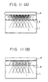
- The effects of the photoelectric conversion device of the present embodiment will be explained by reference to FIGS. 11(A) and 11(B).
- As shown in FIG. 11(A), when a white original P is read by the photoelectric conversion device of the present embodiment, illuminating light L has a random diffusing property and a nearly uniform illuminance. Hence, although a diffused-light component and a specular-reflection-light component are produced as the components of the light L′ reflected from the surface of the white original, the component of the reflected light L′ incident upon each
photoelectric conversion element 14 becomes uniform. Accordingly, a uniform and large output signal (larger photo-curent) can be obtained from thephotoelectric conversion elements 14. - As shown in FIG. 11(B), when a black original is read by the photoelectric conversion device of the present embodiment, only a very small amount of a specular-reflection component which is reflected without being absorbed on the surface of the original is produced as the component of the light L′ reflected from the surface of the black original. However, since the illuminating light L has a random diffusing property and a nearly uniform illuminance, the component of the reflected light L′ incident upon each
photoelectric conversion element 14 is uniform. Accordingly, a uniform and small output signal (smaller dark-current) can be obtained from thephotoelectric conversion elements 14. - FIGS. 12(A) and 12(B), showing a third embodiment of the present invention, are cross-sectional views schematically showing a photoelectric conversion device of the embodiment. FIG. 12(A) is a schematic cross-sectional view of the device as seen from the main-scanning direction of a photoelectric conversion element array. FIG. 12(B) is a schematic cross-sectional view of the device as seen from the subscanning direction of the array.
- The third embodiment differs from the second embodiment in that the length of the light-guiding means 7 in the direction of the optical axis is smaller, and a large number of grooves, serving as light-scattering means, extending in a direction nearly perpendicular to the direction of arrangement of the
LED chips 6 are partially provided also on theincident surface 7a of the light-guidingmeans 7. - In order to provide a small photoelectric conversion device, it is desired to make the length of the light-guiding means 7 in the direction of the optical axis as small as possible. However, if the length of the light-guiduing means 7 is merely shortened in the structure of the second embodiment, there is the possibility of the occurrence of unevenness in illuminance and in the directional property of light beams. In order to obtain a uniform illuminance by repeating total reflection within the light-guiding
member 7, a certain amount of length is needed. Furthermore, if a uniform illuminance cannot be obtained at theexit surface 7c of the light-guidingmember 7, diffused light may not be obtained in some cases even if grooves are provided on theexit surface 7c. - In the third embodiment, by providing the large number of grooves extending in a direction nearly perpendicular to the direction of arrangement of the
LED chips 6 on portions above the LED chips on theincident surface 7a of the light-guidingsurface 7a, illuminating light emitted from theLED chips 6 is diffused in the main-scanning direction at theincident surface 7a of the light-guidingmember 7. The illuminating light diffused at theincident surface 7a proceeds while performing total reflection within the light-guidingmember 7. Where a uniform illuminance is obtained, the illuminating light is diffused again in the main-scanning direction by the grooves provided on theexit surface 7c. - Accordingly, even if the length of the light-guiding
member 7 in the direction of the optical axis is small, illuminance on the surface of the original is uniform, and unevenness in the directional property of the light beams is not produced. - Although, in the second and third embodiments, the large number of grooves provided on the incident surface and the exit surface of the light-guiding means have the shape of triangular cross-sections, the shape of the grooves is not limited thereto. Any shape capable of realizing the technical concept of the present invention may be adopted. The shape of a sine-curve may, for example, be adopted. In this case, however, it is desirable that the length of one period be as fine as the above-described grooves.
- The partial arrangement of the grooves on the incident surface of the light-guiding means depends on the arranged position of the plurality of light-emitting sources, directivity of the emission, and the like. Accordingly, the grooves may be formed not, only on positions near just above the light-emitting sources, as in the third embodiment, but also on other positions.
- The present invention is of course not limited to the above-described embodiments, but various changes and modifications may be made within the scope of the invention.
- FIG. 13 is a schematic cross-sectional view of a transparent sensor substrate, serving as a photosensing unit, according to the present embodiment, as seen from the main-scanning direction of a photoelectric conversion element array. On a transparent glass substrate 11 are formed a matrix
interconnection wiring member 12 by thin-film forming method, an illuminatingwindow 13,photoelectric conversion elements 14,charge storage members 15 and thin-film transistors (TFTs) 16 for transferring stored electric charges with a proper timing. Each of these elements is formed by an identical production process by sequentially stacking layers of a light-tightlower electrode 17 made of Cr, an insulatinglayer 18 made of SiN, aphotoconductive layer 19 made of a-Si:H as non-single crystalline Si, an ohmic-contact layer 20 made of n⁺-type a-Si:H and anupper electrode 21 made of Al on the glass substrate 11. - The
photoelectric conversion elements 14, thecharge storage members 15, theTFTs 16 and the like are coated with apassivation layer 22 made of SiN, on which aprotective layer 24 made of a thin glass plate is provided via anadhesive layer 23 made of epoxy resin. - The
thin glass plate 24 has the function as an anti-friction layer for protecting thephotoelectric conversion elements 14 and the like from friction with the original P, and the function as a spacer for maintaining the distance between the original P and thephotoelectric conversion elements 14 constant. - In such a configuration, illuminating light L emitted from a
light source 4 provided at the side of the surface of thetransparent sensor substrate 1 opposite to the original P illuminates the original P after passing through thetransparent sensor substrate 1. Information light L′ reflected from the original P is incident upon thephotoelectric conversion elements 14. - The photoelectric conversion devices according to the second and third embodiments may be applied to the image information processing apparatus (for example, a facsimile) shown in FIG. 9 or the like.
- Since such an information processing apparatus has the same configuration as that described above, an explanation thereof will be omitted.
- When reading was performed illuminating originals using the devices according to the first through third embodiments mounted on the apparatus shown in FIG. 9, very stable and uniform reading could be performed.
- As explained above, according to the second and third embodiments, in a photoelectric conversion device comprising a substrate provided with a plurality of photoelectric conversion elements on the surface facing an original from which image information is to be read and a light source in which a plurality of light-emitting sources are arranged, wherein light emitted from the light source illuminates the original and light reflected there from is incident upon the photoelectric conversion elements, by providing a light-guiding means between the photoelectric conversion elements and the light source, and by providing a large number of grooves extending in a direction crossing, more preferably, substantially perpendiculer to the direction of arrangement of the light source on at least one of an incident surface and an exit surface of the light-guiding means, as optical-axis changing means for the illuminating light, it is possible to realize an inexpensive and small photoelectric conversion device while making illuminance on the original large and uniform.
- Furthermore, according to the present invention, it is possible to provide a photoelectric conversion device capable of performing a stable and uniform reading operation.
- A photoelectric conversion device includes a photosensor including a plurality of photoelectric conversion elements and a substrate having a transparent portion for transmitting light for illuminating an original bearing information and provided with the plurality of photoelectric conversion elements, and a light source for emitting light for illuminating the original in which a plurality of light-emitting sources are arranged. The device further includes a light diffuser between the photosensor and the light source.
Claims (16)
a photosensor comprising a plurality of photoelectric conversion elements and a substrate having a transparent portion for transmitting light for illuminating an original bearing information and provided with said plurality of photoelectric conversion elements; and
a light source for emitting light for illuminating the original in which a plurality of light-emitting sources are arranged, said device further comprising:
light diffusing means between said photosensor and said light source.
Applications Claiming Priority (4)
| Application Number | Priority Date | Filing Date | Title |
|---|---|---|---|
| JP191101/89 | 1989-07-24 | ||
| JP19110189 | 1989-07-24 | ||
| JP302673/89 | 1989-11-21 | ||
| JP30267389 | 1989-11-21 |
Publications (3)
| Publication Number | Publication Date |
|---|---|
| EP0410395A2 true EP0410395A2 (en) | 1991-01-30 |
| EP0410395A3 EP0410395A3 (en) | 1992-10-28 |
| EP0410395B1 EP0410395B1 (en) | 1996-04-10 |
Family
ID=26506498
Family Applications (1)
| Application Number | Title | Priority Date | Filing Date |
|---|---|---|---|
| EP90114196A Expired - Lifetime EP0410395B1 (en) | 1989-07-24 | 1990-07-24 | Photoelectric conversion device having an improved illuminating system, and information processing apparatus equipped therewith |
Country Status (4)
| Country | Link |
|---|---|
| US (1) | US5101285A (en) |
| EP (1) | EP0410395B1 (en) |
| JP (1) | JP3093244B2 (en) |
| DE (1) | DE69026436T2 (en) |
Cited By (3)
| Publication number | Priority date | Publication date | Assignee | Title |
|---|---|---|---|---|
| EP0603903A1 (en) * | 1992-12-24 | 1994-06-29 | Canon Kabushiki Kaisha | Photoelectric conversion device and information processing apparatus having the same |
| EP0707407A1 (en) * | 1994-10-11 | 1996-04-17 | Sharp Kabushiki Kaisha | An image display/input apparatus |
| EP1511289A1 (en) | 2003-08-19 | 2005-03-02 | Ricoh Company, Ltd. | Lighting device, image reading apparatus , and image forming apparatus |
Families Citing this family (34)
| Publication number | Priority date | Publication date | Assignee | Title |
|---|---|---|---|---|
| JP2744307B2 (en) * | 1989-11-21 | 1998-04-28 | キヤノン株式会社 | Photoelectric conversion device |
| JP3073045B2 (en) * | 1991-04-26 | 2000-08-07 | キヤノン株式会社 | Original image reading device |
| JP2974461B2 (en) * | 1991-07-25 | 1999-11-10 | キヤノン株式会社 | Original image reading device |
| US5233181A (en) * | 1992-06-01 | 1993-08-03 | General Electric Company | Photosensitive element with two layer passivation coating |
| US5463225A (en) * | 1992-06-01 | 1995-10-31 | General Electric Company | Solid state radiation imager with high integrity barrier layer and method of fabricating |
| KR0125137B1 (en) * | 1993-10-14 | 1997-12-01 | 미타라이 하지메 | Contact type image sensor |
| JPH08125814A (en) * | 1994-10-28 | 1996-05-17 | Canon Inc | Photoelectric converter and information processing unit |
| JPH08321918A (en) | 1995-03-22 | 1996-12-03 | Canon Inc | Light transmission body, lighting fixture having the light transmission body and information processor having the lighting fixture |
| US5880852A (en) * | 1995-05-23 | 1999-03-09 | Canon Kabushiki Kaisha | Reading unit and recording apparatus on which the reading unit is mountable |
| US5903401A (en) * | 1995-05-26 | 1999-05-11 | Canon Kabushiki Kaisha | Reading unit and recording apparatus capable of mounting such reading unit thereon |
| US5912746A (en) * | 1996-03-14 | 1999-06-15 | Intergraph Corporation | Contact image sensor for large format scanner |
| JPH1098581A (en) * | 1996-08-02 | 1998-04-14 | Canon Inc | Image reader and image read system |
| JPH1097612A (en) | 1996-08-02 | 1998-04-14 | Canon Inc | Device and system for reading picture |
| US6008485A (en) * | 1997-10-23 | 1999-12-28 | Primax Electronics Ltd. | Image capturing device having de-friction function |
| JPH11136439A (en) * | 1997-10-29 | 1999-05-21 | Canon Inc | Image sensor and information processor using the same |
| JP3585097B2 (en) | 1998-06-04 | 2004-11-04 | セイコーエプソン株式会社 | Light source device, optical device and liquid crystal display device |
| EP1624667A2 (en) | 1998-12-24 | 2006-02-08 | Canon Kabushiki Kaisha | Illumination apparatus using light guide |
| JP3531908B2 (en) | 1999-02-17 | 2004-05-31 | キヤノン株式会社 | Imaging device, radiation detection device, and image processing system |
| JP2001075736A (en) * | 1999-09-06 | 2001-03-23 | Canon Inc | Coordinate input device |
| DE19960055A1 (en) * | 1999-12-13 | 2001-06-21 | Thomson Brandt Gmbh | Photoelement for a device for reading optical record carriers and method for the production thereof |
| JP3603828B2 (en) * | 2001-05-28 | 2004-12-22 | 富士ゼロックス株式会社 | Ink jet recording head, method of manufacturing the same, and ink jet recording apparatus |
| JP2005156600A (en) * | 2003-11-20 | 2005-06-16 | Ricoh Co Ltd | Lighting device, image reading apparatus and image forming apparatus |
| US7586082B2 (en) * | 2007-01-24 | 2009-09-08 | Xerox Corporation | Optical element for a document illuminator |
| US7763876B2 (en) * | 2007-04-06 | 2010-07-27 | Xerox Corporation | Gloss and differential gloss measuring system |
| JP2009063613A (en) * | 2007-09-04 | 2009-03-26 | Ricoh Co Ltd | Image reader and image forming apparatus |
| US7764893B2 (en) * | 2008-01-31 | 2010-07-27 | Xerox Corporation | Use of customer documents for gloss measurements |
| JP2009246462A (en) * | 2008-03-28 | 2009-10-22 | Kyocera Mita Corp | Image reading device and image forming device |
| EP2241940B1 (en) * | 2009-04-17 | 2012-02-29 | Kabushiki Kaisha Toshiba | Illuminating device and image reading apparatus |
| EP2264528A1 (en) * | 2009-06-19 | 2010-12-22 | ASML Netherlands B.V. | Sensor and lithographic apparatus |
| JP5471108B2 (en) * | 2009-07-17 | 2014-04-16 | 富士ゼロックス株式会社 | Image reading device and linear light source device |
| US20170280034A1 (en) * | 2016-03-23 | 2017-09-28 | Magna Electronics Inc. | Vehicle vision system camera with enhanced imager and lens assembly |
| US10003713B2 (en) * | 2016-04-06 | 2018-06-19 | Kabushiki Kaisha Toshiba | Image forming method and image forming apparatus comprising a scanner section and a light reflection area determination section |
| JP2022019912A (en) * | 2017-03-31 | 2022-01-27 | 株式会社ユニバーサルエンターテインメント | Game machine |
| US11293804B2 (en) * | 2019-12-24 | 2022-04-05 | Palo Alto Research Center Incorporated | Optical sensor system to identify objects and their movement |
Citations (4)
| Publication number | Priority date | Publication date | Assignee | Title |
|---|---|---|---|---|
| US4467195A (en) * | 1977-12-08 | 1984-08-21 | Canon Kabushiki Kaisha | Information detecting apparatus |
| EP0294834A2 (en) * | 1987-06-12 | 1988-12-14 | Canon Kabushiki Kaisha | Photo sensor and its manufacturing method and an image reading apparatus having this photo sensor |
| EP0298482A2 (en) * | 1987-07-08 | 1989-01-11 | Sharp Kabushiki Kaisha | Image input device |
| EP0313381A2 (en) * | 1987-10-21 | 1989-04-26 | Semiconductor Energy Laboratory Co., Ltd. | Image sensor |
Family Cites Families (6)
| Publication number | Priority date | Publication date | Assignee | Title |
|---|---|---|---|---|
| US3544713A (en) * | 1968-09-03 | 1970-12-01 | Marquardt Corp | Solid state electro-optical contact scanner |
| JPS5848962A (en) * | 1981-09-18 | 1983-03-23 | Hitachi Ltd | Array device for photosensor |
| US4680644A (en) * | 1984-07-23 | 1987-07-14 | Canon Kabushiki Kaisha | Method and apparatus for reading an image |
| JP2823156B2 (en) * | 1985-07-23 | 1998-11-11 | キヤノン株式会社 | Display device |
| JPS6415970A (en) * | 1987-07-09 | 1989-01-19 | Canon Kk | Image reading equipment |
| JPH088624B2 (en) * | 1988-03-14 | 1996-01-29 | 株式会社日立製作所 | Perfect contact read sensor and read sensor assembly |
-
1990
- 1990-07-23 JP JP02195331A patent/JP3093244B2/en not_active Expired - Fee Related
- 1990-07-23 US US07/555,761 patent/US5101285A/en not_active Expired - Lifetime
- 1990-07-24 DE DE69026436T patent/DE69026436T2/en not_active Expired - Fee Related
- 1990-07-24 EP EP90114196A patent/EP0410395B1/en not_active Expired - Lifetime
Patent Citations (4)
| Publication number | Priority date | Publication date | Assignee | Title |
|---|---|---|---|---|
| US4467195A (en) * | 1977-12-08 | 1984-08-21 | Canon Kabushiki Kaisha | Information detecting apparatus |
| EP0294834A2 (en) * | 1987-06-12 | 1988-12-14 | Canon Kabushiki Kaisha | Photo sensor and its manufacturing method and an image reading apparatus having this photo sensor |
| EP0298482A2 (en) * | 1987-07-08 | 1989-01-11 | Sharp Kabushiki Kaisha | Image input device |
| EP0313381A2 (en) * | 1987-10-21 | 1989-04-26 | Semiconductor Energy Laboratory Co., Ltd. | Image sensor |
Cited By (7)
| Publication number | Priority date | Publication date | Assignee | Title |
|---|---|---|---|---|
| EP0603903A1 (en) * | 1992-12-24 | 1994-06-29 | Canon Kabushiki Kaisha | Photoelectric conversion device and information processing apparatus having the same |
| US5475211A (en) * | 1992-12-24 | 1995-12-12 | Canon Kabushiki Kaisha | Photoelectric conversion device and information processing apparatus with resin covering the side of the photosensor substrate |
| EP0707407A1 (en) * | 1994-10-11 | 1996-04-17 | Sharp Kabushiki Kaisha | An image display/input apparatus |
| US5675357A (en) * | 1994-10-11 | 1997-10-07 | Sharp Kabushiki Kaisha | Image display/input apparatus |
| EP1511289A1 (en) | 2003-08-19 | 2005-03-02 | Ricoh Company, Ltd. | Lighting device, image reading apparatus , and image forming apparatus |
| CN1319365C (en) * | 2003-08-19 | 2007-05-30 | 株式会社理光 | Lighting device, image reading apparatus , and image forming apparatus |
| US7538911B2 (en) | 2003-08-19 | 2009-05-26 | Ricoh Company, Limited | Lighting device image, reading apparatus, and image forming apparatus |
Also Published As
| Publication number | Publication date |
|---|---|
| EP0410395A3 (en) | 1992-10-28 |
| JP3093244B2 (en) | 2000-10-03 |
| JPH03224354A (en) | 1991-10-03 |
| US5101285A (en) | 1992-03-31 |
| DE69026436D1 (en) | 1996-05-15 |
| EP0410395B1 (en) | 1996-04-10 |
| DE69026436T2 (en) | 1996-09-19 |
Similar Documents
| Publication | Publication Date | Title |
|---|---|---|
| EP0410395B1 (en) | Photoelectric conversion device having an improved illuminating system, and information processing apparatus equipped therewith | |
| US6932499B2 (en) | Light conductive member, illuminating device having the same, and information processing apparatus having the illuminating device | |
| US5187595A (en) | Photoelectric conversion device having improved illumination and information processing apparatus mounting the device | |
| US6239421B1 (en) | Rod lens array and image read apparatus and system using the same | |
| JP3202856B2 (en) | Image reading device | |
| US5272548A (en) | Photosensor and image reading device with improved correction means for signal correction and image reading method | |
| US5233442A (en) | Photosensor and image reading device with improved correction means for signal correction and image reading method | |
| JP3043239B2 (en) | Image reading device | |
| US4768096A (en) | Contact-type portable digitizing wand for scanning image-bearing surfaces | |
| JPH06225081A (en) | Document reader and information processor using same | |
| US6111244A (en) | Long depth of focus contact image sensor (LF-CIS) module for compact and light weight flatbed type scanning system | |
| JP2002185708A (en) | Illuminator, image sensor unit and image reader provided with the same | |
| KR100376014B1 (en) | Image read/write integral head, and image processor equipped with the same | |
| CN100426324C (en) | Picture reading apparatus | |
| JP3109679B2 (en) | Photoelectric conversion device | |
| US5717502A (en) | Image reading device and information processor having the image reading device | |
| EP0196006B1 (en) | Image sensor apparatus | |
| JPH07297996A (en) | Line illuminator and image reader using the same | |
| JP3116734B2 (en) | Complete contact image sensor unit | |
| KR930006828B1 (en) | Contact type image sensor | |
| JP2772398B2 (en) | Optical document reader | |
| JPH04326655A (en) | Nonmagnification reader | |
| JPH10285331A (en) | Image sensor and information processor using the image sensor | |
| JPH06151799A (en) | One-dimensional photosensor | |
| JPS62262563A (en) | Contact type image sensor |
Legal Events
| Date | Code | Title | Description |
|---|---|---|---|
| PUAI | Public reference made under article 153(3) epc to a published international application that has entered the european phase |
Free format text: ORIGINAL CODE: 0009012 |
|
| AK | Designated contracting states |
Kind code of ref document: A2 Designated state(s): DE FR GB IT NL |
|
| 17P | Request for examination filed |
Effective date: 19901221 |
|
| PUAL | Search report despatched |
Free format text: ORIGINAL CODE: 0009013 |
|
| AK | Designated contracting states |
Kind code of ref document: A3 Designated state(s): DE FR GB IT NL |
|
| 17Q | First examination report despatched |
Effective date: 19940907 |
|
| GRAA | (expected) grant |
Free format text: ORIGINAL CODE: 0009210 |
|
| GRAH | Despatch of communication of intention to grant a patent |
Free format text: ORIGINAL CODE: EPIDOS IGRA |
|
| AK | Designated contracting states |
Kind code of ref document: B1 Designated state(s): DE FR GB IT NL |
|
| REF | Corresponds to: |
Ref document number: 69026436 Country of ref document: DE Date of ref document: 19960515 |
|
| ITF | It: translation for a ep patent filed |
Owner name: SOCIETA' ITALIANA BREVETTI S.P.A. |
|
| ET | Fr: translation filed | ||
| PLBE | No opposition filed within time limit |
Free format text: ORIGINAL CODE: 0009261 |
|
| STAA | Information on the status of an ep patent application or granted ep patent |
Free format text: STATUS: NO OPPOSITION FILED WITHIN TIME LIMIT |
|
| 26N | No opposition filed | ||
| REG | Reference to a national code |
Ref country code: GB Ref legal event code: IF02 |
|
| PGFP | Annual fee paid to national office [announced via postgrant information from national office to epo] |
Ref country code: DE Payment date: 20070719 Year of fee payment: 18 |
|
| PGFP | Annual fee paid to national office [announced via postgrant information from national office to epo] |
Ref country code: GB Payment date: 20070718 Year of fee payment: 18 |
|
| PGFP | Annual fee paid to national office [announced via postgrant information from national office to epo] |
Ref country code: IT Payment date: 20070730 Year of fee payment: 18 Ref country code: NL Payment date: 20070715 Year of fee payment: 18 |
|
| PGFP | Annual fee paid to national office [announced via postgrant information from national office to epo] |
Ref country code: FR Payment date: 20070710 Year of fee payment: 18 |
|
| GBPC | Gb: european patent ceased through non-payment of renewal fee |
Effective date: 20080724 |
|
| NLV4 | Nl: lapsed or anulled due to non-payment of the annual fee |
Effective date: 20090201 |
|
| PG25 | Lapsed in a contracting state [announced via postgrant information from national office to epo] |
Ref country code: DE Free format text: LAPSE BECAUSE OF NON-PAYMENT OF DUE FEES Effective date: 20090203 |
|
| REG | Reference to a national code |
Ref country code: FR Ref legal event code: ST Effective date: 20090331 |
|
| PG25 | Lapsed in a contracting state [announced via postgrant information from national office to epo] |
Ref country code: NL Free format text: LAPSE BECAUSE OF NON-PAYMENT OF DUE FEES Effective date: 20090201 |
|
| PG25 | Lapsed in a contracting state [announced via postgrant information from national office to epo] |
Ref country code: GB Free format text: LAPSE BECAUSE OF NON-PAYMENT OF DUE FEES Effective date: 20080724 |
|
| PG25 | Lapsed in a contracting state [announced via postgrant information from national office to epo] |
Ref country code: IT Free format text: LAPSE BECAUSE OF NON-PAYMENT OF DUE FEES Effective date: 20080724 Ref country code: FR Free format text: LAPSE BECAUSE OF NON-PAYMENT OF DUE FEES Effective date: 20080731 |