EP0410096A2 - A wavelength division photonic switch - Google Patents
A wavelength division photonic switch Download PDFInfo
- Publication number
- EP0410096A2 EP0410096A2 EP90109426A EP90109426A EP0410096A2 EP 0410096 A2 EP0410096 A2 EP 0410096A2 EP 90109426 A EP90109426 A EP 90109426A EP 90109426 A EP90109426 A EP 90109426A EP 0410096 A2 EP0410096 A2 EP 0410096A2
- Authority
- EP
- European Patent Office
- Prior art keywords
- wavelengths
- modulated
- planes
- demultiplexors
- demultiplexor
- Prior art date
- Legal status (The legal status is an assumption and is not a legal conclusion. Google has not performed a legal analysis and makes no representation as to the accuracy of the status listed.)
- Granted
Links
Images


Classifications
-
- H—ELECTRICITY
- H04—ELECTRIC COMMUNICATION TECHNIQUE
- H04Q—SELECTING
- H04Q11/00—Selecting arrangements for multiplex systems
- H04Q11/0001—Selecting arrangements for multiplex systems using optical switching
- H04Q11/0003—Details
Definitions
- the present invention relates to optical switching systems and in particular to wavelength division multiple access switching systems which use multiple wavelengths to route data from a multiplicity of input nodes to a multiplicity of outputs nodes.
- the switching is achieved, in part, by means of wavelength assignment schemes and by passive multiplexing and demultiplexing devices in the switching network itself.
- optical switches fall into two major categories: non-integrated and integrated switches.
- Non-integrated switches are typically intended for applications which do not require high speed reconfiguration. Such systems can be simple mechanical fiber switches [3, 16] or use piezo-electric or even holographic arrays [1, 7]. Most advanced optical switches are, however, integrated switches that rely on optical couplers, splitters (demultiplexors) and combiners (multiplexors). Early work on such integrated optical switches concentrated on space switches where electronically controlled crosspoints achieved connectivity between inputs and outputs [2,4 - 6, 10, 12, 15, 19, 20]. However, as the number of wavelengths at which lasers and optical fibers could operate increased, wavelength based switches became feasible [8]. One major advantage presented by this latter class of switches is that control of the switch can now be distributed to the inputs or outputs rather than be centralized. This helps overcome the speed limitation of electronic controllers to take full advantage of the high speed available from optical technology.
- Wavelength division based switching systems fall into two categories: active and passive switches.
- Active switches require that the inputs/outputs of the switch are capable of adjusting the wavelength at which they are transmitting/receiving. This requires active components such as tunable lasers/filters. Examples of such systems are given in U.S. Pat. No. 3,912,876 to J.J. Muller, issued Oct. 14, 1975; in U.S. Pat. No. 3,986,020 to H. W. Kogelnik, issued Oct. 12, 1976 and in U.K. Pat. No. GB 2,043,240 A to A.M. Hill, issued Oct. 1, 1980.
- the use of active devices not only limits the reconfiguration time of the switches, but also requires coordinated control between all input/output connections. For example, in a system where tunable lasers are used at the inputs, the case where two inputs tune to the same wavelengths and contend for the same output must be avoided. Similar problems exist when tunable filters are used at the outputs.
- Passive optical switches avoid active components by using fixed input to output wavelength assignments so that the switching function does not require any modification of either the switch fabric or the input and output adapters, and also avoids the need for control elements.
- Such a system has been described in Japanese Pat. No. JA 60-237793 to K. Nagashima, issued No. 1984.
- This patent uses a cyclic wavelength assignment scheme which allows simultaneous communications between all inputs and all outputs.
- An N ⁇ N switch requires a set of N distinct wavelengths ⁇ W1,...,WN ⁇ and an input is assigned distinct wavelengths to transmit to each of the N outputs.
- the output wavelength assignment is cyclically shifted from input to input to ensure that no outputs receive the same wavelength from different inputs.
- the cyclic assignment scheme is, however, entirely independent of the type of multiplexors and demultiplexors used in the system, and does not attempt to make use of their structure and characteristics.
- N 2 n where n is an integer, but other values are feasible.
- This assignment is, in particular, detailed for demultiplexors and multiplexors made up of Mach-Zehnder filters of the interferometer type.
- a number of ( N ) of input nodes having a plurality of sources are connected, through a central switching fabric, to a number ( N ) of output nodes consisting of a plurality of destinations.
- Each input node has the capability to send data simultaneously to all output nodes and, conversely, each output node can receive data simultaneously from all input nodes.
- Each input node uses an input interface to the switch fabric. The interface modulates wavelengths with data according to their intended output node.
- each output node uses an output interface which identifies data received at a particular wavelength as originating from a given input node.
- data for each of the N output nodes are forwarded to optical transmitters (e.g., lasers) operating at different wavelengths.
- optical transmitters e.g., lasers
- Each individual data stream is used to modulate its own transmitter, and the N resulting modulated wavelengths are then multiplexed and sent over a single fiber to the central switch fabric.
- the optical signals coming from each input interface are received at a switch input port, which is actually the input port of a demultiplexor of the fabric.
- the signals are then demultiplexed and recombined or multiplexed according to their intended output node, before being forwarded to the corresponding switch output port, which is actually the output port of a multiplexor.
- the input node to output node wavelength assignment ensures that no two input nodes use the same wavelength to communicate with a given output node.
- the wavelength assignment is such that the demultiplexors and multiplexors used in the central switch fabric can be simply stacked and butted so as to achieve an integrated and compact structure. This aspect is detailed later in the description of the preferred embodiment.
- N modulated wavelengths are demultiplexed by one of the demultiplexors by separating the N modulated wavelengths at a first branch point of the demultiplexor into two distinct first subgroups, each having N/2 modulated wavelengths.
- Each first subgroup is then assigned to one of a pair of first branches extending from the first branch point.
- Each first subgroup of N/2 modulated wavelengths is further separated at a corresponding second branch point on each one of the first branches into two distinct second subgroups of N/4 modulated wavelengths resulting in four distinct second subgroups.
- Each second subgroup is then assigned to one of a pair of second branches extending from a corresponding second branch point. This separation continues as above until each n-th subgroup has only one modulated wavelength therein.
- the n-th branches of the demultiplexor are the N outputs of the demultiplexor.
- N modulated wavelengths are demultiplexed in the same manner as described above for each other of the N multiplexors; however, the assignment scheme for the other demultiplexors is a permutation of the assignment scheme for the one demultiplexor with the assignment scheme of subgroups to branches being different for each of the N multiplexors.
- the assignment scheme does, however, have certain restrictions. First, no two outputs (n-th branches) in the same output position of any two demultiplexors have the same wavelength assigned thereto. Second, each subgroup for each assignment scheme still have the same wavelengths therein. Third, and finally, each pair of subgroups assigned to branches extending from a common branch point must always be assigned to branches extending from a common branch point in any assignment scheme.
- the optical signal coming out on the optical fiber at each output port of the switch fabric has N , one per input node, distinct modulated wavelengths. This signal is forwarded to a given output node where an output interface demultiplexes the N incoming modulated wavelengths and applies each of them to its own receiver. The original data coming from the N input nodes are then recovered and forwarded to their respective final destinations.
- each input/output node (111-114/131-134) labeled A through D, have ports coupled to the central switching fabric through input/output interfaces 115-118/135-138 so that any input node may communicate with any other output node.
- Also schematically illustrated in FIG. 1 are the input ports 151i-154i and output ports 160o-164o of the central switching fabric 150.
- Each of the input ports are actually input ports of demultiplexors of the switching fabric, while the output ports are actually output ports of the multiplexors of the switching fabric.
- Each input/output interface is, on one side, coupled to the corresponding input/output node while the other side is connected to the switch fabric 150 by means of an otpical link.
- optical links from input interfaces A through D are represented by the links 151-154 respectively.
- optical links from the central switching fabric to output interfaces A through D are represented by the links 161-164 respectively.
- the optical channels consist of single mode fibers. Other types of fibers could possibly be used.
- Each input interface receives data from its input node destined to any of the N output nodes. Data destined to different output nodes are forwarded to optical transmitters operating at different wavelengths such that, for every input interface (or input port), each wavelength is uniquely associated to a given output interface (or output port), and no two input interfaces (or input ports) use the same wavelength to communicate with a given output. A particular wavelength assignment satisfying these requirements while taking into account the structure of the multiplexors and demultiplexors used is detailed below.
- Each input interface also receives a clock signal (e.g., MCKA for input interface 112) from its input node. This clock signal is used to generate the various clocks needed in each input interface. It should be noted that the clock signals provided by the different input nodes to the input interfaces need not be identical. In other words MCKA, MCKB, MCKC and MCKD can all be distinct. This allows the system to operate asynchronously.
- each input interface a multiplexor multiplexes the optical signals at different wavelengths destined to different output nodes.
- the output of each input interface (115-118) is coupled to one of the optical fiber links (151-154).
- Each outgoing optical link is connected to one of the input ports 151i-154i of the cen tral switching fabric 150.
- the optical signal, having N modulated wavelengths from each input port is first demultiplexed into its N distinct modulated wavelengths (one for each output node).
- a modulated wavelength is a wavelength that has been modulated by data to be transmitted.
- the N distinct modulated wavelengths from all N input ports and headed for the same output node are then re-multiplexed and forwarded to the corresponding central switching fabric output port, which is an output port of a corresponding multiplexor.
- Each central switching fabric output port corresponds to a given output node to which it is linked by means of an optical fiber link connected to the associated output interface (links 161-164 connected to output interfaces 135-138 respectively).
- each optical link (161-164) coming from the central switching fabric 150 is received by the corresponding output interface (135-138 respectively).
- Each output interface demultiplexes the received optical signal into its N distinct modulated wavelengths.
- Each modulated wavelength carries data coming from a different input node.
- data are made available to the output node which then forwards them to their final destination.
- Each output node provides a clock signal (RCKA, RCKB, RCKC and RCKD for output nodes 131-134 respectively) which is used to synchronize how data are read from the output interface. Note again that the clock signals from different output nodes need not be identical.
- an input interface receives simultaneously four data streams, one for each output node. It is assumed that the four signals are re ceived byte-wise and are stored in separate buffers (220, 230, 240 and 250 for output nodes A, B, C and D respectively).
- the byte format of the received data is used for illustration purposes only and any other format could potentially be used.
- the write clock (WCK) for the buffers is provided by a clock generator 210 to each of the four buffers 220, 230, 240 and 250.
- the clock generator 210 also generates a read clock RCK, used to read data out of the buffers, and a bit clock BITCK eight times faster than RCK (assuming byte-wide buffers). Note that, for simplicity, one common clock generator is used for the whole input interface. Different clock generators could, however, be used for data stream inputs destined to different output nodes as they need not be synchronized.
- the wavelengths assigned to the different transmitters depend on both the output node to which the transmitters send data and the input interface where they are located. In other words, a transmitter sending data to, for example, output node A is assigned a different wavelength in each input interface. This is required so that output nodes can receive data simultaneously from all input nodes.
- the assignement schemes described in this invention takes into account the structure of the central switching fabric Its purpose is best understood after describing the central switching fabric which first requires a brief explanation of the structure of the fabric.
- Such fabric has a tree structure where the multiplexing/demultiplexing function is gradually performed at the branch points of the tree, where a branch point has two branches extending therefrom.
- the first branch point receives modulated wavelengths W1, W2, ... W 2 n , and separates them into two equal first subgroups.
- One first subgroup contains all odd numbered modulated wavelengths W1, W3, ..., W (2 n - 1), while the other first subgroup contains even numbered modulated wavelengths W2, W4, ..., W 2 n .
- Each first subgroup is then assigned to one of the pair of first branches extending from a first branch point.
- ⁇ l 1 the length difference of the two arms of the first branch point
- c the velocity of light in a vacuum
- r the refractive index of the waveguide
- f the frequency spacing between wavelengths.
- Each second subgroup is then assigned to one of a pair of second branches extending from a corresponding second branch point.
- a similar partition is performed with even numbered modulated wavelengths.
- the above assignment of first, second, ... and n-th subgroups to branches shall be referred to as an assignment scheme for a demultiplexor.
- Shown in FIG. 3.1 is a schematic illustration of a demultiplexor of the switching fabric, and the associated assignment scheme for that demultiplexor.
- the multiplexor in this example has an input port 151i, one first branch point 30, two first branches 32 and 34, two second branch points 36, 38, and four second branches or outputs 41-44.
- Shown are N 4 modulated wavelength W1, ..., W4 being demultiplexed into N distinct modulated wavelengths.
- One first subgroup has modulated wavelengths W1 and W3, while the other first subgroup has modulated wavelengths W2 and W4.
- the one first subgroup is assigned to a first branch 32 extending from first branch point 30, while the other first subgroup is assigned to first branch 34.
- the first subgroups are then further separated at second branch points 36 and 38 to form four distinct second subgroups. Since the second subgroups have only one modulated wavelength in each second subgroup, no further separation is required.
- the second subgroups are assigned to corresponding second branches 41-44. This assignment of subgroups to branches is referred to as an assignment scheme for a demultiplexor of the switching fabric.
- W1 could be said to be in the first output position while W3, W2 and W4 could be said to be in the second, third and fourth output positions respectively.
- any given output position in the N horizontal planes there will be N distinct modulated wavelengths.
- the same output position in N horizontal planes lies in a vertical plane, there will be N distinct modulated wavelengths in each of the N vertical planes.
- the N modulated wavelengths in each vertical plane are then multiplexed so that a signal having N modulated wavelengths appears at each output port of each mutliplexor.
- FIG. 3.2 is a schematic illustration of one (550) of the four multiplexors of the central switching fabric. Note that the inputs 45-48 all lie in a vertical plane 505. Note also that the modulated wavelengths appearing at these inputs correspond to modulated wavelengths appearing at the first output position of the four demultiplexors. See FIG. 5.
- FIG. 2 there is shown a schematic illustration of the input interface (115) node A (111).
- the other input interfaces are similar in structure.
- the transmitters 224, 234, 244 and 254 are used for transmission to output nodes A, B, C and D using wavelengths W1, W2, W3 and W4 respectively.
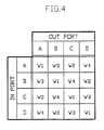
- the table given in FIG. 4 gives the complete wavelength cor respondence, where 'In' indicates the input interface where the transmitters are located and 'Out' gives the destination output node.
- the above correspondence satisfies the requirement that each input uses different wavelengths for each output and that for a given output the wavelengths used by each input are different.
- the main feature of correspondence is, however, its impact on the structure of the central switching fabric as illustrated in FIG. 5 when used with the assignment scheme for each of the demultiplexors of the switching fabric.
- the central switching fabric 150 receives the optical signals coming from the four input interfaces A, B, C and D (115-118 of FIG. 1, respectively) on four incoming optical links 151-154 respectively. Similarly, the switch fabric forwards optical signals to the four output interfaces A, B, C and D (135-138 of Fig. 1 respectively on four outgoing optical links 161-164). For clarity, only two (161 and 162) of the four outgoing optical links are represented in the figure.
- the incoming optical links 151-154 are connected to the demultiplexors at input ports 151i-154i, respectively.
- These demultiplexors use Mach-Zehnder interferometer type filters and are obtained by simple modification (permutation) of the assignment scheme shown in FIG. 3.1.
- Such demultiplexors, as described in [18] can be implemented using an integrated wave-guide structure on a silicon substrate (other types of implementations are possible, see for example [11]). This allows for small compact devices.
- the different assignment schemes for the various multiplexors (510, 520, 530, 540) of the switching fabric can be obtained by simple permutation of subgroups between branches extending from the same branch point.
- the four assignment schemes, one for each of the four demultiplexors, are also shown in FIG. 5. Notice that the assignment scheme for demultiplexor 510 is the same as the assignment scheme shown in FIG. 3.1. Also, observe that the array of outputs of the four multiplexors and the modulated wavelengths assigned thereto corresponds to the array of wavelengths shown in FIG. 4. These permutations are chosen such that the ordering of the demultiplexed wavelengths present at the n-th branches (outputs of the demultiplexors or "leaves") of the tree-structured demultiplexors 510, 520, 530 and 540 corre sponds to the ordering specified in rows A, B, C and D respectively of the wavelength correspondence table shown in FIG. 4. Other variations of table 4 would also be permissible, such as permuting the rows or columns of table 4.
- the demultiplexors 510, 520, 530 and 540 are stacked on top of each other so that their output (leaves) are vertically aligned. Notice, that the outputs of each demultiplexor lie in a corresponding horizontal plane while the inputs of each multiplexor lie in a corresponding vertical plane. Shown in FIG. 5 are four such horizontal planes (501-504) and two (505-506) of four such vertical planes, although the planes could be merely two sets of planes with planes in each set being parallel or non-intersecting within the fabric. A set of the latter planes will be referred to as non-intersecting planes.
- the outputs of the demultiplexors which are aligned along a vertical axis carry distinct wavelengths and are destined to the same output node. This means that wavelengths destined to the same output now always lie on the same vertical axis (or in the same output position in N horizontal planes) and can therefore easily be recombined while avoiding any line crossing.
- the input to output wavelength correspondence is determined by the assignment scheme used to construct each demultiplexor of the switch fabric.
- the wavelength correspondence is set. The requirement is that for any output position of the demultiplexors used in the switch fabric all the associated wavelengths must be from distinct wavelengths.
- log N N permutations of the tree structure such that, for any output position of the demultiplexors, the wavelengths are distinct, it is possible to obtain the complete wavelength correspondence by systematically constructing all the above assignment schemes of the tree structure.
- Multiplexing the wavelengths heading for a given output port simply requires that a multiplexor or coupler be vertically butted to the same output position of the horizontally stacked demultiplexors which position lies along the appropriate vertical axis, and in the N horizontal planes. Multiplexing can be achieved using either standard couplers or multiplexors symmetrical in structure to the switch demultiplexors 510, 520, 530 and 540. This approach is assumed in FIG. 5 where multiplexor 550 is symmetrical to demultiplexor 510 and, similarly, multiplexor 560 is symmetrical to demultiplexor 520.
- optical signals from different wavelengths and headed for the same output are recombined in the multiplexors, and then they are transmitted over optical fiber links (for example, over link 161 from multiplexor 550) which are connected to a corresponding output interface.
- optical fiber links for example, over link 161 from multiplexor 550
- the switch fabric is entirely passive and simply routes incoming optical signal to an appropriate output port.
- the optical signal carrying information from all input nodes and destined to a given output node is received by the corresponding output interface.
- the structure of such an output interface, for example output interface 135, is described in FIG. 6.
- the optical signals consisting of four modulated wavelengths from wavelengths W1, W2, W3 and W4 arrive over the optical fiber link 161, for example.
- the correspondence of wavelengths W1, W2, W3 and W4 to input and output ports depends on which output port they are destined for and from which input port they came. These wavelengths can be deduced by reference to the table of FIG. 4.
- wavelength W3 from input port A (151i) corresponds to output port B (162o)
- wavelength W3, from input port B (152i) corresponds to output port A.
- an incoming optical signal is first demultiplexed into its individual wavelength components (or into N distinct modulated wavelengths) in a demultiplexor 620, for example.
- the demultiplexor used can be of any type available but, as mentioned earlier, is likely to be identical to the demultiplexors used in the switch fabric so as to minimize the number of parts used in the system.
- each wavelength component is forwarded to its own receiver (630, 640, 650 and 660 for W1, W3, W2 and W4 respectively).
- Receivers 630, 640, 650 and 660 convert the optical signal into an electronic signal and provide an input to the associated clock generators 632, 642, 652 and 662.
- the clock generators provide two clock signals.
- the first one, BITCK gives the bit clock for the received signal and is used to load bits into the serial-in-parallel-out shift registers 634, 644, 654 and 664.
- the second signal, WCK is synchronized to BITCK but eight times slower. It is used to write, every cycle, the byte contained in the shift registers 634, 644, 654 and 664 into the corresponding buffers 636, 646, 656 and 666. Note that the clock signals, WCK and BITCK, provided by the different clock generators need not be in phase or even identical.
- the output node uses the clock RCK to read data bytes out of buffers 636, 646, 656 and 666 and forwards them to their final destination.
Abstract
Description
- The present invention relates to optical switching systems and in particular to wavelength division multiple access switching systems which use multiple wavelengths to route data from a multiplicity of input nodes to a multiplicity of outputs nodes. In this system the switching is achieved, in part, by means of wavelength assignment schemes and by passive multiplexing and demultiplexing devices in the switching network itself.
- In recent years the rapid increase in transmission speed introduced by the use of optical fibers has emphasized the need for high speed optical switches (see [13]) and such products are (e.g., NEC NEOX32 photonic switching system), or will be made commercially available. Multiple optical switch structures have been investigated (see [14] or a brief review), and as these structures consist of Time Division, Space Division and Wavelength Division switches. Optical switches fall into two major categories: non-integrated and integrated switches.
- Non-integrated switches are typically intended for applications which do not require high speed reconfiguration. Such systems can be simple mechanical fiber switches [3, 16] or use piezo-electric or even holographic arrays [1, 7]. Most advanced optical switches are, however, integrated switches that rely on optical couplers, splitters (demultiplexors) and combiners (multiplexors). Early work on such integrated optical switches concentrated on space switches where electronically controlled crosspoints achieved connectivity between inputs and outputs [2,4 - 6, 10, 12, 15, 19, 20]. However, as the number of wavelengths at which lasers and optical fibers could operate increased, wavelength based switches became feasible [8]. One major advantage presented by this latter class of switches is that control of the switch can now be distributed to the inputs or outputs rather than be centralized. This helps overcome the speed limitation of electronic controllers to take full advantage of the high speed available from optical technology.
- Wavelength division based switching systems fall into two categories: active and passive switches. Active switches require that the inputs/outputs of the switch are capable of adjusting the wavelength at which they are transmitting/receiving. This requires active components such as tunable lasers/filters. Examples of such systems are given in U.S. Pat. No. 3,912,876 to J.J. Muller, issued Oct. 14, 1975; in U.S. Pat. No. 3,986,020 to H. W. Kogelnik, issued Oct. 12, 1976 and in U.K. Pat. No. GB 2,043,240 A to A.M. Hill, issued Oct. 1, 1980. The use of active devices not only limits the reconfiguration time of the switches, but also requires coordinated control between all input/output connections. For example, in a system where tunable lasers are used at the inputs, the case where two inputs tune to the same wavelengths and contend for the same output must be avoided. Similar problems exist when tunable filters are used at the outputs.
- Passive optical switches avoid active components by using fixed input to output wavelength assignments so that the switching function does not require any modification of either the switch fabric or the input and output adapters, and also avoids the need for control elements. Such a system has been described in Japanese Pat. No. JA 60-237793 to K. Nagashima, issued No. 1984. This patent uses a cyclic wavelength assignment scheme which allows simultaneous communications between all inputs and all outputs. An N × N switch requires a set of N distinct wavelengths {W1,...,WN} and an input is assigned distinct wavelengths to transmit to each of the N outputs. The output wavelength assignment is cyclically shifted from input to input to ensure that no outputs receive the same wavelength from different inputs. The cyclic assignment scheme is, however, entirely independent of the type of multiplexors and demultiplexors used in the system, and does not attempt to make use of their structure and characteristics.
-
- 1. J. Bainerman, "Piezoelectric Switch Optical Signals", Laser and Applications, vol. 3, no. 12, pp. 49-51, December 1984.
- 2. R.A. Becker and W.S.C. Chang, "Electrooptical Switching in Thin Film Waveguides for a Computer Communication Bus", Applied Optics", vol. 18, no. 19, October 1979, pp. 3296-3300.
- 3. A. EL Fatatry, "1 x n Optical Fibre Switch," Electronics Letters, vol. 21, no. 14, pp. 618-619, July 1987.
- 4. P. Granestrand, B. Stoltzang, L. Thylen, K. Bergvall, W. Doldissen, H. Heinrich and D. Hoffmann, "Strictly Non-Blocking 8 x 8 Integrated Optical Switch Matrix," Electronics Letters, vol. 22, no. 15, pp. 816-818, July 1986.
- 5. K. Habara and K. Kikuchi, "Optical Time-Division Space Switches Using Tree-Structured Directional Couplers," Electronics Letters, vol. 21, no. 14, pp. 631-632, July 1985.
- 6. K. Habara and K. Kikuchi, "Geometrical Design Considerations for a Tree-Structured Optical Switch Matrix," Electronics Letters vol. 23, no. 8, pp. 376-377, April 1987.
- 7. J.P. Herriau and A. Delboulbé, B. Loiseaux and J.P. Huignard "Commutation Spatiale par Reaseau Holographique Photo-Induit", Rec. Tech. Thomson-CSF, vol. 15, no. 3, pp. 749-755, September 1983, pp. 749-775. In French.
- 8. G.R. Hill, "A Wavelength Routeing Approach to Optical Communication Networks", Telecom. Technol. J., vol. 6, no. 3, July 1988, pp. 24-31.
- 9. A. Himeno and M. Kobayashi, "Single-Mode Guided-Wave Optical Gate Matrix Switch Using Mach-Zehnder Interferometer Gates," Electronics Letters, vol. 23, no. 17, pp. 887-888, August 1987.
- 10. T. Matsunaga, K. Kikuchi and M. Ikeda, "Optical Space Division Switching System Using Laser Diode Optical Switches," Proceedings of ISS'87, 1987.
- 11. S.P. Shipley, G. Georgiou and A.C. Boucouvalas, "Compact All-Fibre Mach-Zehnder Devices," IEE Proceedings vol. 134, Pt. J., no. 3, pp. 203-207, June 1987.
- 12. R.A. Spanke, "Architecture for Large Nonblocking Optical Space Switches," IEEE J. Quantum Electron, vol. QE-23, no. 6, pp. 964-967, June 1986.
- 13. P.R. Strauss, "Optical Switches Herald a New Age of Enlightenment Data Communications," pp. 81-90, March 1988.
- 14. S.F. Su, L. Jou and J. Lenart, "A Review on Classification of Optical Switching Systems," IEEE Commun. Mag., vol. 24, no. 5, pp. 50-55, May 1986.
- 15. S. Suzuki, M. Kondoi, K. Nagashima, M. Mitsuhashi H. Nishimoto, T. Miyakawa, M. Iwasaki and Y. Ohta, "A 32-Line Optical Space Division Switching System Using 8 x 8 Optical Matrix Switches," NEC Res. and Develop., no. 87 pp. 44-50, October 1987.
- 16. M. Tatedaon, S.-I. Furukawa and H. Miyokawa, "Low-Loss Large-Scale 1 x N Optical Switch," Trans. IEICE, vol. E 70, no. 10, pp. 890-892, October 1987.
- 17. H. Toba, K. Inoue and K. Nosu, "A Conceptional Design on Optical Frequency-Division-Multiplexing Distribution Systems with Optical Tunable Filters," IEEE J. Selec. Areas Commun. vol. SAC-4, no. 9, pp. 1458-1467, December 1986.
- 18. H. Toba, K. Oda, N. Takato and K. Nosu "5 Ghz-Spaced, Eight-Channel, Guided-Wave Multi/Demultiplexer for Optical FDM Transmission Systems," Electronics Letters, vol. 23, no. 15, pp. 788-789, July 1987.
- 19. P. Li Kam Wa, J.E. Sitch, N.J. Mason, J.S. Roberts and P.N. Robson, "All Optical Multiple-Quantum-Well Waveguide Switch," Electronics Letters, vol. 21, no. 1, pp. 26-28, January 1987.
- 20. J.E. Watson, M.E. Mildbrot and T.C. Rice, "A Polarization- Independent 1 x 16 Guided-Wave Optical Switch Integrated on Lithium Niobate," IEEE J. Lightwave Technol., vol. LT-4, no. 11, pp. 1717-1721, November 1986.
- It is, therefore, an object of this invention to provide a wavelength division-based switching system with fixed wavelength assignment schemes that take advantage of the characteristics of the multiplexors and demultiplexors. This results in a simple and compact structure for the switch fabric and allows for a high level of integration.
- It is also an object of this invention to provide a passive integrated wavelength division optical switching system for a wavelength division switching network.
- It is another object of this invention to use N distinct wavelengths to allow simultaneous and contention free transmission between all input and output ports of an N × N switching system. In the description of the preferred embodiment, it is assumed that N = 2 n where n is an integer, but other values are feasible.
- It is another object of this invention to provide a wavelength assignment scheme taking into account the structure and characteristics of the demultiplexors and multiplexors to eliminate line cross-connections in the switch fabric. This assignment is, in particular, detailed for demultiplexors and multiplexors made up of Mach-Zehnder filters of the interferometer type.
- It is a further object of this invention to provide a method to arrange the demultiplexors and multiplexors used in the switch fabric to obtain an integrated and compact structure. This method is again detailed for demultiplexors and multiplexors made up of Mach-Zehnder filters of the interferometer type.
- In this invention, a number of (N) of input nodes having a plurality of sources are connected, through a central switching fabric, to a number (N) of output nodes consisting of a plurality of destinations. Each input node has the capability to send data simultaneously to all output nodes and, conversely, each output node can receive data simultaneously from all input nodes. Each input node uses an input interface to the switch fabric. The interface modulates wavelengths with data according to their intended output node. Similarly, each output node uses an output interface which identifies data received at a particular wavelength as originating from a given input node.
- In the input interface, data for each of the N output nodes are forwarded to optical transmitters (e.g., lasers) operating at different wavelengths. Each individual data stream is used to modulate its own transmitter, and the N resulting modulated wavelengths are then multiplexed and sent over a single fiber to the central switch fabric.
- In the central switch fabric the optical signals coming from each input interface are received at a switch input port, which is actually the input port of a demultiplexor of the fabric. The signals are then demultiplexed and recombined or multiplexed according to their intended output node, before being forwarded to the corresponding switch output port, which is actually the output port of a multiplexor. The input node to output node wavelength assignment ensures that no two input nodes use the same wavelength to communicate with a given output node. In addition, the wavelength assignment is such that the demultiplexors and multiplexors used in the central switch fabric can be simply stacked and butted so as to achieve an integrated and compact structure. This aspect is detailed later in the description of the preferred embodiment.
- The assignment scheme of this invention is particularly significant in that it allows for the compact structure of the switch fabric. This scheme is effected by the demultiplexors of the switching fabric. To describe the assignment scheme the method of demultiplexing N = 2 n modulated wavelengths will be described for one of the demultiplexors of the switching fabric, and the assignment scheme for each other of the N demultiplexors can easily be derived from the assignment scheme for the one demultiplexor. First, N modulated wavelengths are demultiplexed by one of the demultiplexors by separating the N modulated wavelengths at a first branch point of the demultiplexor into two distinct first subgroups, each having N/2 modulated wavelengths. Each first subgroup is then assigned to one of a pair of first branches extending from the first branch point. Each first subgroup of N/2 modulated wavelengths is further separated at a corresponding second branch point on each one of the first branches into two distinct second subgroups of N/4 modulated wavelengths resulting in four distinct second subgroups. Each second subgroup is then assigned to one of a pair of second branches extending from a corresponding second branch point. This separation continues as above until each n-th subgroup has only one modulated wavelength therein. The n-th branches of the demultiplexor are the N outputs of the demultiplexor. Thus, for the one demultiplexor an assignment scheme of subgroups to branches is formed. N modulated wavelengths are demultiplexed in the same manner as described above for each other of the N multiplexors; however, the assignment scheme for the other demultiplexors is a permutation of the assignment scheme for the one demultiplexor with the assignment scheme of subgroups to branches being different for each of the N multiplexors. The assignment scheme does, however, have certain restrictions. First, no two outputs (n-th branches) in the same output position of any two demultiplexors have the same wavelength assigned thereto. Second, each subgroup for each assignment scheme still have the same wavelengths therein. Third, and finally, each pair of subgroups assigned to branches extending from a common branch point must always be assigned to branches extending from a common branch point in any assignment scheme. Using the above assignment scheme, along with its restrictions, if the modulated wavelength appearing on each output of each demultiplexor corresponds to a modulated wavelength assigned to each output (n-th branch), there will be N horizontal planes with N distinct modulated wavelengths appearing in each plane. In addition, for any given output position in the N horizontal planes, there will be N distinct modulated wavelengths. Since the same output position in N horizontal planes lies in a vertical plane, there will be N distinct modulated wavelengths in each of the N vertical planes. The N modulated wavelengths in each vertical plane are then multiplexed so that a signal having N modulated wavelengths appears at the output port of each multiplexor.
- The optical signal coming out on the optical fiber at each output port of the switch fabric has N, one per input node, distinct modulated wavelengths. This signal is forwarded to a given output node where an output interface demultiplexes the N incoming modulated wavelengths and applies each of them to its own receiver. The original data coming from the N input nodes are then recovered and forwarded to their respective final destinations.
- The different aspects and components of the invention are better understood with reference to the detailed drawings described below. For simplicity and clarity the number N of input and output nodes has been fixed to four (4) in all drawings. It should, however, be clear that this choice is for illustration purposes only and that the concepts can be extended to any value of N.
- FIG. 1 is a block diagram of the embodiment of a switching system as described in the present invention. It consists of 4 input nodes, 4 input interfaces, a central switch fabric, 4 output interfaces and 4 output nodes. Each input interface is connected to the optical switch fabric by a dedicated optical fiber. Similarly, outgoing dedicated optical fibers connect the optical switch fabric to the 4 output interfaces which are, in turn, connected to their respective output node.
- FIG. 2 is a block diagram of an input interface suitable for use in the Wavelength Division Switching Network system shown in FIG. 1.
- FIG. 3 is a representation of a demultiplexor of the switch fabric used in this invention.
- FIG. 4 is a table showing the corresponding between wavelengths, to be modulated and transmitted, and a given input port and selected output port.
- FIG. 5 is a schematic illustration of a 4 x 4 central switching fabric with 4 demultiplexors each of whose outputs lie in a horizontal plane. Also shown are the inputs of two of the four multiplexors, each of whose inputs lie in a vertical plane.
- FIG. 6 is a block diagram of an input interface suitable for use in the switching system shown in FIG. 1. The output interface assumes again that the central switching fabric has 4 inputs and 4 outputs.
- The embodiment of the invention described below is in the context of a switching system for a digital network. An overview of the wavelength division switching network system is first provided with reference to FIG. 1 while a more detailed description is given with reference to FIGS. 2-6. For simplicity, the size of the system is taken to be N = 4, and this number is used in all figures.
- In the system described in FIG. 1, four input/output nodes (111-114/131-134) labeled A through D, have ports coupled to the central switching fabric through input/output interfaces 115-118/135-138 so that any input node may communicate with any other output node. Also schematically illustrated in FIG. 1 are the
input ports 151i-154i and output ports 160o-164o of thecentral switching fabric 150. Each of the input ports are actually input ports of demultiplexors of the switching fabric, while the output ports are actually output ports of the multiplexors of the switching fabric. Each input/output interface is, on one side, coupled to the corresponding input/output node while the other side is connected to theswitch fabric 150 by means of an otpical link. With reference to FIG. 1, optical links from input interfaces A through D are represented by the links 151-154 respectively. Similarly, the optical links from the central switching fabric to output interfaces A through D are represented by the links 161-164 respectively. In this embodiment of the switching system, the optical channels consist of single mode fibers. Other types of fibers could possibly be used. - Each input interface receives data from its input node destined to any of the N output nodes. Data destined to different output nodes are forwarded to optical transmitters operating at different wavelengths such that, for every input interface (or input port), each wavelength is uniquely associated to a given output interface (or output port), and no two input interfaces (or input ports) use the same wavelength to communicate with a given output. A particular wavelength assignment satisfying these requirements while taking into account the structure of the multiplexors and demultiplexors used is detailed below. Each input interface also receives a clock signal (e.g., MCKA for input interface 112) from its input node. This clock signal is used to generate the various clocks needed in each input interface. It should be noted that the clock signals provided by the different input nodes to the input interfaces need not be identical. In other words MCKA, MCKB, MCKC and MCKD can all be distinct. This allows the system to operate asynchronously.
- In each input interface a multiplexor multiplexes the optical signals at different wavelengths destined to different output nodes. The output of each input interface (115-118) is coupled to one of the optical fiber links (151-154). Each outgoing optical link is connected to one of the
input ports 151i-154i of the central switching fabric 150. Within thecentral switching fabric 150, the optical signal, having N modulated wavelengths from each input port is first demultiplexed into its N distinct modulated wavelengths (one for each output node). A modulated wavelength is a wavelength that has been modulated by data to be transmitted. The N distinct modulated wavelengths from all N input ports and headed for the same output node are then re-multiplexed and forwarded to the corresponding central switching fabric output port, which is an output port of a corresponding multiplexor. Each central switching fabric output port corresponds to a given output node to which it is linked by means of an optical fiber link connected to the associated output interface (links 161-164 connected to output interfaces 135-138 respectively). - The optical signal carried by each optical link (161-164) coming from the
central switching fabric 150 is received by the corresponding output interface (135-138 respectively). Each output interface demultiplexes the received optical signal into its N distinct modulated wavelengths. Each modulated wavelength carries data coming from a different input node. After the optical signals from different wavelengths have been demultiplexed and the information they carried received, data are made available to the output node which then forwards them to their final destination. Each output node provides a clock signal (RCKA, RCKB, RCKC and RCKD for output nodes 131-134 respectively) which is used to synchronize how data are read from the output interface. Note again that the clock signals from different output nodes need not be identical. - A more detailed description of the wavelength division switching system described above is now provided. The structure of an input interface is first detailed and possible implementations of the transmitters and the multiplexor are discussed. The structure of a central switching fabric based on using Mach-Zehnder filters is then briefly explained, and the wavelength assignment is presented and related to the switch fabric itself. Finally, the structure of the output interface is detailed. The descriptions are made with reference to FIG. 2 to FIG. 6 and N = 4 is assumed.
- As shown in FIG. 2 an input interface receives simultaneously four data streams, one for each output node. It is assumed that the four signals are re ceived byte-wise and are stored in separate buffers (220, 230, 240 and 250 for output nodes A, B, C and D respectively). The byte format of the received data is used for illustration purposes only and any other format could potentially be used. The write clock (WCK) for the buffers is provided by a
clock generator 210 to each of the fourbuffers clock generator 210 also generates a read clock RCK, used to read data out of the buffers, and a bit clock BITCK eight times faster than RCK (assuming byte-wide buffers). Note that, for simplicity, one common clock generator is used for the whole input interface. Different clock generators could, however, be used for data stream inputs destined to different output nodes as they need not be synchronized. - During each cycle of the RCK clock, data bytes are read from the
buffers out shift registers optical transmitters transmitters multiplexor 260 and transmitted over theoptical link 151. - Several solutions can be used to implement the transmitters and the associated multiplexor in the input interface. One solution integrates both the transmitter and the multiplexor on the same device. Such an approach is described in U.S. Pat. No. 3,908,121 to L.A. Riseberg et al., issued Sept. 23, 1975. Another possibility is to have separate sources and a multiplexor. In other words, the transmitters are, for example, individual lasers operating at different wavelengths and the multiplexor is a separate device such as the one described in U.S. Pat. No. 4,483,582 to S.K. Sheem, issued Nov. 20, 1984 or a Mach-Zehnder filter similar to those used in the switch fabric. As we shall see, this solution is potentially preferable as it reduces the number of distinct parts used in the system.
- The wavelengths assigned to the different transmitters depend on both the output node to which the transmitters send data and the input interface where they are located. In other words, a transmitter sending data to, for example, output node A is assigned a different wavelength in each input interface. This is required so that output nodes can receive data simultaneously from all input nodes. In addition to satisfying the above requirement, the assignement schemes described in this invention takes into account the structure of the central switching fabric Its purpose is best understood after describing the central switching fabric which first requires a brief explanation of the structure of the fabric.
- We assume that N = 2 n and that the N distinct wavelengths used are equispaced by frequency f. The structure of the fabric based on using Mach-Zehnder filters is now described. Such fabric has a tree structure where the multiplexing/demultiplexing function is gradually performed at the branch points of the tree, where a branch point has two branches extending therefrom.
- With each demultiplexor of the central switching fabric, the first branch point receives modulated wavelengths W1, W2, ... W2 n , and separates them into two equal first subgroups. One first subgroup contains all odd numbered modulated wavelengths W1, W3, ..., W(2 n - 1), while the other first subgroup contains even numbered modulated wavelengths W2, W4, ..., W2 n . Each first subgroup is then assigned to one of the pair of first branches extending from a first branch point. The partition is achieved by properly adjusting the length difference Δl₁ of the two arms of the first branch point (Mach-Zehnder filter (Δl₁ =

- Shown in FIG. 3.1 is a schematic illustration of a demultiplexor of the switching fabric, and the associated assignment scheme for that demultiplexor. The multiplexor in this example has an
input port 151i, onefirst branch point 30, twofirst branches first branch point 30 into two distinct first subgroups with each first subgroup having N/2 = 2 modulated wavelengths. One first subgroup has modulated wavelengths W1 and W3, while the other first subgroup has modulated wavelengths W2 and W4. The one first subgroup is assigned to afirst branch 32 extending fromfirst branch point 30, while the other first subgroup is assigned tofirst branch 34. The first subgroups are then further separated at second branch points 36 and 38 to form four distinct second subgroups. Since the second subgroups have only one modulated wavelength in each second subgroup, no further separation is required. The second subgroups are assigned to corresponding second branches 41-44. This assignment of subgroups to branches is referred to as an assignment scheme for a demultiplexor of the switching fabric. The second branches in this case (n = 2) are actually the outputs of the demultiplexor, and these outputs will all appear in one of the N horizontal planes. The position of these outputs relative to one another is referred to as the output position in the horizontal planes. For example, W1 could be said to be in the first output position while W3, W2 and W4 could be said to be in the second, third and fourth output positions respectively. As discussed in the next paragraph, other demultiplexors of the switching fabric will also have assignment schemes similar to the above assignment schemes. Further, there will be four output positions for each of the demulti plexors, and the same output position in the four horizontal planes will appear in one of the N = 4 vertical planes. Once one assignment scheme for a demultiplexor is obtained, the other assignment schemes for the demultiplexors is merely a permutation of the first assignment scheme obtained. An assignment scheme, however, is not just any permutation of the original assignment scheme obtained. There are certain restrictions. First, no two outputs (n-th branches) in the same output position of any two demultiplexors have the same wavelength assigned thereto. Second, each subgroup for each assignment scheme will have the same wavelengths therein. Third, and finally, each pair of subgroups assigned to branches extending from a common branch point must always be assigned to branches extending from the common branch point in any assignment scheme. Using the above assignment schemes, along with the restrictions, if the modulated wavelength appearing on each output of each demultiplexor corresponds to modulated wavelength assigned to each output (n-th branch), there will be N horizontal planes with N distinct modulated wavelengths appearing in each plane. It should be noted that there are as many assignment schemes as demultiplexors in the switching fabric. In addition, for any given output position in the N horizontal planes, there will be N distinct modulated wavelengths. Moreover, since the same output position in N horizontal planes lies in a vertical plane, there will be N distinct modulated wavelengths in each of the N vertical planes. The N modulated wavelengths in each vertical plane are then multiplexed so that a signal having N modulated wavelengths appears at each output port of each mutliplexor. Shown in FIG. 3.2 is a schematic illustration of one (550) of the four multiplexors of the central switching fabric. Note that the inputs 45-48 all lie in avertical plane 505. Note also that the modulated wavelengths appearing at these inputs correspond to modulated wavelengths appearing at the first output position of the four demultiplexors. See FIG. 5. - Referring to FIG. 2, there is shown a schematic illustration of the input interface (115) node A (111). The other input interfaces are similar in structure.
- With reference to FIG. 2, the
transmitters - The above correspondence satisfies the requirement that each input uses different wavelengths for each output and that for a given output the wavelengths used by each input are different. The main feature of correspondence is, however, its impact on the structure of the central switching fabric as illustrated in FIG. 5 when used with the assignment scheme for each of the demultiplexors of the switching fabric.
- Referring to FIG. 5, the
central switching fabric 150 receives the optical signals coming from the four input interfaces A, B, C and D (115-118 of FIG. 1, respectively) on four incoming optical links 151-154 respectively. Similarly, the switch fabric forwards optical signals to the four output interfaces A, B, C and D (135-138 of Fig. 1 respectively on four outgoing optical links 161-164). For clarity, only two (161 and 162) of the four outgoing optical links are represented in the figure. - The incoming optical links 151-154 are connected to the demultiplexors at
input ports 151i-154i, respectively. These demultiplexors use Mach-Zehnder interferometer type filters and are obtained by simple modification (permutation) of the assignment scheme shown in FIG. 3.1. Such demultiplexors, as described in [18]can be implemented using an integrated wave-guide structure on a silicon substrate (other types of implementations are possible, see for example [11]). This allows for small compact devices. The different assignment schemes for the various multiplexors (510, 520, 530, 540) of the switching fabric can be obtained by simple permutation of subgroups between branches extending from the same branch point. The four assignment schemes, one for each of the four demultiplexors, are also shown in FIG. 5. Notice that the assignment scheme fordemultiplexor 510 is the same as the assignment scheme shown in FIG. 3.1. Also, observe that the array of outputs of the four multiplexors and the modulated wavelengths assigned thereto corresponds to the array of wavelengths shown in FIG. 4. These permutations are chosen such that the ordering of the demultiplexed wavelengths present at the n-th branches (outputs of the demultiplexors or "leaves") of the tree-structured demultiplexors - Referring again to FIG. 5, in the switch fabric the
demultiplexors - Referring to FIG. 4, the input to output wavelength correspondence is determined by the assignment scheme used to construct each demultiplexor of the switch fabric. Once the assignment of n-th subgroups to n-th branches is complete, the wavelength correspondence is set. The requirement is that for any output position of the demultiplexors used in the switch fabric all the associated wavelengths must be from distinct wavelengths. As there are 2 log N = N permutations of the tree structure such that, for any output position of the demultiplexors, the wavelengths are distinct, it is possible to obtain the complete wavelength correspondence by systematically constructing all the above assignment schemes of the tree structure. The table of FIG. 4 illustrates this construction in the case N = 4. If one wishes to transmit data from input port B (152i) to output port D (164o), one could see from table 4, that one must modulate wavelength W2 with the data.
- Multiplexing the wavelengths heading for a given output port simply requires that a multiplexor or coupler be vertically butted to the same output position of the horizontally stacked demultiplexors which position lies along the appropriate vertical axis, and in the N horizontal planes. Multiplexing can be achieved using either standard couplers or multiplexors symmetrical in structure to the
switch demultiplexors multiplexor 550 is symmetrical to demultiplexor 510 and, similarly,multiplexor 560 is symmetrical todemultiplexor 520. In general, it can be seen that the multiplexor for output node k is identical to the demultiplexor for input node k, where k = A, B, C, or D. Such a solution presents the additional advantage of decreasing the number of parts needed in the system. - The optical signals from different wavelengths and headed for the same output are recombined in the multiplexors, and then they are transmitted over optical fiber links (for example, over
link 161 from multiplexor 550) which are connected to a corresponding output interface. It should be noted that the switch fabric is entirely passive and simply routes incoming optical signal to an appropriate output port. - After being sent over an optical fiber link leaving the
switch fabric 150, the optical signal carrying information from all input nodes and destined to a given output node is received by the corresponding output interface. The structure of such an output interface, forexample output interface 135, is described in FIG. 6. The optical signals consisting of four modulated wavelengths from wavelengths W1, W2, W3 and W4 arrive over theoptical fiber link 161, for example. As mentioned earlier, the correspondence of wavelengths W1, W2, W3 and W4 to input and output ports depends on which output port they are destined for and from which input port they came. These wavelengths can be deduced by reference to the table of FIG. 4. For example, wavelength W3 from input port A (151i) corresponds to output port B (162o), and wavelength W3, from input port B (152i) corresponds to output port A. Thus, if one wished to transmit data from input port A to output port B, one would transmit the modulated wavelength W3 (modulated by the last mentioned data) through the switchingfabric 150. - Referring to the output interface shown in FIG. 6, an incoming optical signal is first demultiplexed into its individual wavelength components (or into N distinct modulated wavelengths) in a
demultiplexor 620, for example. The demultiplexor used can be of any type available but, as mentioned earlier, is likely to be identical to the demultiplexors used in the switch fabric so as to minimize the number of parts used in the system. Once the optical signal has been demultiplexed, each wavelength component is forwarded to its own receiver (630, 640, 650 and 660 for W1, W3, W2 and W4 respectively).Receivers clock generators out shift registers buffers - Once the data bytes have been written into the
buffers buffers
Claims (10)
Applications Claiming Priority (2)
| Application Number | Priority Date | Filing Date | Title |
|---|---|---|---|
| US07/384,601 US5040169A (en) | 1989-07-25 | 1989-07-25 | Wavelength division photonic switch |
| US384601 | 1989-07-25 |
Publications (3)
| Publication Number | Publication Date |
|---|---|
| EP0410096A2 true EP0410096A2 (en) | 1991-01-30 |
| EP0410096A3 EP0410096A3 (en) | 1991-11-21 |
| EP0410096B1 EP0410096B1 (en) | 1995-02-22 |
Family
ID=23517969
Family Applications (1)
| Application Number | Title | Priority Date | Filing Date |
|---|---|---|---|
| EP90109426A Expired - Lifetime EP0410096B1 (en) | 1989-07-25 | 1990-05-18 | A wavelength division photonic switch |
Country Status (4)
| Country | Link |
|---|---|
| US (1) | US5040169A (en) |
| EP (1) | EP0410096B1 (en) |
| JP (1) | JPH0779492B2 (en) |
| DE (1) | DE69017111T2 (en) |
Cited By (3)
| Publication number | Priority date | Publication date | Assignee | Title |
|---|---|---|---|---|
| EP0571760A1 (en) * | 1992-04-29 | 1993-12-01 | International Business Machines Corporation | Space-division tunable array filter |
| WO2003040872A2 (en) * | 2001-11-02 | 2003-05-15 | Intel Corporation | Multiple-domain processing system using hierarchically orthogonal switching fabric |
| WO2014078940A1 (en) * | 2012-11-26 | 2014-05-30 | Viscore Technologies Inc. | Methods and systems for passive optical switching |
Families Citing this family (14)
| Publication number | Priority date | Publication date | Assignee | Title |
|---|---|---|---|---|
| US5528406A (en) * | 1991-08-02 | 1996-06-18 | Gpt Limited | Telecommunications switching device |
| JP2720925B2 (en) * | 1992-10-01 | 1998-03-04 | 川崎製鉄株式会社 | Low spatter wire and method of manufacturing the same |
| US5487120A (en) * | 1994-02-09 | 1996-01-23 | International Business Machines Corporation | Optical wavelength division multiplexer for high speed, protocol-independent serial data sources |
| SE502619C2 (en) * | 1994-10-11 | 1995-11-27 | Ericsson Telefon Ab L M | Optical NxN wavelength cross-coupler |
| US6680758B1 (en) * | 1997-01-16 | 2004-01-20 | Reveo, Inc. | Flat panel display and a method of fabrication |
| US6563616B1 (en) | 1999-02-21 | 2003-05-13 | Electro-Optical Sciences, Inc. | Optical demultiplexer |
| US6570872B1 (en) * | 1999-04-06 | 2003-05-27 | Nortel Networks Limited | Self-configuring distributed switch |
| US6636654B2 (en) * | 2001-03-30 | 2003-10-21 | Optical Research Associates | Programmable optical switching add/drop multiplexer |
| US6574386B1 (en) * | 2001-04-20 | 2003-06-03 | Transparent Networks, Inc. | Dynamically reconfigurable optical switching system |
| US6690848B2 (en) * | 2001-06-29 | 2004-02-10 | Nortel Networks Limited | Metropolitan photonic switch |
| US7203421B2 (en) * | 2001-09-28 | 2007-04-10 | Optical Research Associates | Littrow grating based OADM |
| US7058251B2 (en) * | 2002-06-12 | 2006-06-06 | Optical Research Associates | Wavelength selective optical switch |
| US6941073B2 (en) * | 2002-07-23 | 2005-09-06 | Optical Research Associates | East-west separable ROADM |
| JP4291281B2 (en) * | 2005-02-03 | 2009-07-08 | 富士通株式会社 | Information processing system, calculation node, and information processing system control method |
Citations (1)
| Publication number | Priority date | Publication date | Assignee | Title |
|---|---|---|---|---|
| JPS56150706A (en) * | 1980-04-23 | 1981-11-21 | Nippon Telegr & Teleph Corp <Ntt> | Multiple optical branching filter |
Family Cites Families (5)
| Publication number | Priority date | Publication date | Assignee | Title |
|---|---|---|---|---|
| JPS6177490A (en) * | 1984-09-22 | 1986-04-21 | Nippon Telegr & Teleph Corp <Ntt> | Light matrix switch |
| JPH061318B2 (en) * | 1985-08-09 | 1994-01-05 | 日本電信電話株式会社 | Wavelength division multiplexing optical switch |
| JPS6290626A (en) * | 1985-10-17 | 1987-04-25 | Nec Corp | Optical switch circuit |
| JPS6290627A (en) * | 1985-10-17 | 1987-04-25 | Nec Corp | Optical switch circuit |
| JPS63238728A (en) * | 1987-03-26 | 1988-10-04 | Shimadzu Corp | Optical transmitting equipment |
-
1989
- 1989-07-25 US US07/384,601 patent/US5040169A/en not_active Expired - Lifetime
-
1990
- 1990-05-18 EP EP90109426A patent/EP0410096B1/en not_active Expired - Lifetime
- 1990-05-18 DE DE69017111T patent/DE69017111T2/en not_active Expired - Lifetime
- 1990-07-25 JP JP2195098A patent/JPH0779492B2/en not_active Expired - Lifetime
Patent Citations (1)
| Publication number | Priority date | Publication date | Assignee | Title |
|---|---|---|---|---|
| JPS56150706A (en) * | 1980-04-23 | 1981-11-21 | Nippon Telegr & Teleph Corp <Ntt> | Multiple optical branching filter |
Non-Patent Citations (4)
| Title |
|---|
| ELECTRONIC DESIGN, vol. 36, no. 21, 22nd September 1988, page 35; B.W. PHILLIPS: "Optical crossbar switch works at gigahertz rate" * |
| IEEE COMMUNICATIONS MAGAZINE, vol. 29, no. 3, March 1989, pages 22-30; S.S. WAGNER et al.: "WDM applications in broadband telecommunication networks" * |
| INFOCOM 1988, New Orleans, Louisiana, 27th - 31st March 1988, pages 354-361; G.R. HILL: "A wavelength routing approach to optical communications networks" * |
| PATENT ABSTRACTS OF JAPAN, vol. 6, no. 30 (P-103)[908], 23rd February 1982; & JP-A-56 150 706 (NIPPON DENSHIN DENWA KOSHA) 21-11-1981 * |
Cited By (7)
| Publication number | Priority date | Publication date | Assignee | Title |
|---|---|---|---|---|
| EP0571760A1 (en) * | 1992-04-29 | 1993-12-01 | International Business Machines Corporation | Space-division tunable array filter |
| WO2003040872A2 (en) * | 2001-11-02 | 2003-05-15 | Intel Corporation | Multiple-domain processing system using hierarchically orthogonal switching fabric |
| WO2003040872A3 (en) * | 2001-11-02 | 2004-03-04 | Intel Corp | Multiple-domain processing system using hierarchically orthogonal switching fabric |
| US7310319B2 (en) | 2001-11-02 | 2007-12-18 | Intel Corporation | Multiple-domain processing system using hierarchically orthogonal switching fabric |
| US7808989B2 (en) | 2001-11-02 | 2010-10-05 | Oleg Awsienko | Multiple-domain processing system using hierarchically orthogonal switching fabric |
| WO2014078940A1 (en) * | 2012-11-26 | 2014-05-30 | Viscore Technologies Inc. | Methods and systems for passive optical switching |
| EP2923455A4 (en) * | 2012-11-26 | 2016-08-31 | Viscore Technologies Inc | Methods and systems for passive optical switching |
Also Published As
| Publication number | Publication date |
|---|---|
| JPH0360599A (en) | 1991-03-15 |
| EP0410096A3 (en) | 1991-11-21 |
| US5040169A (en) | 1991-08-13 |
| JPH0779492B2 (en) | 1995-08-23 |
| DE69017111T2 (en) | 1995-08-10 |
| DE69017111D1 (en) | 1995-03-30 |
| EP0410096B1 (en) | 1995-02-22 |
Similar Documents
| Publication | Publication Date | Title |
|---|---|---|
| Danielsen et al. | Wavelength conversion in optical packet switching | |
| EP0410096B1 (en) | A wavelength division photonic switch | |
| EP0382431B1 (en) | Communications network | |
| US5878177A (en) | Layered switch architectures for high-capacity optical transport networks | |
| US4821255A (en) | Cross-connection of wavelength-division-multiplexed high speed optical channels | |
| KR101978191B1 (en) | Scalable optical switches and switching modules | |
| EP1017242B1 (en) | Optical cross-connect architecture for WDM telecommunication systems | |
| US6243178B1 (en) | Optical crossbar network using wavelength division multiplexing an optical crossbar exchange | |
| US5627925A (en) | Non-blocking optical cross-connect structure for telecommunications network | |
| JP2989269B2 (en) | Cross connection for optical networks | |
| US5930016A (en) | Upgradable modular wavelength division multiplexer | |
| US7394806B2 (en) | Distributed space-time-space switch | |
| US11190860B2 (en) | Switch with a shuffle | |
| US7764882B2 (en) | Optical packet tray router | |
| US20020131678A1 (en) | Wavelength-modular optical cross-connect switch | |
| US7206509B2 (en) | Method and apparatus for temporally shifting one or more packets using wavelength selective delays | |
| Gambini | State of the art of photonic packet switched networks | |
| US20040258411A1 (en) | Node for an optical network | |
| Thompson et al. | Elementary photonic switching modules in three divisions | |
| Masetti | System functionalities and architectures in photonic packet switching | |
| JP2690310B2 (en) | Optical switching system | |
| CA2310856A1 (en) | Time-slotted optical space switch | |
| JPH06121357A (en) | Optical switch circuit | |
| JPH08293871A (en) | Optical atm switch | |
| EP0733298B1 (en) | A cross-connect for an optical network |
Legal Events
| Date | Code | Title | Description |
|---|---|---|---|
| PUAI | Public reference made under article 153(3) epc to a published international application that has entered the european phase |
Free format text: ORIGINAL CODE: 0009012 |
|
| AK | Designated contracting states |
Kind code of ref document: A2 Designated state(s): DE FR GB |
|
| 17P | Request for examination filed |
Effective date: 19901213 |
|
| PUAL | Search report despatched |
Free format text: ORIGINAL CODE: 0009013 |
|
| AK | Designated contracting states |
Kind code of ref document: A3 Designated state(s): DE FR GB |
|
| 17Q | First examination report despatched |
Effective date: 19930914 |
|
| GRAA | (expected) grant |
Free format text: ORIGINAL CODE: 0009210 |
|
| AK | Designated contracting states |
Kind code of ref document: B1 Designated state(s): DE FR GB |
|
| REF | Corresponds to: |
Ref document number: 69017111 Country of ref document: DE Date of ref document: 19950330 |
|
| ET | Fr: translation filed | ||
| PLBE | No opposition filed within time limit |
Free format text: ORIGINAL CODE: 0009261 |
|
| STAA | Information on the status of an ep patent application or granted ep patent |
Free format text: STATUS: NO OPPOSITION FILED WITHIN TIME LIMIT |
|
| 26N | No opposition filed | ||
| PGFP | Annual fee paid to national office [announced via postgrant information from national office to epo] |
Ref country code: FR Payment date: 19960507 Year of fee payment: 7 |
|
| PG25 | Lapsed in a contracting state [announced via postgrant information from national office to epo] |
Ref country code: FR Free format text: LAPSE BECAUSE OF NON-PAYMENT OF DUE FEES Effective date: 19980130 |
|
| REG | Reference to a national code |
Ref country code: FR Ref legal event code: ST |
|
| REG | Reference to a national code |
Ref country code: GB Ref legal event code: IF02 |
|
| PGFP | Annual fee paid to national office [announced via postgrant information from national office to epo] |
Ref country code: GB Payment date: 20040506 Year of fee payment: 15 |
|
| PG25 | Lapsed in a contracting state [announced via postgrant information from national office to epo] |
Ref country code: GB Free format text: LAPSE BECAUSE OF NON-PAYMENT OF DUE FEES Effective date: 20050518 |
|
| GBPC | Gb: european patent ceased through non-payment of renewal fee |
Effective date: 20050518 |
|
| PGFP | Annual fee paid to national office [announced via postgrant information from national office to epo] |
Ref country code: DE Payment date: 20090528 Year of fee payment: 20 |
|
| PG25 | Lapsed in a contracting state [announced via postgrant information from national office to epo] |
Ref country code: DE Free format text: LAPSE BECAUSE OF EXPIRATION OF PROTECTION Effective date: 20100518 |