EP0409213A2 - Amplifiying compensation circuit for semiconductor pressure sensor - Google Patents
Amplifiying compensation circuit for semiconductor pressure sensor Download PDFInfo
- Publication number
- EP0409213A2 EP0409213A2 EP90113791A EP90113791A EP0409213A2 EP 0409213 A2 EP0409213 A2 EP 0409213A2 EP 90113791 A EP90113791 A EP 90113791A EP 90113791 A EP90113791 A EP 90113791A EP 0409213 A2 EP0409213 A2 EP 0409213A2
- Authority
- EP
- European Patent Office
- Prior art keywords
- resistor
- pressure sensor
- operational amplifier
- circuit
- temperature
- Prior art date
- Legal status (The legal status is an assumption and is not a legal conclusion. Google has not performed a legal analysis and makes no representation as to the accuracy of the status listed.)
- Granted
Links
Images


Classifications
-
- G—PHYSICS
- G01—MEASURING; TESTING
- G01L—MEASURING FORCE, STRESS, TORQUE, WORK, MECHANICAL POWER, MECHANICAL EFFICIENCY, OR FLUID PRESSURE
- G01L19/00—Details of, or accessories for, apparatus for measuring steady or quasi-steady pressure of a fluent medium insofar as such details or accessories are not special to particular types of pressure gauges
- G01L19/02—Arrangements for preventing, or for compensating for, effects of inclination or acceleration of the measuring device; Zero-setting means
-
- G—PHYSICS
- G01—MEASURING; TESTING
- G01L—MEASURING FORCE, STRESS, TORQUE, WORK, MECHANICAL POWER, MECHANICAL EFFICIENCY, OR FLUID PRESSURE
- G01L1/00—Measuring force or stress, in general
- G01L1/20—Measuring force or stress, in general by measuring variations in ohmic resistance of solid materials or of electrically-conductive fluids; by making use of electrokinetic cells, i.e. liquid-containing cells wherein an electrical potential is produced or varied upon the application of stress
- G01L1/22—Measuring force or stress, in general by measuring variations in ohmic resistance of solid materials or of electrically-conductive fluids; by making use of electrokinetic cells, i.e. liquid-containing cells wherein an electrical potential is produced or varied upon the application of stress using resistance strain gauges
- G01L1/2268—Arrangements for correcting or for compensating unwanted effects
- G01L1/2281—Arrangements for correcting or for compensating unwanted effects for temperature variations
-
- G—PHYSICS
- G01—MEASURING; TESTING
- G01L—MEASURING FORCE, STRESS, TORQUE, WORK, MECHANICAL POWER, MECHANICAL EFFICIENCY, OR FLUID PRESSURE
- G01L9/00—Measuring steady of quasi-steady pressure of fluid or fluent solid material by electric or magnetic pressure-sensitive elements; Transmitting or indicating the displacement of mechanical pressure-sensitive elements, used to measure the steady or quasi-steady pressure of a fluid or fluent solid material, by electric or magnetic means
- G01L9/02—Measuring steady of quasi-steady pressure of fluid or fluent solid material by electric or magnetic pressure-sensitive elements; Transmitting or indicating the displacement of mechanical pressure-sensitive elements, used to measure the steady or quasi-steady pressure of a fluid or fluent solid material, by electric or magnetic means by making use of variations in ohmic resistance, e.g. of potentiometers, electric circuits therefor, e.g. bridges, amplifiers or signal conditioning
- G01L9/04—Measuring steady of quasi-steady pressure of fluid or fluent solid material by electric or magnetic pressure-sensitive elements; Transmitting or indicating the displacement of mechanical pressure-sensitive elements, used to measure the steady or quasi-steady pressure of a fluid or fluent solid material, by electric or magnetic means by making use of variations in ohmic resistance, e.g. of potentiometers, electric circuits therefor, e.g. bridges, amplifiers or signal conditioning of resistance-strain gauges
- G01L9/045—Measuring steady of quasi-steady pressure of fluid or fluent solid material by electric or magnetic pressure-sensitive elements; Transmitting or indicating the displacement of mechanical pressure-sensitive elements, used to measure the steady or quasi-steady pressure of a fluid or fluent solid material, by electric or magnetic means by making use of variations in ohmic resistance, e.g. of potentiometers, electric circuits therefor, e.g. bridges, amplifiers or signal conditioning of resistance-strain gauges with electric temperature compensating means
Definitions
- the invention is an amplifying compensation circuit for a semiconductor pressure sensor. More particularly, the invention relates to an amplifying compensation circuit which realizes a high precision semiconductor pressure sensor with a small number of circuit elements.
- a semiconductor pressure sensor generates a voltage or a set of voltages which are dependent on the pressure applied to the sensor. Circuitry is provided to amplify the generated voltage and to adjust the generated voltage.
- the voltage generated by a semiconductor pressure sensor may vary with the temperature. Therefore, circuitry associated with the semiconductor pressure sensor must compensate for temperature induced voltage changes to achieve accurate pressure readings.
- the zero point is the semiconductor pressure sensor output voltage when no external pressure or only a background pressure is applied to the pressure sensor.
- the zero point may vary with the temperature. Therefore, circuitry should be provided to compensate for the temperature induced changes in the zero point.
- the setting of the zero point should be adjustable to allow the pressure sensor to operate over a wide range of conditions.
- Resistor 52 compensates for temperature induced voltage changes.
- Resistor 52 is a diffusion resistor which has a positive temperature dependency.
- Resistor 52 gives a positive temperature dependency to the degree of amplification of the rear stage differential amplifier and, therefore, compensates the negative temperature dependency of the strain gauge bridge.
- the resistor 7 serves as an adjustment resistor.
- Sensitivity adjustment is carried out by adjusting the resistance of the resistor 1 until the amplification of the circuit is a predetermined value.
- the output voltage Vd of an operational amplifier 204 is added to the sensor output voltage V out of the rear stage differential amplifier including the operational amplifier 203.
- the potential and temperature characteristics of the output voltage Vd of the amplifier 204 are selected to perform zero point adjustment and zero point temperature dependent change compensation.
- resistors 50 and 51 have temperature dependent resistance.
- the resistances of resistors 10 and 11, respectively connected in parallel with resistors 50 and 51, are selected to insure a predetermined temperature characteristic of the output voltage Vd of the operational amplifier 204.
- the zero point adjustment and the zero point temperature characteristic compensation are carried out with the aid of the operational amplifier 204 and its peripheral resistors 8-13, 50, and 51.
- the adjustments are carried out in the order of: sensitivity temperature characteristic compensation; sensitivity adjustment; zero point temperature characteristic compensation; and zero point adjustment.
- the adjustments are separately performed. Hence, in the adjustments, high adjustment accuracy can be obtained relatively easily.
- the number of elements in the circuit of FIG. 4 is large; four operational amplifiers, thirteen resistors, and three temperature dependent resistors are used.
- the large number of elements will obstruct miniaturization of the sensor, and will obstruct integration of all the elements of the sensor on a single silicon chip.
- FIG. 5 shows another example of an amplifying compensation circuit having four compensation and adjustment functions.
- the output voltage of a bridge 100 consisting of strain gauges 101-104 is amplified by a differential amplifier made up of an operational amplifier 205 and resistors 15-18.
- Temperature dependent voltage changes are compensated for by means of resistors 14 and 53 connected between the positive terminal of the power source and the strain gauge bridge.
- the resistor 53 has a negative temperature dependency.
- Resistor 53 may be a thermistor.
- the arrangement of resistors 14 and 53 gives a positive temperature dependency to the potential at the connecting point A of the strain gauges.
- the positive drive voltage developed between the supply voltage drive terminals of the bridge 100 compensates the negative temperature dependency of the pressure sensitivity of the strain gauges 101-104.
- the resistance of the resistor 18 is selected to set the amplification to a predetermined value to adjust the sensitivity of the sensor.
- Zero point adjustment is performed by adjusting the resistances of resistors 19 and 20 which are connected to the resistor 17 of the differential amplifier.
- the number of elements is not so large; one operational amplifier, seven resistors, and one temperature dependent resistor are used.
- the sensitivity adjustment, the zero point adjustment, and the zero point temperature characteristic are not performed separately. Without separation, it is difficult to perform the adjustments with high accuracy.
- the zero point temperature characteristic compensation range is narrow, because the range is limited by the temperature dependency of the bridge output in-phase voltage. Hence, compensation cannot be achieved if the zero point temperature dependency of the bridge output fluctuates greatly.
- the bridge drive voltage becomes lower than the sensor supply voltage decreasing the bridge output signal.
- Japanese Patent Application (OPI) No. 217375/1984 discloses a circuit similar to the above-described circuit.
- the circuit disclosed has a smaller number of components than the circuit shown in FIG. 4.
- it is disadvantageous in that the zero point temperature compensation range is narrow, and the characteristic compensations are not separated from one another.
- an object of this invention is to solve the above-described problems.
- a semiconductor pressure sensor having first and second terminals connected respectively to first and second potentials, and pressure sensing means interconnected with the first and second terminals for generating first and second voltages.
- the difference of the first and second voltages is dependent on at least one pressure to be sensed.
- a voltage follower circuit receives the first voltage and changes the impedance of the first voltage.
- Amplifier means amplify the difference between the first and second voltages, and the amplifier means comprise an operational amplifier with first and second inputs and a feedback circuit with a temperature dependent resistor.
- Means for adjusting the sensitivity of the pressure sensor comprise a resistor with adjustable resistance connected between the pressure sensing means and the first input of the operational amplifier.
- Means for compensating for temperature induced fluctuations in the zero point of the pressure sensor comprise at least one temperature dependent resistor connected between the first input of the operational amplifier and the first terminal, and at least one temperature dependent resistor connected between the first input of the operational amplifier and the second terminal.
- Means for adjusting the zero point comprise at least one resistor with an adjustable resistance connected between the first input of the operational amplifier and the first terminal, and at least one resistor with an adjustable resistance connected between the first input of the operational amplifier and the second terminal.
- the voltage follower circuit comprises one operational amplifier. One output voltage, in the form of low output impedance, is applied directly to the differential amplifier circuit.
- the voltage follower circuit increases the output impedance of the other output voltage before the output voltage is applied to the operational amplifier. Therefore, the voltage follower circuit prevents the interference in characteristic between the differential amplifier circuit and the bridge circuit.
- sensitivity adjustments are carried out by adjusting the resistance of an input resistor. Sensitivity temperature compensation is performed with the aid of feedback resistors where at least one resistor has a positive temperature dependency. Zero point adjustment is carried out with the resistors connected between the inversion input terminal and the positive and negative power source terminals. Zero point temperature compensation is performed with the aid of the resistors connected between the inversion input terminal and the positive and negative power source terminals where two resistors have a high temperature dependency.
- the sensitivity temperature compensation, the sensitivity adjustment, the zero point adjustment, and the zero point temperature compensation are carried out independently.
- resistors 50-58 are temperature dependent resistors.
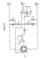
- FIG. 1 shows a first embodiment of the semiconductor pressure sensor circuit. Strain gauges 101 through 104 form a bridge 100 on a silicon diaphragm. Strain gauges 101 through 104 are positioned on the diaphragm so that a voltage signal is developed across differential output terminals C and D of the bridge 100 in response to the application of pressure.
- Terminal D is connected to the non-inversion input terminal of an operational amplifier 206.
- the inversion input terminal of operational amplifier 206 is connected to its output terminal, thus forming a voltage follower circuit.
- the output terminal of the operational amplifier 206 is connected through an adjustable resistor 21 to the inversion input terminal of an operational amplifier 207.
- the non-inversion input terminal of the differential amplifier 207 is connected to terminal C of the bridge 100.
- the inversion input terminal of the operational amplifier 207 is also connected through a resistor 22 to a power source terminal E.
- An adjustable resistor 24 and a temperature dependent resistor 54, connected in series, are connected between the inversion input terminal of the operational amplifier 207 and the power source terminal E.
- the adjustable resistor 22 is, thus, shunted by the two resistors 24 and 54 connected in series.
- the inversion input terminal of the operational amplifier 207 is further connected through a resistor 23 to a ground terminal G.
- the resistor 23 is shunted by a series circuit of an adjustable resistor 25 and a temperature dependent resistor 55.
- a parallel circuit of a resistor 56 having a positive temperature dependency and an adjustable resistor 26 is connected between the inversion input terminal of operational amplifier 207 and the output terminal of operational amplifier 207.
- the output terminal of operational amplifier 207 is the output terminal F of the semiconductor pressure sensor.
- a sensor output voltage V out is provided at terminal F.
- Output voltages Vi- is applied to the voltage follower circuit comprising operational amplifier 206.
- the output voltage Vi+ in the form of high output impedance, is applied directly to the operational amplifier 207.
- the voltage follower circuit decreases the output impedance of the output voltage Vi- before the output voltage Vi- is applied to the operational amplifier 207. Therefore, the voltage follower circuit prevents the interference in characteristic between the differential amplifier circuit comprising operational amplifier 207 and the bridge 100.
- the difference between the potentials Vi- and Vi+ is amplified by the operational amplifier 207 with the aid of the peripheral resistors.
- Resistor 56 is connected, together with resistor 26, as a parallel circuit of feedback resistors between the output terminal and the inversion input terminal of the operational amplifier 207.
- the amplification of the differential amplifier 207 has a positive temperature dependency because of the temperature dependent resistor 56.
- the positive temperature dependency is utilized to compensate the negative temperature dependency of the bridge 100.
- the amplification of operational amplifier 207 and, accordingly, the sensitivity may be adjusted by changing the resistance of the resistor 21.
- the series circuit of the adjustable resistor 24 and temperature dependent resistor 54 and the series circuit of the adjustable resistor 25 and temperature dependent resistor 55 are provided for zero point temperature characteristic compensation.
- Resistors 54 and 55 both have a positive temperature dependency.
- Current flows from the power source terminal E through the series circuit of the resistors 24 and 54 and the parallel circuit of the feedback resistors 26 and 56 to the output terminal F of the operational amplifier 207 decreasing the sensor output voltage V out .
- the decreasing current has a negative temperature dependency being affected by the resistor 54, thus giving a positive temperature dependency to the sensor output voltage V out .
- the adjustable resistors 22 and 23 are provided for zero point adjustment. Current flows from the power source terminal E through the resistor 22 and the parallel circuit of the feedback resistors 26 and 56 to the output terminal F of the operational amplifier 207, thus decreasing the sensor output voltage V out . Conversely, current flows from the output terminal F of the operational amplifier 207 through the parallel circuit of the feedback resistors 26 and 56 and the resistor 23 to the ground terminal G, thus increasing the sensor output voltage V out .
- the zero point of the sensor output voltage V out is obtained by adjusting the resistances of the resistors 22 and 23.
- V out Vi+ + (Rx/R21)(Vi+ - Vi-) - (Vcc - Vi+)(Rx/R22) + Vi+(Rx/R23) - (Vcc - Vi+) ⁇ Rx/(R24 + R54) ⁇ + Vi+ ⁇ Rx/(R25 + R55) ⁇ (1)
- Rx R56 x R26/(R56 + R26) (2) and Vcc is the supply voltage
- the second term of the right side is the bridge 100 output amplified; the third term is the current flowing in the resistor 22; the fourth term is the current flow in the resistor 23; the fifth term is the current flowing in the resistors 24 and 54; and the sixth term is the current flowing in the resistor 25 and 55.
- the second term of the right side is for sensitivity adjustment, and sensitivity temperature characteristic (compensation) adjustment; the third and fourth terms are for zero point adjustment; and the fifth and sixth terms are for zero point temperature (compensation) adjustment.
- the circuit elements concerning sensitivity and the circuit elements concerning zero point are separate. Therefore, the sensitivity adjustment and the sensitivity temperature compensation are independent of the zero point adjustment and the zero point temperature characteristic compensation. Therefore, high adjustment accuracy can be easily obtained.
- zero point temperature characteristic compensation is intended to mean the compensation of a temperature gradient.
- the bend of the temperature character can also be compensated.
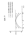
- FIG. 2 shows temperature gradient compensated temperature characteristics for different resistances of the resistors 24 and 25. As is apparent from FIG. 2, a curved temperature characteristic can be changed into a flat temperature characteristic by changing the resistances of resistors 24 and 25 in a balancing mode.
- a curved sensitivity temperature characteristic can also be changed into a flat sensitivity temperature characteristic by changing the temperature characteristic of resistor 56.
- the temperature characteristic of the resistor 56 can be changed by adjusting the dosage of impurities. Therefore, the curved sensitivity temperature characteristic of the sensor output V out can be changed into a flat one.
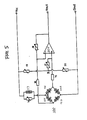
- FIG. 3 shows a second embodiment of the invention, which has the same effects as the first embodiment shown in FIG. 1.
- the zero point adjustment and the zero point temperature characteristic compensation are carried out by setting the resistances of resistors 27 through 30 to suitable values.
- the semiconductor pressure sensor has the following effects or merits:
Abstract
Description
- The invention is an amplifying compensation circuit for a semiconductor pressure sensor. More particularly, the invention relates to an amplifying compensation circuit which realizes a high precision semiconductor pressure sensor with a small number of circuit elements.
- A semiconductor pressure sensor generates a voltage or a set of voltages which are dependent on the pressure applied to the sensor. Circuitry is provided to amplify the generated voltage and to adjust the generated voltage.
- The voltage generated by a semiconductor pressure sensor may vary with the temperature. Therefore, circuitry associated with the semiconductor pressure sensor must compensate for temperature induced voltage changes to achieve accurate pressure readings.
- Different semiconductor pressure sensors will have slightly different voltage characteristics depending on the manufacturing attributes. Therefore, the sensitivity of the pressure sensor is adjusted.
- The zero point is the semiconductor pressure sensor output voltage when no external pressure or only a background pressure is applied to the pressure sensor. The zero point may vary with the temperature. Therefore, circuitry should be provided to compensate for the temperature induced changes in the zero point.
- The setting of the zero point should be adjustable to allow the pressure sensor to operate over a wide range of conditions.
- FIG. 4 shows one example of a circuit for performing the two compensations and two adjustments discussed above. The output voltage of a
bridge 100 made up of strain gauges 101-104 is dependent on the pressure applied to the strain gauges 101-104. The output voltage is amplified by a front stage differential amplifier comprisingoperational amplifiers operational amplifier 203 and resistors 4-7 and 52. The output voltage thus amplified is provided as an output Vout. -
Resistor 52 compensates for temperature induced voltage changes.Resistor 52 is a diffusion resistor which has a positive temperature dependency.Resistor 52 gives a positive temperature dependency to the degree of amplification of the rear stage differential amplifier and, therefore, compensates the negative temperature dependency of the strain gauge bridge. In the compensation circuit, theresistor 7 serves as an adjustment resistor. - Sensitivity adjustment is carried out by adjusting the resistance of the resistor 1 until the amplification of the circuit is a predetermined value.
- The output voltage Vd of an
operational amplifier 204 is added to the sensor output voltage Vout of the rear stage differential amplifier including theoperational amplifier 203. The potential and temperature characteristics of the output voltage Vd of theamplifier 204 are selected to perform zero point adjustment and zero point temperature dependent change compensation. - In FIG. 4,
resistors resistors resistors operational amplifier 204. As is apparent from the above description, the zero point adjustment and the zero point temperature characteristic compensation are carried out with the aid of theoperational amplifier 204 and its peripheral resistors 8-13, 50, and 51. - With amplifying compensation, the adjustments are carried out in the order of: sensitivity temperature characteristic compensation; sensitivity adjustment; zero point temperature characteristic compensation; and zero point adjustment. The adjustments are separately performed. Hence, in the adjustments, high adjustment accuracy can be obtained relatively easily.
- However, the number of elements in the circuit of FIG. 4 is large; four operational amplifiers, thirteen resistors, and three temperature dependent resistors are used. The large number of elements will obstruct miniaturization of the sensor, and will obstruct integration of all the elements of the sensor on a single silicon chip.
- FIG. 5 shows another example of an amplifying compensation circuit having four compensation and adjustment functions. The output voltage of a
bridge 100 consisting of strain gauges 101-104 is amplified by a differential amplifier made up of anoperational amplifier 205 and resistors 15-18. - Temperature dependent voltage changes are compensated for by means of
resistors 14 and 53 connected between the positive terminal of the power source and the strain gauge bridge. Theresistor 53 has a negative temperature dependency.Resistor 53 may be a thermistor. The arrangement ofresistors 14 and 53 gives a positive temperature dependency to the potential at the connecting point A of the strain gauges. The positive drive voltage developed between the supply voltage drive terminals of thebridge 100 compensates the negative temperature dependency of the pressure sensitivity of the strain gauges 101-104. - The resistance of the
resistor 18 is selected to set the amplification to a predetermined value to adjust the sensitivity of the sensor. - Zero point temperature characteristic compensation is carried out by setting the resistance of the
resistor 17 to compensate the temperature dependency of the zero point of thebridge 100 output. - Zero point adjustment is performed by adjusting the resistances of
resistors resistor 17 of the differential amplifier. - When the resistance of the
resistor 17 is high, the positive temperature dependency of the bridge output in-phase potential is outputted unchanged, thus, giving a positive temperature dependency to the output Vout of the circuit. As the resistance of theresistor 17 decreases, the potential at a connecting point B of theresistors differential amplifier 205, thus, making the temperature dependency of the sensor output Vout more negative. - In the circuit of FIG. 5, the number of elements is not so large; one operational amplifier, seven resistors, and one temperature dependent resistor are used. However, the sensitivity adjustment, the zero point adjustment, and the zero point temperature characteristic are not performed separately. Without separation, it is difficult to perform the adjustments with high accuracy. Furthermore, the zero point temperature characteristic compensation range is narrow, because the range is limited by the temperature dependency of the bridge output in-phase voltage. Hence, compensation cannot be achieved if the zero point temperature dependency of the bridge output fluctuates greatly. In addition, because of the voltage drop across the parallel circuit of the
resistors 14 and 53, the bridge drive voltage becomes lower than the sensor supply voltage decreasing the bridge output signal. - Japanese Patent Application (OPI) No. 217375/1984 (the term "OPI" as used herein means an "unexamined published application") discloses a circuit similar to the above-described circuit. The circuit disclosed has a smaller number of components than the circuit shown in FIG. 4. However, it is disadvantageous in that the zero point temperature compensation range is narrow, and the characteristic compensations are not separated from one another.
- Accordingly, an object of this invention is to solve the above-described problems.
- Additional objects and advantages of the invention will be set forth in part in the description which follows and in part will be obvious from the description, or may be learned by practice of the invention. The objects and advantages of the invention may be realized and attained by means of the instrumentalities and combinations particularly pointed out in the appended claims.
- The foregoing objects of the invention have been achieved by the provision of a semiconductor pressure sensor having first and second terminals connected respectively to first and second potentials, and pressure sensing means interconnected with the first and second terminals for generating first and second voltages. The difference of the first and second voltages is dependent on at least one pressure to be sensed. A voltage follower circuit receives the first voltage and changes the impedance of the first voltage. Amplifier means amplify the difference between the first and second voltages, and the amplifier means comprise an operational amplifier with first and second inputs and a feedback circuit with a temperature dependent resistor. Means for adjusting the sensitivity of the pressure sensor comprise a resistor with adjustable resistance connected between the pressure sensing means and the first input of the operational amplifier. Means for compensating for temperature induced fluctuations in the zero point of the pressure sensor comprise at least one temperature dependent resistor connected between the first input of the operational amplifier and the first terminal, and at least one temperature dependent resistor connected between the first input of the operational amplifier and the second terminal. Means for adjusting the zero point comprise at least one resistor with an adjustable resistance connected between the first input of the operational amplifier and the first terminal, and at least one resistor with an adjustable resistance connected between the first input of the operational amplifier and the second terminal.
- The voltage follower circuit comprises one operational amplifier. One output voltage, in the form of low output impedance, is applied directly to the differential amplifier circuit. The voltage follower circuit increases the output impedance of the other output voltage before the output voltage is applied to the operational amplifier. Therefore, the voltage follower circuit prevents the interference in characteristic between the differential amplifier circuit and the bridge circuit.
- In the differential amplifier circuit, comprising at least one operational amplifier, sensitivity adjustments are carried out by adjusting the resistance of an input resistor. Sensitivity temperature compensation is performed with the aid of feedback resistors where at least one resistor has a positive temperature dependency. Zero point adjustment is carried out with the resistors connected between the inversion input terminal and the positive and negative power source terminals. Zero point temperature compensation is performed with the aid of the resistors connected between the inversion input terminal and the positive and negative power source terminals where two resistors have a high temperature dependency.
- The sensitivity temperature compensation, the sensitivity adjustment, the zero point adjustment, and the zero point temperature compensation are carried out independently.
- The accompanying drawings, which are incorporated in and constitute a part of this specification illustrate embodiments of the invention and, together with the description, serve to explain the principles of the invention.
- In the figures, like references numbers refer to similar or like parts.
- FIG. 1 is a circuit diagram showing a first embodiment of the pressure sensor.
- FIG. 2 is a graphical representation indicating temperature gradient compensated temperature characteristics with the resistances of
resistors - FIG. 3 is a circuit diagram showing a second embodiment of the pressure sensor.
- FIG. 4 and 5 are circuit diagrams showing different examples of conventional amplifying compensation circuits in a pressure sensor.
- In the figures, resistors 50-58 are temperature dependent resistors.
- FIG. 1 shows a first embodiment of the semiconductor pressure sensor circuit. Strain gauges 101 through 104 form a
bridge 100 on a silicon diaphragm. Strain gauges 101 through 104 are positioned on the diaphragm so that a voltage signal is developed across differential output terminals C and D of thebridge 100 in response to the application of pressure. - Terminal D is connected to the non-inversion input terminal of an
operational amplifier 206. The inversion input terminal ofoperational amplifier 206 is connected to its output terminal, thus forming a voltage follower circuit. - The output terminal of the
operational amplifier 206 is connected through anadjustable resistor 21 to the inversion input terminal of anoperational amplifier 207. The non-inversion input terminal of thedifferential amplifier 207 is connected to terminal C of thebridge 100. The inversion input terminal of theoperational amplifier 207 is also connected through a resistor 22 to a power source terminal E. Anadjustable resistor 24 and a temperaturedependent resistor 54, connected in series, are connected between the inversion input terminal of theoperational amplifier 207 and the power source terminal E. The adjustable resistor 22 is, thus, shunted by the tworesistors operational amplifier 207 is further connected through aresistor 23 to a ground terminal G. Theresistor 23 is shunted by a series circuit of anadjustable resistor 25 and a temperaturedependent resistor 55. - A parallel circuit of a
resistor 56 having a positive temperature dependency and anadjustable resistor 26 is connected between the inversion input terminal ofoperational amplifier 207 and the output terminal ofoperational amplifier 207. The output terminal ofoperational amplifier 207 is the output terminal F of the semiconductor pressure sensor. A sensor output voltage Vout is provided at terminal F. - The operation of the semiconductor pressure sensor will now be described. When the silicon diaphragm is pressured, the potential Vi+ at the output terminal C of the
bridge 100 is increased, while the potential Vi- at the output terminal D is decreased. - Output voltages Vi- is applied to the voltage follower circuit comprising
operational amplifier 206. The output voltage Vi+, in the form of high output impedance, is applied directly to theoperational amplifier 207. The voltage follower circuit decreases the output impedance of the output voltage Vi- before the output voltage Vi- is applied to theoperational amplifier 207. Therefore, the voltage follower circuit prevents the interference in characteristic between the differential amplifier circuit comprisingoperational amplifier 207 and thebridge 100. - The difference between the potentials Vi- and Vi+ is amplified by the
operational amplifier 207 with the aid of the peripheral resistors. -
Resistor 56 is connected, together withresistor 26, as a parallel circuit of feedback resistors between the output terminal and the inversion input terminal of theoperational amplifier 207. The amplification of thedifferential amplifier 207 has a positive temperature dependency because of the temperaturedependent resistor 56. The positive temperature dependency is utilized to compensate the negative temperature dependency of thebridge 100. - The amplification of
operational amplifier 207 and, accordingly, the sensitivity may be adjusted by changing the resistance of theresistor 21. - The series circuit of the
adjustable resistor 24 and temperaturedependent resistor 54 and the series circuit of theadjustable resistor 25 and temperaturedependent resistor 55 are provided for zero point temperature characteristic compensation.Resistors resistors feedback resistors operational amplifier 207 decreasing the sensor output voltage Vout. The decreasing current has a negative temperature dependency being affected by theresistor 54, thus giving a positive temperature dependency to the sensor output voltage Vout. Conversely, current flows from the output terminal F of theoperational amplifier 207 through the parallel circuit of thefeedback resistors resistors resistor 55, thus giving a negative temperature dependency to the sensor output voltage Vout. The temperature dependencies of the increasing and decreasing currents are adjusted to compensate the zero point temperature characteristic of the sensor output voltage Vout. - The
adjustable resistors 22 and 23 are provided for zero point adjustment. Current flows from the power source terminal E through the resistor 22 and the parallel circuit of thefeedback resistors operational amplifier 207, thus decreasing the sensor output voltage Vout. Conversely, current flows from the output terminal F of theoperational amplifier 207 through the parallel circuit of thefeedback resistors resistor 23 to the ground terminal G, thus increasing the sensor output voltage Vout. The zero point of the sensor output voltage Vout is obtained by adjusting the resistances of theresistors 22 and 23. - The sensor output Vout can be represented by the following equation (1):
Vout = Vi+ + (Rx/R21)(Vi+ - Vi-) - (Vcc - Vi+)(Rx/R22) + Vi+(Rx/R23) - (Vcc - Vi+){Rx/(R24 + R54)} + Vi+{Rx/(R25 + R55)} (1)
where Rx = R56 x R26/(R56 + R26) (2)
and Vcc is the supply voltage - In equation (1): the second term of the right side is the
bridge 100 output amplified; the third term is the current flowing in the resistor 22; the fourth term is the current flow in theresistor 23; the fifth term is the current flowing in theresistors resistor - In general, the term "zero point temperature characteristic compensation" is intended to mean the compensation of a temperature gradient. However, with this circuit, the bend of the temperature character can also be compensated. FIG. 2 shows temperature gradient compensated temperature characteristics for different resistances of the
resistors resistors - A curved sensitivity temperature characteristic can also be changed into a flat sensitivity temperature characteristic by changing the temperature characteristic of
resistor 56. For instance, in the case whereresistor 56 is formed by diffusion, similar to the case of the strain gauges, the temperature characteristic of theresistor 56 can be changed by adjusting the dosage of impurities. Therefore, the curved sensitivity temperature characteristic of the sensor output Vout can be changed into a flat one. - FIG. 3 shows a second embodiment of the invention, which has the same effects as the first embodiment shown in FIG. 1. In the second embodiment, the zero point adjustment and the zero point temperature characteristic compensation are carried out by setting the resistances of
resistors 27 through 30 to suitable values. - Hence, the semiconductor pressure sensor has the following effects or merits:
- (1) In the first embodiment of the invention shown in FIG. 1, the amplifying compensation circuit is made up of two operational amplifiers, six resistors, and three temperature dependent resistors: that is, the number of elements forming the amplifying compensation circuit is about half the number of elements forming the amplifying compensation circuit in the conventional pressure sensor shown in FIG. 4. Accordingly, miniaturization of the sensor can be realized with ease. In addition, all the circuit elements can be formed on a single chip according to a method of forming the temperature dependent elements on the chip by diffusion, and employing film resistors.
- (2) The sensitivity adjustment and the sensitivity temperature compensation can be performed independently of the zero point adjustment and the zero point temperature characteristic compensation. Therefore, the adjustments and compensations can be achieved with high accuracy.
- (3) By selecting the resistances concerning the zero point temperature characteristic, the bend of the latter can be compensated. Hence, the sensor operates with high accuracy over a wide temperature range.
- The foregoing description of preferred eml>odiments of the invention has been presented for purposes of illustration and description. It is not intended to be exhaustive or to limit the invention to the precise form disclosed, and obviously many modifications and variations are possible in light of the above teachings or may be acquired from practice of the invention. The embodiments were chosen and described in order to best explain the principles of the invention and its practical application to thereby enable one skilled in the art to best utilize the invention in various embodiments and with various modifications as are suited to the particular use contemplated. It is intended that the scope of the invention be defined by the claims appended hereto.
Claims (10)
first and second terminals connected respectively to first and second potentials;
means for sensing a pressure and generating first and second voltages interconnected with the first and second terminals, the difference of the first and second voltages being dependent on at least one pressure to be sensed;
means for converting impedance comprising a voltage follower circuit which receives the first voltage;
means for amplifying the difference between the first and second voltages comprising an operational amplifier with first and second inputs and a feedback circuit with a temperature dependent resistor;
means for adjusting the sensitivity of the pressure sensor circuit comprising a resistor with adjustable resistance connected between the pressure sensing means and the first input of the operational amplifier;
means for compensating for temperature induced fluctuations in the zero point of the pressure sensor circuit comprising at least one temperature dependent resistor connected between the first input of the operational amplifier and the first terminal; and
means for adjusting the zero point of the pressure sensor circuit comprising at least one resistor with an adjustable resistance connected between the first input of the operational amplifier and the first terminal.
first and second terminals connected respectively to first and second potentials;
means for sensing a pressure and generating first and second voltages interconnected with the first and second terminals, the difference of the first and second voltages being dependent on at least one pressure to be sensed;
means for converting impedance comprising a voltage follower circuit which receives the first voltage;
means for amplifying the difference between the first and second voltages comprising an operational amplifier with first and second inputs and a feedback circuit with a temperature dependent resistor;
means for adjusting the sensitivity of the pressure sensor circuit comprising a resistor with adjustable resistance connected between the pressure sensing means and the first input of the operational amplifier;
means for compensating for temperature induced fluctuations in the zero point of the pressure sensor circuit comprising at least one temperature dependent resistor connected between the first input of the operational amplifier and the first terminal, and at least one temperature dependent resistor connected between the first input of the operational amplifier and the second terminal; and
means for adjusting the zero point of the pressure sensor circuit comprising at least one resistor with an adjustable resistance connected between the first input of the operational amplifier and the first terminal, and at least one resistor with an adjustable resistance connected between the first input of the operational amplifier and the second terminal.
Applications Claiming Priority (2)
| Application Number | Priority Date | Filing Date | Title |
|---|---|---|---|
| JP1186960A JP3071202B2 (en) | 1989-07-19 | 1989-07-19 | Semiconductor pressure sensor amplification compensation circuit |
| JP186960/89 | 1989-07-19 |
Publications (3)
| Publication Number | Publication Date |
|---|---|
| EP0409213A2 true EP0409213A2 (en) | 1991-01-23 |
| EP0409213A3 EP0409213A3 (en) | 1992-04-29 |
| EP0409213B1 EP0409213B1 (en) | 1995-03-08 |
Family
ID=16197740
Family Applications (1)
| Application Number | Title | Priority Date | Filing Date |
|---|---|---|---|
| EP90113791A Expired - Lifetime EP0409213B1 (en) | 1989-07-19 | 1990-07-18 | Amplifiying compensation circuit for semiconductor pressure sensor |
Country Status (4)
| Country | Link |
|---|---|
| US (1) | US5042307A (en) |
| EP (1) | EP0409213B1 (en) |
| JP (1) | JP3071202B2 (en) |
| DE (1) | DE69017536T2 (en) |
Cited By (8)
| Publication number | Priority date | Publication date | Assignee | Title |
|---|---|---|---|---|
| FR2673720A1 (en) * | 1991-03-08 | 1992-09-11 | Bosch Gmbh Robert | METHOD AND DEVICE FOR PREPARING A DETECTION SIGNAL |
| GB2237389B (en) * | 1989-10-18 | 1994-04-27 | Ishida Scale Mfg Co Ltd | Load sensor |
| FR2703155A1 (en) * | 1993-03-25 | 1994-09-30 | Aerospatiale | Integrated system for multi-channel pressure measurements and corresponding measurement method. |
| EP0677921A2 (en) * | 1994-04-15 | 1995-10-18 | Ssi Technologies, Inc. | Method and apparatus for compensating for temperature fluctuations in the input to a gain circuit |
| EP0805349A2 (en) * | 1996-04-02 | 1997-11-05 | Ssi Technologies, Inc. | Gas concentration sensor |
| CN103822749A (en) * | 2009-07-24 | 2014-05-28 | 罗姆股份有限公司 | Pressure sensor apparatus and electronic equipment |
| EP3196619A1 (en) * | 2016-01-19 | 2017-07-26 | Rosemount Aerospace Inc. | Passive temperature error compensation for sensors |
| US10718679B2 (en) * | 2016-04-27 | 2020-07-21 | Hokuriku Electric Industry Co., Ltd. | Measurement fluctuation suppressing pressure sensor device |
Families Citing this family (37)
| Publication number | Priority date | Publication date | Assignee | Title |
|---|---|---|---|---|
| DE4115288C2 (en) * | 1991-05-10 | 1995-05-04 | Bosch Gmbh Robert | Device for comparing specimen scatter and temperature influences of at least one sensor |
| US5241850A (en) * | 1991-11-01 | 1993-09-07 | Texas Instruments Incorporated | Sensor with programmable temperature compensation |
| JP2610736B2 (en) * | 1991-12-11 | 1997-05-14 | 株式会社フジクラ | Amplification compensation circuit of semiconductor pressure sensor |
| US5360331A (en) * | 1993-01-05 | 1994-11-01 | Dynisco, Inc. | Injection molding machine pressure transducer |
| US5343755A (en) * | 1993-05-05 | 1994-09-06 | Rosemount Inc. | Strain gage sensor with integral temperature signal |
| US5602339A (en) * | 1994-03-24 | 1997-02-11 | Dynisco, Inc. | Injection molding machine pressure transducer with trapezoidal cavity |
| US5507171A (en) * | 1994-04-15 | 1996-04-16 | Ssi Technologies, Inc. | Electronic circuit for a transducer |
| US5568815A (en) * | 1994-11-21 | 1996-10-29 | Becton Dickinson And Company | Self-powered interface circuit for use with a transducer sensor |
| DE69419183T2 (en) * | 1994-12-02 | 1999-12-09 | Getinge Ab Getinge | METHOD FOR TEMPERATURE COMPENSATION FOR PRESSURE CONVERTERS |
| JPH09318653A (en) * | 1996-05-28 | 1997-12-12 | Mitsubishi Electric Corp | Semiconductor sensor and its output adjusting method |
| US6334093B1 (en) * | 1997-12-24 | 2001-12-25 | Edward S. More | Method and apparatus for economical drift compensation in high resolution difference measurements and exemplary low cost, high resolution differential digital thermometer |
| US6651020B2 (en) * | 1997-12-24 | 2003-11-18 | Edward S. More | Method and apparatus for economical drift compensation in high resolution measurements |
| DE19848362A1 (en) * | 1998-10-21 | 2000-04-27 | Bosch Gmbh Robert | Temperature nonlinearity compensating circuit for piezoresistive bridge circuit; has resistors with know linear and nonlinear temperature co-efficients connected in bridge form, to compensate for nonlinear temperature characteristics |
| JP2002148131A (en) * | 2000-11-10 | 2002-05-22 | Denso Corp | Physical quantity detector |
| JP4438222B2 (en) * | 2000-12-06 | 2010-03-24 | 株式会社デンソー | Physical quantity detection device |
| JP2002188974A (en) * | 2000-12-20 | 2002-07-05 | Fuji Electric Co Ltd | Semiconductor sensor |
| US7317409B2 (en) | 2002-01-30 | 2008-01-08 | Tensys Medical, Inc. | Apparatus and method for interfacing time-variant signals |
| US7492562B2 (en) * | 2003-09-10 | 2009-02-17 | Siemens Energy & Automation, Inc. | AFCI temperature compensated current sensor |
| US7100455B2 (en) * | 2004-08-27 | 2006-09-05 | Dresser-Nagano, Inc. | System and method for pressure measurement |
| US7946994B2 (en) | 2004-10-07 | 2011-05-24 | Tensys Medical, Inc. | Compact apparatus and methods for non-invasively measuring hemodynamic parameters |
| JP4281692B2 (en) | 2005-02-15 | 2009-06-17 | パナソニック株式会社 | Plasma processing equipment |
| US7242339B1 (en) | 2006-01-17 | 2007-07-10 | International Business Machines Corporation | Programmable reference voltage generator |
| US7441173B2 (en) | 2006-02-16 | 2008-10-21 | Siemens Energy & Automation, Inc. | Systems, devices, and methods for arc fault detection |
| US20070208520A1 (en) * | 2006-03-01 | 2007-09-06 | Siemens Energy & Automation, Inc. | Systems, devices, and methods for arc fault management |
| CA2655049A1 (en) | 2006-05-13 | 2007-11-22 | Tensys Medical, Inc. | Continuous positioning apparatus and methods |
| CA2705352A1 (en) | 2007-10-12 | 2009-04-16 | Tensys Medical, Inc. | Apparatus and methods for non-invasively measuring a patient's arterial blood pressure |
| US7950286B2 (en) * | 2008-12-19 | 2011-05-31 | Honeywell International Inc. | Multi-range pressure sensor apparatus and method utilizing a single sense die and multiple signal paths |
| US10330513B2 (en) * | 2009-05-27 | 2019-06-25 | Honeywell International Inc. | Multi-dynamic-range sensor |
| US8656772B2 (en) | 2010-03-22 | 2014-02-25 | Honeywell International Inc. | Flow sensor with pressure output signal |
| US8695417B2 (en) | 2011-01-31 | 2014-04-15 | Honeywell International Inc. | Flow sensor with enhanced flow range capability |
| CN102252788B (en) * | 2011-04-06 | 2013-04-17 | 沈怡茹 | Compensation circuit for pressure sensor |
| US8446220B2 (en) | 2011-05-09 | 2013-05-21 | Honeywell International Inc. | Method and apparatus for increasing the effective resolution of a sensor |
| US8770034B2 (en) | 2011-09-06 | 2014-07-08 | Honeywell International Inc. | Packaged sensor with multiple sensors elements |
| US9052217B2 (en) | 2012-11-09 | 2015-06-09 | Honeywell International Inc. | Variable scale sensor |
| JP6237453B2 (en) * | 2014-03-05 | 2017-11-29 | 株式会社デンソー | Physical quantity detection device |
| TWI577978B (en) * | 2015-07-22 | 2017-04-11 | 旺玖科技股份有限公司 | Impedance sensor and electronic apparatus using the same |
| JP2017040524A (en) * | 2015-08-19 | 2017-02-23 | セイコーエプソン株式会社 | Pressure sensor, altimeter, electronic apparatus and mobile body |
Citations (3)
| Publication number | Priority date | Publication date | Assignee | Title |
|---|---|---|---|---|
| JPS59168331A (en) * | 1983-03-15 | 1984-09-22 | Fuji Electric Co Ltd | Pressure converter |
| JPS60138433A (en) * | 1983-12-27 | 1985-07-23 | Fuji Electric Corp Res & Dev Ltd | Pressure transducer |
| EP0273103B1 (en) * | 1986-11-25 | 1991-10-23 | VDO Adolf Schindling AG | Sensor circuit arrangement |
Family Cites Families (5)
| Publication number | Priority date | Publication date | Assignee | Title |
|---|---|---|---|---|
| JPS4925984A (en) * | 1972-04-12 | 1974-03-07 | ||
| JPS55113904A (en) * | 1979-02-26 | 1980-09-02 | Hitachi Ltd | Method of zero point temperature compensation for strain-electric signal transducer |
| JPS59217375A (en) * | 1983-05-26 | 1984-12-07 | Toyota Central Res & Dev Lab Inc | Semiconductor mechanic-electric conversion device |
| DE3612810A1 (en) * | 1986-04-16 | 1987-10-22 | Bosch Gmbh Robert | CIRCUIT ARRANGEMENT FOR MEASURING MECHANICAL DEFORMATION, IN PARTICULAR UNDER THE PRACTICE OF A PRESSURE |
| US4798093A (en) * | 1986-06-06 | 1989-01-17 | Motorola, Inc. | Apparatus for sensor compensation |
-
1989
- 1989-07-19 JP JP1186960A patent/JP3071202B2/en not_active Expired - Fee Related
-
1990
- 1990-07-17 US US07/553,339 patent/US5042307A/en not_active Expired - Lifetime
- 1990-07-18 DE DE69017536T patent/DE69017536T2/en not_active Expired - Fee Related
- 1990-07-18 EP EP90113791A patent/EP0409213B1/en not_active Expired - Lifetime
Patent Citations (3)
| Publication number | Priority date | Publication date | Assignee | Title |
|---|---|---|---|---|
| JPS59168331A (en) * | 1983-03-15 | 1984-09-22 | Fuji Electric Co Ltd | Pressure converter |
| JPS60138433A (en) * | 1983-12-27 | 1985-07-23 | Fuji Electric Corp Res & Dev Ltd | Pressure transducer |
| EP0273103B1 (en) * | 1986-11-25 | 1991-10-23 | VDO Adolf Schindling AG | Sensor circuit arrangement |
Non-Patent Citations (4)
| Title |
|---|
| Fuji Electric Journal, Volume 59, No.11, 1986, p.707 - 710 * |
| PATENT ABSTRACTS OF JAPAN vol. 9, no. 24 (P-331)(1747) 31 January 1985 & JP-A-59 168 331 ( FUJI DENKI SEIZO K.K. ) 22 September 1984 * |
| PATENT ABSTRACTS OF JAPAN vol. 9, no. 304 (P-409)(2027) 30 November 1985 & JP-A-60 138 433 ( FUJI DENKI SOUGOU KENKYUSHO K.K. ) 23 July 1985 * |
| TECHNISHES MESSEN vol. 55, no. 6, 1 June 1986, MüNCHEN , DE pages 236 - 241; G.KOWALSKI: 'fehlerkompensierte drucksensoren für einfache verknüpfung mit mikroelektronik' * |
Cited By (15)
| Publication number | Priority date | Publication date | Assignee | Title |
|---|---|---|---|---|
| GB2237389B (en) * | 1989-10-18 | 1994-04-27 | Ishida Scale Mfg Co Ltd | Load sensor |
| FR2673720A1 (en) * | 1991-03-08 | 1992-09-11 | Bosch Gmbh Robert | METHOD AND DEVICE FOR PREPARING A DETECTION SIGNAL |
| FR2703155A1 (en) * | 1993-03-25 | 1994-09-30 | Aerospatiale | Integrated system for multi-channel pressure measurements and corresponding measurement method. |
| US5537869A (en) * | 1993-03-25 | 1996-07-23 | Aerospatiale Societe Nationale Industrielle | Integrated multichannel pressure measuring system and corresponding measuring process |
| US5796291A (en) * | 1994-04-15 | 1998-08-18 | Ssi Technologies, Inc. | Method and apparatus for compensating for temperature fluctuations in the input to a gain circuit |
| EP0677921A2 (en) * | 1994-04-15 | 1995-10-18 | Ssi Technologies, Inc. | Method and apparatus for compensating for temperature fluctuations in the input to a gain circuit |
| EP0677921A3 (en) * | 1994-04-15 | 1997-08-20 | Ssi Technologies Inc | Method and apparatus for compensating for temperature fluctuations in the input to a gain circuit. |
| EP0805349A2 (en) * | 1996-04-02 | 1997-11-05 | Ssi Technologies, Inc. | Gas concentration sensor |
| EP0805349A3 (en) * | 1996-04-02 | 1999-08-04 | Ssi Technologies, Inc. | Gas concentration sensor |
| CN103822749A (en) * | 2009-07-24 | 2014-05-28 | 罗姆股份有限公司 | Pressure sensor apparatus and electronic equipment |
| CN103822749B (en) * | 2009-07-24 | 2016-05-04 | 罗姆股份有限公司 | Pressure sensor apparatus and electronic equipment |
| US9568385B2 (en) | 2009-07-24 | 2017-02-14 | Rohm Co., Ltd. | Semiconductor pressure sensor, pressure sensor apparatus, electronic equipment, and method of manufacturing semiconductor pressure sensor |
| EP3196619A1 (en) * | 2016-01-19 | 2017-07-26 | Rosemount Aerospace Inc. | Passive temperature error compensation for sensors |
| US10101145B2 (en) | 2016-01-19 | 2018-10-16 | Rosemount Aerospace Inc. | Passive temperature error compensation for strain gauge pressure sensors |
| US10718679B2 (en) * | 2016-04-27 | 2020-07-21 | Hokuriku Electric Industry Co., Ltd. | Measurement fluctuation suppressing pressure sensor device |
Also Published As
| Publication number | Publication date |
|---|---|
| EP0409213A3 (en) | 1992-04-29 |
| DE69017536D1 (en) | 1995-04-13 |
| DE69017536T2 (en) | 1995-07-13 |
| JPH0351733A (en) | 1991-03-06 |
| US5042307A (en) | 1991-08-27 |
| JP3071202B2 (en) | 2000-07-31 |
| EP0409213B1 (en) | 1995-03-08 |
Similar Documents
| Publication | Publication Date | Title |
|---|---|---|
| US5042307A (en) | Amplifying compensation circuit for semiconductor | |
| EP0086462B1 (en) | Pressure sensor employing semiconductor strain gauge | |
| EP0631121B1 (en) | Semiconductor strain sensor with Wheatstone bridge drive voltage compensation circuit | |
| US5507171A (en) | Electronic circuit for a transducer | |
| JPS6144242B2 (en) | ||
| EP0034807B1 (en) | Semiconductor strain gauge | |
| US4463274A (en) | Temperature compensation circuit for pressure sensor | |
| JPH07294283A (en) | Method and apparatus for compensation of fluctuation due to temperature in input signal to gain circuit | |
| US6101883A (en) | Semiconductor pressure sensor including a resistive element which compensates for the effects of temperature on a reference voltage and a pressure sensor | |
| US5726564A (en) | Temperature-compensating method for a resistance bridge circuit, resistance bridge circuit with temperature-compensating circuit, and acceleration sensor using the same | |
| US6011422A (en) | Integrated differential voltage amplifier with programmable gain and input offset voltage | |
| US4611129A (en) | Signal conversion circuit | |
| US6750665B2 (en) | Semiconductor pressure detecting device | |
| EP0709660A1 (en) | Sensor and a method for temperature compensating for span variation in the sensor | |
| JPH0273104A (en) | Temperature compensating circuit for semiconductor sensor | |
| JP2610736B2 (en) | Amplification compensation circuit of semiconductor pressure sensor | |
| KR100238390B1 (en) | Temperature compensation circuit for pressure sensor | |
| KR100238776B1 (en) | Temperature compensation method for pressure sensor and apparatus using the same | |
| JPH01138433A (en) | Semiconductor sensor circuit | |
| JP2002188974A (en) | Semiconductor sensor | |
| JPH0371031A (en) | Semiconductor pressure sensor | |
| JPH10339680A (en) | Semiconductor pressure sensor | |
| JP2792522B2 (en) | Signal processing circuit for semiconductor sensor | |
| JPS60152912A (en) | Temperature compensating circuit | |
| JPS6044822A (en) | Pressure sensor circuit |
Legal Events
| Date | Code | Title | Description |
|---|---|---|---|
| PUAI | Public reference made under article 153(3) epc to a published international application that has entered the european phase |
Free format text: ORIGINAL CODE: 0009012 |
|
| AK | Designated contracting states |
Kind code of ref document: A2 Designated state(s): DE FR GB IT |
|
| PUAL | Search report despatched |
Free format text: ORIGINAL CODE: 0009013 |
|
| AK | Designated contracting states |
Kind code of ref document: A3 Designated state(s): DE FR GB IT |
|
| 17P | Request for examination filed |
Effective date: 19920811 |
|
| 17Q | First examination report despatched |
Effective date: 19930616 |
|
| GRAA | (expected) grant |
Free format text: ORIGINAL CODE: 0009210 |
|
| AK | Designated contracting states |
Kind code of ref document: B1 Designated state(s): DE FR GB IT |
|
| REF | Corresponds to: |
Ref document number: 69017536 Country of ref document: DE Date of ref document: 19950413 |
|
| ITF | It: translation for a ep patent filed |
Owner name: SOCIETA' ITALIANA BREVETTI S.P.A. |
|
| ET | Fr: translation filed | ||
| PLBE | No opposition filed within time limit |
Free format text: ORIGINAL CODE: 0009261 |
|
| STAA | Information on the status of an ep patent application or granted ep patent |
Free format text: STATUS: NO OPPOSITION FILED WITHIN TIME LIMIT |
|
| 26N | No opposition filed | ||
| REG | Reference to a national code |
Ref country code: GB Ref legal event code: IF02 |
|
| PGFP | Annual fee paid to national office [announced via postgrant information from national office to epo] |
Ref country code: FR Payment date: 20020709 Year of fee payment: 13 |
|
| PG25 | Lapsed in a contracting state [announced via postgrant information from national office to epo] |
Ref country code: FR Free format text: LAPSE BECAUSE OF NON-PAYMENT OF DUE FEES Effective date: 20040331 |
|
| REG | Reference to a national code |
Ref country code: FR Ref legal event code: ST |
|
| PG25 | Lapsed in a contracting state [announced via postgrant information from national office to epo] |
Ref country code: IT Free format text: LAPSE BECAUSE OF NON-PAYMENT OF DUE FEES;WARNING: LAPSES OF ITALIAN PATENTS WITH EFFECTIVE DATE BEFORE 2007 MAY HAVE OCCURRED AT ANY TIME BEFORE 2007. THE CORRECT EFFECTIVE DATE MAY BE DIFFERENT FROM THE ONE RECORDED. Effective date: 20050718 |
|
| REG | Reference to a national code |
Ref country code: GB Ref legal event code: 746 Effective date: 20070424 |
|
| PGFP | Annual fee paid to national office [announced via postgrant information from national office to epo] |
Ref country code: DE Payment date: 20070712 Year of fee payment: 18 |
|
| PGFP | Annual fee paid to national office [announced via postgrant information from national office to epo] |
Ref country code: GB Payment date: 20070718 Year of fee payment: 18 |
|
| GBPC | Gb: european patent ceased through non-payment of renewal fee |
Effective date: 20080718 |
|
| PG25 | Lapsed in a contracting state [announced via postgrant information from national office to epo] |
Ref country code: DE Free format text: LAPSE BECAUSE OF NON-PAYMENT OF DUE FEES Effective date: 20090203 |
|
| PG25 | Lapsed in a contracting state [announced via postgrant information from national office to epo] |
Ref country code: GB Free format text: LAPSE BECAUSE OF NON-PAYMENT OF DUE FEES Effective date: 20080718 |