EP0407082A2 - Clock generation - Google Patents
Clock generation Download PDFInfo
- Publication number
- EP0407082A2 EP0407082A2 EP90306976A EP90306976A EP0407082A2 EP 0407082 A2 EP0407082 A2 EP 0407082A2 EP 90306976 A EP90306976 A EP 90306976A EP 90306976 A EP90306976 A EP 90306976A EP 0407082 A2 EP0407082 A2 EP 0407082A2
- Authority
- EP
- European Patent Office
- Prior art keywords
- signal
- output
- clock
- clock signal
- receive
- Prior art date
- Legal status (The legal status is an assumption and is not a legal conclusion. Google has not performed a legal analysis and makes no representation as to the accuracy of the status listed.)
- Granted
Links
Images


Classifications
-
- G—PHYSICS
- G06—COMPUTING; CALCULATING OR COUNTING
- G06F—ELECTRIC DIGITAL DATA PROCESSING
- G06F1/00—Details not covered by groups G06F3/00 - G06F13/00 and G06F21/00
- G06F1/04—Generating or distributing clock signals or signals derived directly therefrom
-
- H—ELECTRICITY
- H03—ELECTRONIC CIRCUITRY
- H03K—PULSE TECHNIQUE
- H03K5/00—Manipulating of pulses not covered by one of the other main groups of this subclass
- H03K5/00006—Changing the frequency
-
- H—ELECTRICITY
- H03—ELECTRONIC CIRCUITRY
- H03K—PULSE TECHNIQUE
- H03K5/00—Manipulating of pulses not covered by one of the other main groups of this subclass
- H03K5/13—Arrangements having a single output and transforming input signals into pulses delivered at desired time intervals
-
- H—ELECTRICITY
- H03—ELECTRONIC CIRCUITRY
- H03K—PULSE TECHNIQUE
- H03K5/00—Manipulating of pulses not covered by one of the other main groups of this subclass
- H03K5/15—Arrangements in which pulses are delivered at different times at several outputs, i.e. pulse distributors
- H03K5/151—Arrangements in which pulses are delivered at different times at several outputs, i.e. pulse distributors with two complementary outputs
Definitions
- This invention relates to clock generation and particularly to the generation of a clock signal on an integrated circuit.
- DAC digital-to-analogue converter
- the aforementioned frame store is split up into a plurality of smaller frame stores which operate more slowly and in parallel. Pixel data from the frame stores is outputted in parallel streams down a pipeline. These pixel streams are combined by a multiplexor into one high speed serial stream, upstream of the DAC.
- an integrated circuit comprising: a multiplexor connected to receive incoming data at a first rate and controllable by a high rate clock signal to output that data serially at a second, higher rate; a processing device coupled to receive data output from the multiplexor at the higher rate and controllable by a high rate clock signal to process that data; and clock generation circuitry connected to receive a first clock signal at said first rate and operable to produce therefrom said high rate clock signal to be supplied to the processing device and to the multiplexor.
- clock generation circuitry which is part of the integrated circuit device to produce the high rate clock signal from the first clock signal used to regulate the incoming data it is possible to ensure that the operation of the processing device will be synchronised to the data rate of the data which it is processing.
- this invention relates in its preferred embodiment to the provision on chip of a multiplexor to take in slower parallel streams, a higher speed processing device, and a clock acceleration circuit to take in an input of a lower frequency and generate the required high frequency clock to control the rest of the chip.
- the lower frequency input used is the same frequency used to control the incoming data streams. Hence no such high frequency is now required to be supplied from an external source. Because all high frequency signals only exist within the bounds of this one chip (with the exception of the output which only goes straight to a CRT) then all timing and synchronisation problems can be solved by the chip designer, not the system designer.
- a user of the integrated circuits which will be sold in the form of a chip need only provide a single, low rate clock and does not need to concern himself with the clock speed and synchronisation in the integrated circuit. This offers considerable attraction to purchasers of integrated circuit chips.
- clock generation circuitry for providing from a first clock signal a second clock signal at a different rate, the circuitry comprising: a plurality of sequentially connected delay devices, a first one of which is coupled to receive the first clock signal, each delay device being operable to produce a trigger signal and an output signal at a predetermined time interval after receiving a trigger signal from the previously connected delay device; control means common to said delay devices for controlling said predetermined time interval; and output means coupled to receive the output signals of the delay devices to produce therefrom said second clock signal.
- clock signal is used to denote any periodic function and is not restrictive of the application to which such a function might be put.
- This clock generation circuitry is particularly suitable for use in the first aspect of the present invention, when the second clock signal is at a higher rate than the first clock signal.
- control means is connected in a feedback loop so as to be responsive to an error signal resulting from comparison of the first clock signal with the output signal of the last connected delay device.
- the output signals of the connected delay devices can be made to occur in a regular fashion between consecutive pulses of the first clock signal.
- the output means can be arranged to provide two second clock signals at the same frequency but in antiphase.
- Circuitry of this type lends itself well to manufacture in an integrated circuit and obviates the need for an externally provided high rate clock signal. Effectively a first order control system has been created by replacing the voltage controlled oscillator of a phase locked loop with a triggered chain of events. This is easier to control yet stable over a large period of time and consequently more resistant to noise.
- the delay devices can be conventional delays or monostables of which numerous examples are known.
- a preferred delay device however is one devised by the present inventor and comprising a timing circuit and a control circuit, the timing circuit comprising a controllable switch element for receiving a reset signal, capacitive means connected to be charged up when said controllable switch element is in a first state, and comparator means connected to receive as a first input signal the voltage across the capacitive means, and as a second input signal a control voltage, and producing as an output a timing signal in dependence on said first and second input signals and the control circuit being connected to receive said timing signal and to provide in response thereto the trigger signal of the delay device and the said reset signal.
- the control voltage is conveniently derived from said control means of the clock generation circuitry.
- Such a monostable provides a greater dynamic range than known delay devices. This is usually limited in practice by the gain of a circuit being too high at some point in its characteristic, causing a sensitivity to noise under particular circumstances which is hard to suppress.
- this has been overcome by making the gain (expressed as the change in said predetermined time interval for a certain change in said control voltage), as constant as possible between the two end points of the required dynamic range. This ensures that the gain is no higher than it needs to be to achieve the required minimum and maximum time intervals. In the preferred embodiment this is achieved by not using, in contrast to conventional delay devices, a low biased MOSFET to limit any currents or to add loads to certain nodes to perform the control of the delay device.
- the number of selected delay devices affects the multiplication factor by which the second clock signal differs from the first clock signal.
- the clock generation circuitry can be manufactured with p delay devices with means for selecting n of the p delay devices (where n ⁇ p) for use in generation of the second clock signal. In this way it is unnecessary to decide at the manufacturing stage how many delay devices are required for any specific application.
- the output means for producing the second clock signals can be designed as a fixed logic array without too much difficulty.
- n of delay devices when an unknown number n of delay devices is to be utilised a more sophisticated arrangement is required.
- said output means comprises a plurality of generation units connected respectively to receive the output signals of the p delay devices, the generation units being individually connectable to a common output line and each generation unit having three states: a neutral state in which the output line is examined; a negative drive state in which a negative going pulse is driven onto the output line; and a positive drive state in which a positive going pulse is driven onto the output line, the second clock signal thereby being generated on the output line as follows: prior to receipt of a trigger signal by its associated delay device a generation unit is in its neutral state and when a delay device receives a trigger signal the generation unit associated with that delay device responds to the output signal of that delay device to adopt one of its positive and negative drive states in dependence on the state of the second clock signal just prior to the change of state of that generation unit.
- the generation units can also be individually connectable to a second common output line and arranged so that in their negative drive states a positive going pulse is driven onto the second common output line and in their positive drive states a negative going pulse is driven onto the second common output line thereby to generate a clock signal in antiphase to said second clock signal.
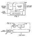
- Figure 1 shows components implemented on a single integrated circuit device or chip.
- a multiplexor 2 receives input data at a normal clock rate, for example 25MHz. The incoming data latched by a low rate clock signal, is multiplexed into a high rate data stream to be passed to a high speed device 4, for example a graphics processing device. Operation of the multiplexor 2 and the high speed device 4 is controlled in accordance with the principle of the present invention by an on chip clock accelerator 6 which receives the low rate clock signal and generates therefrom a high rate clock signal CLK synchronised with the low rate clock.
- the signal CLK comprises two signals in antiphase, CLK1 and CLK2.
- the basic construction of the clock accelerator is described with reference to Figure 2. It comprises an input circuit 8 for receiving the low rate clock signal and a plurality of sequentially connected delay devices which are represented in Figure 2 by the single box 10 connected to the input circuit 8.
- the output of the sequentially connected delay devices 10 is fed to an error generator 12 which also receives the low rate clock signal from the input circuit 8.
- the output signal from the error generator 12 is an error signal E which is fed to a loop filter 14 which integrates it to provide a common control voltage Vc for controlling the plurality of delay devices 10. Operation of the circuit will become clearer as each individual component is described in the following.
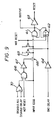
- the first delay device D0 is connected to receive the input clock signal from the input circuit 8.
- the next delay device D1 and subsequent delay devices D2 to D5 are connected in sequence to the first delay device D0.
- Each delay device acts to generate an output signal at a predetermined time interval after the receipt of a trigger signal.
- the output signal of each delay device D0 to D5 is received by an output means in the form of a buffer 16 which generates two antiphase clock signals in a manner to be described hereinafter.
- the detailed operation of the delay devices will also be described in more detail below.
- the input signal for the first delay device acts as a trigger signal to cause the first delay device to produce a trigger signal after a predetermined time interval t, in the form of a falling edge.
- the falling edge triggers the next delay device D1 which acts similarly to produce an output signal after time t.
- the output signal of each delay device is the inverse of its output trigger signal. This is repeated to the last delay device D5.
- the time intervals t are controlled by a common voltage signal Vc from the filter 14.
- the trigger signal output by the last delay device D5 is compared with the next incoming clock pulse, and any phase error E will influence the filter to alter the control voltage Vc and hence the time intervals. In this way, a series of pulses synchronised to the incoming clock signal and of equal length can be produced.
- time interval, t is the same for each delay device, achieved by supplying a common control signal, voltage Vc, to all the delay devices. This is the basis of clock signal production to be described later.
- the buffer 16 comprises a plurality of generation units, a generation unit being associated with each respective delay device Do to D5.
- each generation unit G0 to G5 is connected to drive two common output lines 18, 20 (see Figure 5).
- the output lines 18, 20 feed a driving unit 22 from whence issue the antiphase clock signals CLK1, CLK2 on respective ones of the output lines 18, 20.
- Each generation unit G0 to G5 is also connected to examine the output signal CLK1.
- two delay devices D4, D5 are shown with their respective associated generation units G4, G5.
- the circuit of Figure 3 has six delay devices. However, it may be desirable to utilise only four or five of these, depending on the required acceleration factor of the clock signal. This is indicated diagrammatically by the dotted arrows in Figure 3.
- each generation unit is connected to receive the output signal of its associated delay device and to drive appropriate signals onto the common output lines 18, 20.
- Each generation unit has three states: a neutral state in which the output signal CLK1 is examined; a first drive state in which a negative going pulse is driven onto one of the output lines and a positive going pulse is simultaneously driven onto the other output line; and a second drive state in which the pulses are reversed.
- the second clock signals are generated in the output lines as follows: prior to receipt of a trigger signal by its associated delay device a generation unit is in its neutral state examining CLK1. When a delay device receives a trigger signal the generation unit associated with that delay device responds to the output signal of that delay device to adopt one of its first and second drive states in dependence on the state of CLK1 just prior to the change of state of that generation unit. The length of each pulse is determined by the time interval t, of the delay devices.
- each generation unit The circuitry of each generation unit is shown in Figure 6.
- An input n-channel transistor 24 is connected to receive at its gate the output signal of the delay device associated with the generation unit. The output signal is also fed to a first inverter 26 and to the gates of p-channel transistors 28, 30. The output of the first inverter 26 is connected to the gates of n-channel transistors 32, 34.
- Each p-channel transistor 28, 30 forms with a respective n-channel transistor 32, 34 a transmission gate.
- a p-channel transistor 36 is connected between a voltage supply and the drain of the input transistor 24, the gate of this transistor 36 being fed from the output signal of a second inverter 38 connected to the drain of the input transistor 24.
- the second inverter 38 feeds a third inverter 40 which in turn feeds a fourth inverter 42.
- the input of the transmission gate 30, 34 is connected to the output of the third inverter 40 and the input of the transmission gate 28, 32 is connected to the output of the fourth inverter 42.
- the output of the transmission gate 30, 34 is connected to one of the output lines 18 and the output of the transmission gate 28, 32 is connected to the other of the output lines 20.
- the source of the input transistor 24 is connected to examine one of the output signals CLK1.
- the starting state is such that the clock signal CLK1 is high, its counterpart CLK2 is low and the delay device associated with the particular generation unit it is inactive; in other words, the signal applied to the input transistor 24 is high.
- the input transistor 24 is "on", its drain (the input of inverter 38) follows the clock signal CLK1 and goes high, the output of the inverter 38 hence goes low, the output of the inverter 40 goes high and the output of the inverter 42 goes low. Due to the inverter 26, the transistors 32 and 34 are however "off".
- the delay device associated with the generation unit becomes active and issues its output signal, which is the inverse of the falling edge trigger signal as described earlier, the input transistor 24 is turned “off” while the transistors 32 and 34 are turned “on”. That is, the signals at the outputs of the inverters 40 and 42 are connected respectively to the output lines 18 and 20. As discussed above, the output of the inverter 40 is high and the output of the inverter 42 is low. Hence, the clock signal CLK1 goes low and its counterpart CLK2 goes high, i.e. the reverse of the states prior to the delay device going active. It is a particular advantage of this invention that two antiphase and perfectly synchronised clock signals are produced without any additional circuitry. That is, it is as easy to produce two antiphase clock signals as it is to produce one. These clock signals and their relationship to the signals produced by the delay devices are shown in Figure 4.
- any suitable delay device such as a conventional monostable
- MOSFET metal oxide semiconductor field effect transistor
- Such techniques inherently involve exponential responses to the applied control signal with the result that the gain of the circuit is far too high under some operational conditions. This can be seen clearly in Figure 7 where the graph (i) shows the delay/control characteristic for a typical monostable. In contrast, the graph (ii) shows the desirable delay/control characteristic, that is with a fixed gain.
- the delay device has a timing circuit comprising a switch element in the form of an n-channel FET 50, a capacitor 52 connected to the drain of the transistor 50 and a comparator 54 having one input connected to receive the voltage developed across the capacitor 52 and the other input connected to receive the control voltage Vc.
- a constant current source (not shown) provides a fixed current Ic to the drain of the transistor 50.
- the delay device also includes a control circuit illustrated in Figure 8 only by box 56, which is arranged to receive the trigger signal (inputEdge) for the delay device (the falling edge issued by the preceding delay device) and to produce an output signal which is fed to the associated generation unit.
- the control signal circuit also produces a reset signal for the transistor 50 and receives the output signal (endDelay) of the comparator 54.
- the constant current Ic charges the capacitor 52 so that the voltage across the capacitor 52 increases linearly with time.
- the output of the comparator 54 will switch from low to high. It is an important feature of this arrangement that by using a fixed charging current, the increase in capacitor voltage with time will be as linear as the current is constant.
- the availability of a constant current serves to ensure the required linear delay response to the control voltage Vc.
- the low to high transition (endDelay) of the comparator 54 is fed to the control circuit 56 to produce the required output signals as will now be described.
- control circuit 56 Details of the control circuit 56 are shown in Figure 9.
- the control circuit is such that once it has become active it is insensitive to changes of its trigger signal but responds only to the endDelay signal from the comparator 54. Moreover, once the delay device has completed its timing operation and its output has once again gone low, it must not be immediately triggered by its input if that has remained low and not yet gone high.
- the control circuit comprises an FET transistor 58, the drain of which is coupled to receive the inputEdge signal for the delay device. The drain of the transistor is coupled to its gate by a NAND gate 66 sequentially connected to an inverter 67.
- the endDelay signal from the comparator 54 is fed to an inverter 64.
- the output of the inverter 64 is connected to the gate of a p-channel FET 65, the source of which is connected to one input of a NAND gate 61.
- This NAND gate 61 is cross-coupled with a second NAND gate 62 to form a flip-flop.
- the free input of the NAND gate 62 receives the output of the inverter 64.
- the output of the NAND gate 61 is inverted by an inverter 63 to provide the reset output for the transistor 50.
- the output of the NAND gate 61 is the output signal of the control circuit which serves to trigger the subsequent delay device.
- Setup circuitry in the form of a NOR gate 70 connected to one input of the NAND gate 66 is present to set the starting-up characteristics of the control circuit.
- the NAND gate 66, inverter 67 and transistor 58 constitute an edge detector.
- the transistor 58 serves as a PASS gate to transfer the low signal onto the input of the NAND gate 61 before it is turned off by the output of the inverter 67 acting on its gate.
- the output signal goes high and the reset signal goes low.
- the endDelay signal is low, as should be the case, then both the inputs to the NAND gate 62 are high ensuring that its output is low so keeping the NAND gate 61 in the set state.
- the endDelay signal goes high, the flip-flop comprising the NAND gate 61 and 62 will change state because both inputs to the NAND gate 61 will go high. In that situation, the output signal goes low and the reset signal goes high.
Abstract
Description
- This invention relates to clock generation and particularly to the generation of a clock signal on an integrated circuit.
- There have been recently dramatic increases in the performance of integrated circuit graphic systems, resulting in the requirement for ever increasing data rates. Data rates in mainstream graphics workstations have increased from 25MHz to over 100MHz, and future increases are probable.
- Currently, information destined for screen output is stored in a block of memory called a frame store which periodically outputs its information in a serial fashion at a rate called the pixel dot rate. This serial information can be manipulated by graphics hardware at the pixel dot rate and is ultimately converted by a digital-to-analogue converter (DAC) to analogue voltages which can control the electron guns in a cathode ray tube (CRT).
- To utilise readily available and cheap memory technology which cannot operate at such high speeds, the aforementioned frame store is split up into a plurality of smaller frame stores which operate more slowly and in parallel. Pixel data from the frame stores is outputted in parallel streams down a pipeline. These pixel streams are combined by a multiplexor into one high speed serial stream, upstream of the DAC.
- Generally such combination involves a high speed clock to control this multiplexor. Any graphics hardware required to operate on the high speed serial pixel stream will also have to be controlled by this high speed clock. It is known to provide the multiplexor combining the multiple pixel stream on the same silicon chip as a high speed sequential graphics device even though an external high speed clock at the pixel dot rate frequency has also had to be supplied to control both. This produces a synchronisation problem which is difficult to solve, because the low rate data entering the graphics device is not correlated with the high speed clock. Even if the low rate data is controlled by a signal derived from the high speed clock, for example by using a frequency divider, delays are such that at these high frequencies this has to be viewed as uncorrelated. In addition to this problem extra costs are incurred to generate the high speed clock.
- More generally, it is often required to take into a silicon chip several data streams at lower frequencies. Once combined into a single stream this data can be used as the input to another part of the chip. Both stages require the input of an external clock which is at the highest frequency that occurs on the chip. This is expensive and produces synchronisation problems.
- It is an object of the present invention to solve the problem of synchronising incoming data at a low rate with an integrated circuit processing device utilising that data at a higher rate.
- According to one aspect of the present invention there is provided an integrated circuit comprising: a multiplexor connected to receive incoming data at a first rate and controllable by a high rate clock signal to output that data serially at a second, higher rate; a processing device coupled to receive data output from the multiplexor at the higher rate and controllable by a high rate clock signal to process that data; and clock generation circuitry connected to receive a first clock signal at said first rate and operable to produce therefrom said high rate clock signal to be supplied to the processing device and to the multiplexor.
- By utilising clock generation circuitry which is part of the integrated circuit device to produce the high rate clock signal from the first clock signal used to regulate the incoming data it is possible to ensure that the operation of the processing device will be synchronised to the data rate of the data which it is processing.
- Thus, this invention relates in its preferred embodiment to the provision on chip of a multiplexor to take in slower parallel streams, a higher speed processing device, and a clock acceleration circuit to take in an input of a lower frequency and generate the required high frequency clock to control the rest of the chip. To ensure synchronisation, the lower frequency input used is the same frequency used to control the incoming data streams. Hence no such high frequency is now required to be supplied from an external source. Because all high frequency signals only exist within the bounds of this one chip (with the exception of the output which only goes straight to a CRT) then all timing and synchronisation problems can be solved by the chip designer, not the system designer.
- A user of the integrated circuits which will be sold in the form of a chip, need only provide a single, low rate clock and does not need to concern himself with the clock speed and synchronisation in the integrated circuit. This offers considerable attraction to purchasers of integrated circuit chips.
- According to another aspect of the present invention there is provided clock generation circuitry for providing from a first clock signal a second clock signal at a different rate, the circuitry comprising: a plurality of sequentially connected delay devices, a first one of which is coupled to receive the first clock signal, each delay device being operable to produce a trigger signal and an output signal at a predetermined time interval after receiving a trigger signal from the previously connected delay device; control means common to said delay devices for controlling said predetermined time interval; and output means coupled to receive the output signals of the delay devices to produce therefrom said second clock signal.
- It will be appreciated that the term clock signal is used to denote any periodic function and is not restrictive of the application to which such a function might be put.
- This clock generation circuitry is particularly suitable for use in the first aspect of the present invention, when the second clock signal is at a higher rate than the first clock signal.
- Preferably the control means is connected in a feedback loop so as to be responsive to an error signal resulting from comparison of the first clock signal with the output signal of the last connected delay device. By incorporating a control system in this way, the output signals of the connected delay devices can be made to occur in a regular fashion between consecutive pulses of the first clock signal.
- The output means can be arranged to provide two second clock signals at the same frequency but in antiphase.
- Circuitry of this type lends itself well to manufacture in an integrated circuit and obviates the need for an externally provided high rate clock signal. Effectively a first order control system has been created by replacing the voltage controlled oscillator of a phase locked loop with a triggered chain of events. This is easier to control yet stable over a large period of time and consequently more resistant to noise.
- The delay devices can be conventional delays or monostables of which numerous examples are known. A preferred delay device however is one devised by the present inventor and comprising a timing circuit and a control circuit, the timing circuit comprising a controllable switch element for receiving a reset signal, capacitive means connected to be charged up when said controllable switch element is in a first state, and comparator means connected to receive as a first input signal the voltage across the capacitive means, and as a second input signal a control voltage, and producing as an output a timing signal in dependence on said first and second input signals and the control circuit being connected to receive said timing signal and to provide in response thereto the trigger signal of the delay device and the said reset signal. The control voltage is conveniently derived from said control means of the clock generation circuitry.
- Such a monostable provides a greater dynamic range than known delay devices. This is usually limited in practice by the gain of a circuit being too high at some point in its characteristic, causing a sensitivity to noise under particular circumstances which is hard to suppress. Here this has been overcome by making the gain (expressed as the change in said predetermined time interval for a certain change in said control voltage), as constant as possible between the two end points of the required dynamic range. This ensures that the gain is no higher than it needs to be to achieve the required minimum and maximum time intervals. In the preferred embodiment this is achieved by not using, in contrast to conventional delay devices, a low biased MOSFET to limit any currents or to add loads to certain nodes to perform the control of the delay device.
- The number of selected delay devices affects the multiplication factor by which the second clock signal differs from the first clock signal. The clock generation circuitry can be manufactured with p delay devices with means for selecting n of the p delay devices (where n≦p) for use in generation of the second clock signal. In this way it is unnecessary to decide at the manufacturing stage how many delay devices are required for any specific application.
- Where the number p of delay devices is a known, even number, the output means for producing the second clock signals can be designed as a fixed logic array without too much difficulty. However, when an unknown number n of delay devices is to be utilised a more sophisticated arrangement is required. According to one embodiment of the present invention said output means comprises a plurality of generation units connected respectively to receive the output signals of the p delay devices, the generation units being individually connectable to a common output line and each generation unit having three states: a neutral state in which the output line is examined; a negative drive state in which a negative going pulse is driven onto the output line; and a positive drive state in which a positive going pulse is driven onto the output line, the second clock signal thereby being generated on the output line as follows: prior to receipt of a trigger signal by its associated delay device a generation unit is in its neutral state and when a delay device receives a trigger signal the generation unit associated with that delay device responds to the output signal of that delay device to adopt one of its positive and negative drive states in dependence on the state of the second clock signal just prior to the change of state of that generation unit.
- The generation units can also be individually connectable to a second common output line and arranged so that in their negative drive states a positive going pulse is driven onto the second common output line and in their positive drive states a negative going pulse is driven onto the second common output line thereby to generate a clock signal in antiphase to said second clock signal.
- For a better understanding of the present invention, and to show how the same can be carried into effect, reference will now be made, by way of example, to the accompanying drawings, in which:-
- Figure 1 is a schematic diagram showing the principle of on chip clock generation;
- Figure 2 is a schematic diagram showing the principle of an embodiment of the present invention using feedback;
- Figure 3 is a more detailed diagram of the embodiment of the present invention shown in Figure 2;
- Figure 4 is a timing diagram for the operation of the circuitry of Figure 3;
- Figure 5 is a schematic diagram of the generation units;
- Figure 6 is a circuit diagram of one generation unit;
- Figure 7 is a graph showing the relationship between change in time interval and changes in the control voltage for different delay devices;
- Figure 8 is a circuit diagram of a delay device in accordance with one embodiment of the invention; and
- Figure 9 is a circuit diagram of the control circuit of Figure 8.
- Figure 1 shows components implemented on a single integrated circuit device or chip. A
multiplexor 2 receives input data at a normal clock rate, for example 25MHz. The incoming data latched by a low rate clock signal, is multiplexed into a high rate data stream to be passed to a high speed device 4, for example a graphics processing device. Operation of themultiplexor 2 and the high speed device 4 is controlled in accordance with the principle of the present invention by an onchip clock accelerator 6 which receives the low rate clock signal and generates therefrom a high rate clock signal CLK synchronised with the low rate clock. The signal CLK comprises two signals in antiphase, CLK1 and CLK2. - The basic construction of the clock accelerator is described with reference to Figure 2. It comprises an input circuit 8 for receiving the low rate clock signal and a plurality of sequentially connected delay devices which are represented in Figure 2 by the
single box 10 connected to the input circuit 8. The output of the sequentiallyconnected delay devices 10 is fed to anerror generator 12 which also receives the low rate clock signal from the input circuit 8. The output signal from theerror generator 12 is an error signal E which is fed to aloop filter 14 which integrates it to provide a common control voltage Vc for controlling the plurality ofdelay devices 10. Operation of the circuit will become clearer as each individual component is described in the following. - Referring now to Figure 3 the plurality of delay devices Do to D5 in the
box 10 are shown individually. The first delay device D0 is connected to receive the input clock signal from the input circuit 8. The next delay device D1 and subsequent delay devices D2 to D5 are connected in sequence to the first delay device D0. Each delay device acts to generate an output signal at a predetermined time interval after the receipt of a trigger signal. The output signal of each delay device D0 to D5 is received by an output means in the form of a buffer 16 which generates two antiphase clock signals in a manner to be described hereinafter. The detailed operation of the delay devices will also be described in more detail below. However, referring to Figure 4, it is noted here that the input signal for the first delay device acts as a trigger signal to cause the first delay device to produce a trigger signal after a predetermined time interval t, in the form of a falling edge. The falling edge triggers the next delay device D1 which acts similarly to produce an output signal after time t. As will become clearer in the following, in the described embodiment the output signal of each delay device is the inverse of its output trigger signal. This is repeated to the last delay device D5. The time intervals t, are controlled by a common voltage signal Vc from thefilter 14. The trigger signal output by the last delay device D5 is compared with the next incoming clock pulse, and any phase error E will influence the filter to alter the control voltage Vc and hence the time intervals. In this way, a series of pulses synchronised to the incoming clock signal and of equal length can be produced. - It is important to note that the time interval, t, is the same for each delay device, achieved by supplying a common control signal, voltage Vc, to all the delay devices. This is the basis of clock signal production to be described later.
- The buffer 16 comprises a plurality of generation units, a generation unit being associated with each respective delay device Do to D5. In the buffer each generation unit G0 to G5 is connected to drive two
common output lines 18, 20 (see Figure 5). The output lines 18, 20 feed a driving unit 22 from whence issue the antiphase clock signals CLK1, CLK2 on respective ones of theoutput lines 18, 20. Each generation unit G0 to G5 is also connected to examine the output signal CLK1. In Figure 5, two delay devices D4, D5 are shown with their respective associated generation units G4, G5. - The circuit of Figure 3 has six delay devices. However, it may be desirable to utilise only four or five of these, depending on the required acceleration factor of the clock signal. This is indicated diagrammatically by the dotted arrows in Figure 3.
- Where the number of delay devices is a known, even number, the output means 16 for producing the second clock signal could be designed as a fixed logic array without too much difficulty. However, when an unknown number of delay devices is to be selected, a more sophisticated arrangement is required, utilising the generation units discussed above. Each generation unit is connected to receive the output signal of its associated delay device and to drive appropriate signals onto the
common output lines 18, 20. Each generation unit has three states: a neutral state in which the output signal CLK1 is examined; a first drive state in which a negative going pulse is driven onto one of the output lines and a positive going pulse is simultaneously driven onto the other output line; and a second drive state in which the pulses are reversed. The second clock signals are generated in the output lines as follows: prior to receipt of a trigger signal by its associated delay device a generation unit is in its neutral state examining CLK1. When a delay device receives a trigger signal the generation unit associated with that delay device responds to the output signal of that delay device to adopt one of its first and second drive states in dependence on the state of CLK1 just prior to the change of state of that generation unit. The length of each pulse is determined by the time interval t, of the delay devices. - The circuitry of each generation unit is shown in Figure 6. An input n-
channel transistor 24 is connected to receive at its gate the output signal of the delay device associated with the generation unit. The output signal is also fed to afirst inverter 26 and to the gates of p-channel transistors 28, 30. The output of thefirst inverter 26 is connected to the gates of n-channel transistors channel transistor 28, 30 forms with a respective n-channel transistor 32, 34 a transmission gate. A p-channel transistor 36 is connected between a voltage supply and the drain of theinput transistor 24, the gate of thistransistor 36 being fed from the output signal of asecond inverter 38 connected to the drain of theinput transistor 24. Thesecond inverter 38 feeds athird inverter 40 which in turn feeds afourth inverter 42. The input of thetransmission gate 30, 34 is connected to the output of thethird inverter 40 and the input of thetransmission gate fourth inverter 42. The output of thetransmission gate 30, 34 is connected to one of theoutput lines 18 and the output of thetransmission gate input transistor 24 is connected to examine one of the output signals CLK1. - It will be assumed for the purposes of the following explanation that the starting state is such that the clock signal CLK1 is high, its counterpart CLK2 is low and the delay device associated with the particular generation unit it is inactive; in other words, the signal applied to the
input transistor 24 is high. In these circumstances, theinput transistor 24 is "on", its drain (the input of inverter 38) follows the clock signal CLK1 and goes high, the output of theinverter 38 hence goes low, the output of theinverter 40 goes high and the output of theinverter 42 goes low. Due to theinverter 26, thetransistors input transistor 24 is turned "off" while thetransistors inverters output lines 18 and 20. As discussed above, the output of theinverter 40 is high and the output of theinverter 42 is low. Hence, the clock signal CLK1 goes low and its counterpart CLK2 goes high, i.e. the reverse of the states prior to the delay device going active. It is a particular advantage of this invention that two antiphase and perfectly synchronised clock signals are produced without any additional circuitry. That is, it is as easy to produce two antiphase clock signals as it is to produce one. These clock signals and their relationship to the signals produced by the delay devices are shown in Figure 4. - The individual delay devices will now be described. Although in principle any suitable delay device, such as a conventional monostable, could be used in the circuit of the present invention, such monostables generally rely on a low biased MOSFET (metal oxide semiconductor field effect transistor) to limit currents or add loads to certain nodes to perform the control of the monostables. Such techniques inherently involve exponential responses to the applied control signal with the result that the gain of the circuit is far too high under some operational conditions. This can be seen clearly in Figure 7 where the graph (i) shows the delay/control characteristic for a typical monostable. In contrast, the graph (ii) shows the desirable delay/control characteristic, that is with a fixed gain. Although to the right hand side of the dotted line, the characteristic curve (i) is satisfactory, to the left of that line it is undesirable since it requires an extremely stable control for its operation. The characteristic curve (ii) is more tolerant of control conditions. One way of achieving a delay device which conforms more closely to the characteristic curve (ii) is shown in Figure 8. The delay device has a timing circuit comprising a switch element in the form of an n-channel FET 50, a
capacitor 52 connected to the drain of the transistor 50 and acomparator 54 having one input connected to receive the voltage developed across thecapacitor 52 and the other input connected to receive the control voltage Vc. A constant current source (not shown) provides a fixed current Ic to the drain of the transistor 50. The delay device also includes a control circuit illustrated in Figure 8 only bybox 56, which is arranged to receive the trigger signal (inputEdge) for the delay device (the falling edge issued by the preceding delay device) and to produce an output signal which is fed to the associated generation unit. The control signal circuit also produces a reset signal for the transistor 50 and receives the output signal (endDelay) of thecomparator 54. With the transistor 50 in the "off" state, the constant current Ic charges thecapacitor 52 so that the voltage across thecapacitor 52 increases linearly with time. As the voltage across the capacitor exceeds the control voltage Vc, the output of thecomparator 54 will switch from low to high. It is an important feature of this arrangement that by using a fixed charging current, the increase in capacitor voltage with time will be as linear as the current is constant. The availability of a constant current serves to ensure the required linear delay response to the control voltage Vc. The low to high transition (endDelay) of thecomparator 54 is fed to thecontrol circuit 56 to produce the required output signals as will now be described. - Details of the
control circuit 56 are shown in Figure 9. The control circuit is such that once it has become active it is insensitive to changes of its trigger signal but responds only to the endDelay signal from thecomparator 54. Moreover, once the delay device has completed its timing operation and its output has once again gone low, it must not be immediately triggered by its input if that has remained low and not yet gone high. The control circuit comprises anFET transistor 58, the drain of which is coupled to receive the inputEdge signal for the delay device. The drain of the transistor is coupled to its gate by aNAND gate 66 sequentially connected to aninverter 67. The endDelay signal from thecomparator 54 is fed to aninverter 64. The output of theinverter 64 is connected to the gate of a p-channel FET 65, the source of which is connected to one input of aNAND gate 61. ThisNAND gate 61 is cross-coupled with a second NAND gate 62 to form a flip-flop. The free input of the NAND gate 62 receives the output of theinverter 64. The output of theNAND gate 61 is inverted by aninverter 63 to provide the reset output for the transistor 50. The output of theNAND gate 61 is the output signal of the control circuit which serves to trigger the subsequent delay device. Setup circuitry in the form of a NORgate 70 connected to one input of theNAND gate 66 is present to set the starting-up characteristics of the control circuit. - Assuming that the inputEdge signal is initially high and goes low, the
NAND gate 66,inverter 67 andtransistor 58 constitute an edge detector. Thetransistor 58 serves as a PASS gate to transfer the low signal onto the input of theNAND gate 61 before it is turned off by the output of theinverter 67 acting on its gate. As a result of the input of theNAND gate 61 going low, the output signal goes high and the reset signal goes low. If the endDelay signal is low, as should be the case, then both the inputs to the NAND gate 62 are high ensuring that its output is low so keeping theNAND gate 61 in the set state. When the endDelay signal goes high, the flip-flop comprising theNAND gate 61 and 62 will change state because both inputs to theNAND gate 61 will go high. In that situation, the output signal goes low and the reset signal goes high.
Claims (9)
Priority Applications (1)
| Application Number | Priority Date | Filing Date | Title |
|---|---|---|---|
| EP97201653A EP0803791B1 (en) | 1989-07-07 | 1990-06-26 | Clock Generation |
Applications Claiming Priority (2)
| Application Number | Priority Date | Filing Date | Title |
|---|---|---|---|
| GB8915583 | 1989-07-07 | ||
| GB8915583A GB2234371A (en) | 1989-07-07 | 1989-07-07 | Clock generation |
Related Child Applications (1)
| Application Number | Title | Priority Date | Filing Date |
|---|---|---|---|
| EP97201653.9 Division-Into | 1997-06-02 |
Publications (3)
| Publication Number | Publication Date |
|---|---|
| EP0407082A2 true EP0407082A2 (en) | 1991-01-09 |
| EP0407082A3 EP0407082A3 (en) | 1994-05-25 |
| EP0407082B1 EP0407082B1 (en) | 1997-12-10 |
Family
ID=10659683
Family Applications (2)
| Application Number | Title | Priority Date | Filing Date |
|---|---|---|---|
| EP97201653A Expired - Lifetime EP0803791B1 (en) | 1989-07-07 | 1990-06-26 | Clock Generation |
| EP90306976A Expired - Lifetime EP0407082B1 (en) | 1989-07-07 | 1990-06-26 | Clock generation |
Family Applications Before (1)
| Application Number | Title | Priority Date | Filing Date |
|---|---|---|---|
| EP97201653A Expired - Lifetime EP0803791B1 (en) | 1989-07-07 | 1990-06-26 | Clock Generation |
Country Status (5)
| Country | Link |
|---|---|
| US (3) | US5243597A (en) |
| EP (2) | EP0803791B1 (en) |
| JP (1) | JP2944713B2 (en) |
| DE (2) | DE69033309T2 (en) |
| GB (1) | GB2234371A (en) |
Cited By (1)
| Publication number | Priority date | Publication date | Assignee | Title |
|---|---|---|---|---|
| WO1994026028A1 (en) * | 1993-04-30 | 1994-11-10 | Inmos Limited | Frequency doubler |
Families Citing this family (45)
| Publication number | Priority date | Publication date | Assignee | Title |
|---|---|---|---|---|
| US5481573A (en) * | 1992-06-26 | 1996-01-02 | International Business Machines Corporation | Synchronous clock distribution system |
| FR2710800B1 (en) * | 1993-09-27 | 1995-12-15 | Sgs Thomson Microelectronics | Digital delay line. |
| JP3232351B2 (en) * | 1993-10-06 | 2001-11-26 | 三菱電機株式会社 | Digital circuit device |
| US6009039A (en) * | 1994-02-17 | 1999-12-28 | Fujitsu Limited | Semiconductor device |
| KR0158762B1 (en) * | 1994-02-17 | 1998-12-01 | 세키자와 다다시 | Semiconductor device |
| US5451911A (en) * | 1994-04-07 | 1995-09-19 | Media Vision, Inc. | Timing generator |
| US5666079A (en) * | 1994-05-06 | 1997-09-09 | Plx Technology, Inc. | Binary relative delay line |
| US5586308A (en) * | 1994-10-19 | 1996-12-17 | Advanced Micro Devices, Inc. | Clock control unit responsive to a power management state for clocking multiple clocked circuits connected thereto |
| US5572719A (en) * | 1994-11-22 | 1996-11-05 | Advanced Micro Devices | Clock control system for microprocessors including a delay sensing circuit |
| JPH0951254A (en) * | 1995-08-03 | 1997-02-18 | Mitsubishi Electric Corp | Clock generator |
| JPH0955667A (en) * | 1995-08-10 | 1997-02-25 | Mitsubishi Electric Corp | Multiplexer and demultiplexer |
| US5691660A (en) * | 1995-11-28 | 1997-11-25 | International Business Machines Corporation | Clock synchronization scheme for fractional multiplication systems |
| JP3125682B2 (en) * | 1996-06-21 | 2001-01-22 | 日本電気株式会社 | Clock supply system and clock supply system |
| US5719445A (en) * | 1996-12-23 | 1998-02-17 | Sgs-Thomson Microelectronics, Inc. | Input delay control |
| US5933035A (en) * | 1996-12-31 | 1999-08-03 | Cirrus Logic, Inc. | Digital clock frequency multiplication circuit and method |
| US5978379A (en) | 1997-01-23 | 1999-11-02 | Gadzoox Networks, Inc. | Fiber channel learning bridge, learning half bridge, and protocol |
| JP3500026B2 (en) * | 1997-01-27 | 2004-02-23 | 矢崎総業株式会社 | Data modulation device and data modulation method |
| JP3500028B2 (en) * | 1997-01-29 | 2004-02-23 | 矢崎総業株式会社 | Data demodulation device and data demodulation method |
| JPH11163690A (en) * | 1997-11-26 | 1999-06-18 | Toshiba Corp | Frequency multiplication circuit |
| US6175928B1 (en) * | 1997-12-31 | 2001-01-16 | Intel Corporation | Reducing timing variance of signals from an electronic device |
| US6148199A (en) * | 1998-01-30 | 2000-11-14 | Motorola, Inc. | Apparatus and method of updating a mobility database |
| US6057791A (en) * | 1998-02-18 | 2000-05-02 | Oasis Design, Inc. | Apparatus and method for clocking digital and analog circuits on a common substrate to enhance digital operation and reduce analog sampling error |
| US7430171B2 (en) | 1998-11-19 | 2008-09-30 | Broadcom Corporation | Fibre channel arbitrated loop bufferless switch circuitry to increase bandwidth without significant increase in cost |
| CA2263061C (en) * | 1999-02-26 | 2011-01-25 | Ki-Jun Lee | Dual control analog delay element |
| US6911855B2 (en) | 1999-06-28 | 2005-06-28 | Broadcom Corporation | Current-controlled CMOS circuit using higher voltage supply in low voltage CMOS process |
| US6897697B2 (en) * | 1999-06-28 | 2005-05-24 | Broadcom Corporation | Current-controlled CMOS circuit using higher voltage supply in low voltage CMOS process |
| US6424194B1 (en) | 1999-06-28 | 2002-07-23 | Broadcom Corporation | Current-controlled CMOS logic family |
| US6340899B1 (en) | 2000-02-24 | 2002-01-22 | Broadcom Corporation | Current-controlled CMOS circuits with inductive broadbanding |
| GB2363498B (en) * | 2000-06-16 | 2005-06-01 | Marconi Caswell Ltd | Transponder device for generating a data bearing output |
| US6826399B1 (en) | 2000-06-30 | 2004-11-30 | Motorola, Inc. | Apparatus and method of updating a mobility database |
| US6864558B2 (en) | 2001-05-17 | 2005-03-08 | Broadcom Corporation | Layout technique for C3MOS inductive broadbanding |
| US20040232954A1 (en) * | 2001-07-06 | 2004-11-25 | Van Zeijl Paulus Thomas | Signal generator device, method for generating a signal and devices including such a signal generator device |
| US7239636B2 (en) * | 2001-07-23 | 2007-07-03 | Broadcom Corporation | Multiple virtual channels for use in network devices |
| US6791380B2 (en) * | 2001-11-27 | 2004-09-14 | Winbond Electronics Corporation | Universal clock generator |
| US7295555B2 (en) | 2002-03-08 | 2007-11-13 | Broadcom Corporation | System and method for identifying upper layer protocol message boundaries |
| US7411959B2 (en) * | 2002-08-30 | 2008-08-12 | Broadcom Corporation | System and method for handling out-of-order frames |
| US7934021B2 (en) | 2002-08-29 | 2011-04-26 | Broadcom Corporation | System and method for network interfacing |
| US7346701B2 (en) | 2002-08-30 | 2008-03-18 | Broadcom Corporation | System and method for TCP offload |
| US8180928B2 (en) | 2002-08-30 | 2012-05-15 | Broadcom Corporation | Method and system for supporting read operations with CRC for iSCSI and iSCSI chimney |
| US7313623B2 (en) | 2002-08-30 | 2007-12-25 | Broadcom Corporation | System and method for TCP/IP offload independent of bandwidth delay product |
| US7598811B2 (en) | 2005-07-29 | 2009-10-06 | Broadcom Corporation | Current-controlled CMOS (C3MOS) fully differential integrated wideband amplifier/equalizer with adjustable gain and frequency response without additional power or loading |
| US7362174B2 (en) | 2005-07-29 | 2008-04-22 | Broadcom Corporation | Current-controlled CMOS (C3MOS) wideband input data amplifier for reduced differential and common-mode reflection |
| US7598788B2 (en) | 2005-09-06 | 2009-10-06 | Broadcom Corporation | Current-controlled CMOS (C3MOS) fully differential integrated delay cell with variable delay and high bandwidth |
| JP4772801B2 (en) | 2005-12-20 | 2011-09-14 | 株式会社アドバンテスト | Oscillation circuit, test apparatus, and electronic device |
| US9460814B2 (en) | 2014-05-02 | 2016-10-04 | Globalfoundries Inc. | Memory tester design for soft error rate (SER) failure analysis |
Citations (3)
| Publication number | Priority date | Publication date | Assignee | Title |
|---|---|---|---|---|
| US3631464A (en) * | 1969-03-21 | 1971-12-28 | Singer General Precision | Digital parallel to serial converter |
| EP0274606A2 (en) * | 1986-11-21 | 1988-07-20 | Siemens Aktiengesellschaft | Arrangement for creating an integrated CMOS ciruit technique delay network and a phase comparator section |
| EP0346896A2 (en) * | 1988-06-16 | 1989-12-20 | Fujitsu Limited | A parallel-to-serial converter |
Family Cites Families (9)
| Publication number | Priority date | Publication date | Assignee | Title |
|---|---|---|---|---|
| US3995119A (en) * | 1975-05-30 | 1976-11-30 | Gte Automatic Electric Laboratories Incorporated | Digital time-division multiplexing system |
| US4316148A (en) * | 1979-09-04 | 1982-02-16 | Sperry Corporation | Variable frequency logic clock |
| JPS6089773A (en) * | 1983-08-01 | 1985-05-20 | フエアチアイルド カメラ アンド インストルメント コ−ポレ−シヨン | Method and device for dynamically controlling timing of signal in automatic test system |
| NL8303561A (en) * | 1983-10-17 | 1985-05-17 | Philips Nv | REGULATED OSCILLATOR SHIFT. |
| WO1985002275A1 (en) * | 1983-11-07 | 1985-05-23 | Motorola, Inc. | Synthesized clock microcomputer with power saving |
| US4613775A (en) * | 1984-06-08 | 1986-09-23 | International Business Machines Corporation | Apparatus or method for stabilizing the frequency of a clock signal generated from an on-chip clock generator |
| US4658161A (en) * | 1985-08-13 | 1987-04-14 | Hewlett-Packard Company | Split phase loop |
| US4691124A (en) * | 1986-05-16 | 1987-09-01 | Motorola, Inc. | Self-compensating, maximum speed integrated circuit |
| US4899071A (en) * | 1988-08-02 | 1990-02-06 | Standard Microsystems Corporation | Active delay line circuit |
-
1989
- 1989-07-07 GB GB8915583A patent/GB2234371A/en not_active Withdrawn
-
1990
- 1990-06-22 US US07/542,320 patent/US5243597A/en not_active Expired - Lifetime
- 1990-06-26 EP EP97201653A patent/EP0803791B1/en not_active Expired - Lifetime
- 1990-06-26 DE DE69033309T patent/DE69033309T2/en not_active Expired - Fee Related
- 1990-06-26 DE DE69031788T patent/DE69031788T2/en not_active Expired - Fee Related
- 1990-06-26 EP EP90306976A patent/EP0407082B1/en not_active Expired - Lifetime
- 1990-07-06 JP JP2179424A patent/JP2944713B2/en not_active Expired - Lifetime
-
1992
- 1992-08-24 US US07/933,679 patent/US5389830A/en not_active Expired - Lifetime
-
1993
- 1993-02-25 US US08/023,201 patent/US5345449A/en not_active Expired - Lifetime
Patent Citations (3)
| Publication number | Priority date | Publication date | Assignee | Title |
|---|---|---|---|---|
| US3631464A (en) * | 1969-03-21 | 1971-12-28 | Singer General Precision | Digital parallel to serial converter |
| EP0274606A2 (en) * | 1986-11-21 | 1988-07-20 | Siemens Aktiengesellschaft | Arrangement for creating an integrated CMOS ciruit technique delay network and a phase comparator section |
| EP0346896A2 (en) * | 1988-06-16 | 1989-12-20 | Fujitsu Limited | A parallel-to-serial converter |
Non-Patent Citations (1)
| Title |
|---|
| IBM TECHNICAL DISCLOSURE BULLETIN. vol. 26, no. 3A , August 1983 , NEW YORK US pages 990 - 991 I. HERNANDEZ 'Frequency multiplier using delay circuits.' * |
Cited By (8)
| Publication number | Priority date | Publication date | Assignee | Title |
|---|---|---|---|---|
| WO1994026028A1 (en) * | 1993-04-30 | 1994-11-10 | Inmos Limited | Frequency doubler |
| US5525938A (en) * | 1993-04-30 | 1996-06-11 | Inmos Limited | Ring oscillator using current mirror inverter stages |
| EP0749207A2 (en) * | 1993-04-30 | 1996-12-18 | STMicroelectronics Limited | Frequency doubler |
| EP0749207A3 (en) * | 1993-04-30 | 1997-01-15 | STMicroelectronics Limited | Frequency doubler |
| US5602514A (en) * | 1993-04-30 | 1997-02-11 | Sgs-Thomson Microelectronics, Ltd. | Quadrature oscillator having a variable frequency |
| US5635866A (en) * | 1993-04-30 | 1997-06-03 | Sgs-Thomson Microelectronics Limited | Frequency Doubler |
| US5635877A (en) * | 1993-04-30 | 1997-06-03 | Sgs-Thomson Microelectronics Ltd. | Low voltage high frequency ring oscillator for controling phase-shifted outputs |
| USRE37124E1 (en) | 1993-04-30 | 2001-04-03 | Stmicroelectronics Limited | Ring oscillator using current mirror inverter stages |
Also Published As
| Publication number | Publication date |
|---|---|
| US5389830A (en) | 1995-02-14 |
| US5345449A (en) | 1994-09-06 |
| EP0803791A1 (en) | 1997-10-29 |
| DE69031788T2 (en) | 1998-07-09 |
| JP2944713B2 (en) | 1999-09-06 |
| US5243597A (en) | 1993-09-07 |
| EP0407082A3 (en) | 1994-05-25 |
| EP0803791B1 (en) | 1999-09-29 |
| DE69033309T2 (en) | 2000-02-24 |
| EP0407082B1 (en) | 1997-12-10 |
| GB2234371A (en) | 1991-01-30 |
| GB8915583D0 (en) | 1989-08-23 |
| DE69031788D1 (en) | 1998-01-22 |
| DE69033309D1 (en) | 1999-11-04 |
| JPH0357008A (en) | 1991-03-12 |
Similar Documents
| Publication | Publication Date | Title |
|---|---|---|
| US5243597A (en) | Clock generation | |
| US5497263A (en) | Variable delay circuit and clock signal supply unit using the same | |
| KR100303804B1 (en) | Clock delay circuitry, and oscillation circuitry and phase synchronization circuitry using the clock delay circuitry | |
| KR100325188B1 (en) | Digital phase locked loop capable of suppressing jitter | |
| US5619170A (en) | PLL timing generator with voltage controlled oscillator | |
| USRE37232E1 (en) | Delay circuit device | |
| US6194950B1 (en) | High-speed CMOS multiplexer | |
| US5898242A (en) | Self-calibrating clock circuit employing a continuously variable delay module in a feedback loop | |
| US4356411A (en) | Flip-flop circuit | |
| US7151398B2 (en) | Clock signal generators having programmable full-period clock skew control | |
| US3993916A (en) | Functionally static type semiconductor shift register with half dynamic-half static stages | |
| KR100342896B1 (en) | Synchronous delay circuit | |
| JPH08506949A (en) | Signal processing circuit and method for delaying a binary periodic input signal | |
| US6313673B1 (en) | Frequency-dividing circuit capable of generating frequency-divided signal having duty ratio of 50% | |
| US6967512B2 (en) | Multiphase-clock processing circuit and clock multiplying circuit | |
| JPH10150350A (en) | Phase synchronization circuit and storage device using the phase synchronization circuit | |
| US5742550A (en) | Semiconductor integrated circuit device | |
| GB2255481A (en) | High speed bit-serial systems | |
| EP0610052A2 (en) | Method and apparatus for timing control | |
| EP0201128B1 (en) | Integrated electronic multiplex circuit and integrated electronic circuit including such a multiplex circuit | |
| JP2894040B2 (en) | Latch circuit | |
| US20050093576A1 (en) | Three-transistor nand and nor gates for two-phase clock generators | |
| US6753715B2 (en) | System for symmetric pulse generator flip-flop | |
| KR100278271B1 (en) | A clock frequency divider | |
| CN114665822A (en) | Oscillating circuit |
Legal Events
| Date | Code | Title | Description |
|---|---|---|---|
| PUAI | Public reference made under article 153(3) epc to a published international application that has entered the european phase |
Free format text: ORIGINAL CODE: 0009012 |
|
| AK | Designated contracting states |
Kind code of ref document: A2 Designated state(s): DE FR GB IT NL |
|
| 17P | Request for examination filed |
Effective date: 19901217 |
|
| PUAL | Search report despatched |
Free format text: ORIGINAL CODE: 0009013 |
|
| PUAF | Information related to the publication of a search report (a3 document) modified or deleted |
Free format text: ORIGINAL CODE: 0009199SEPU |
|
| AK | Designated contracting states |
Kind code of ref document: A3 Designated state(s): DE FR GB IT NL |
|
| D17D | Deferred search report published (deleted) | ||
| PUAL | Search report despatched |
Free format text: ORIGINAL CODE: 0009013 |
|
| AK | Designated contracting states |
Kind code of ref document: A3 Designated state(s): DE FR GB IT NL |
|
| RAP1 | Party data changed (applicant data changed or rights of an application transferred) |
Owner name: SGS-THOMSON MICROELECTRONICS LIMITED |
|
| 17Q | First examination report despatched |
Effective date: 19960112 |
|
| GRAG | Despatch of communication of intention to grant |
Free format text: ORIGINAL CODE: EPIDOS AGRA |
|
| GRAG | Despatch of communication of intention to grant |
Free format text: ORIGINAL CODE: EPIDOS AGRA |
|
| GRAH | Despatch of communication of intention to grant a patent |
Free format text: ORIGINAL CODE: EPIDOS IGRA |
|
| GRAH | Despatch of communication of intention to grant a patent |
Free format text: ORIGINAL CODE: EPIDOS IGRA |
|
| GRAA | (expected) grant |
Free format text: ORIGINAL CODE: 0009210 |
|
| AK | Designated contracting states |
Kind code of ref document: B1 Designated state(s): DE FR GB IT NL |
|
| DX | Miscellaneous (deleted) | ||
| PG25 | Lapsed in a contracting state [announced via postgrant information from national office to epo] |
Ref country code: NL Free format text: LAPSE BECAUSE OF FAILURE TO SUBMIT A TRANSLATION OF THE DESCRIPTION OR TO PAY THE FEE WITHIN THE PRESCRIBED TIME-LIMIT Effective date: 19971210 |
|
| REF | Corresponds to: |
Ref document number: 69031788 Country of ref document: DE Date of ref document: 19980122 |
|
| ITF | It: translation for a ep patent filed |
Owner name: PORTA CHECCACCI E BOTTI S.R.L. |
|
| ET | Fr: translation filed | ||
| NLV1 | Nl: lapsed or annulled due to failure to fulfill the requirements of art. 29p and 29m of the patents act | ||
| PLBE | No opposition filed within time limit |
Free format text: ORIGINAL CODE: 0009261 |
|
| STAA | Information on the status of an ep patent application or granted ep patent |
Free format text: STATUS: NO OPPOSITION FILED WITHIN TIME LIMIT |
|
| 26N | No opposition filed | ||
| REG | Reference to a national code |
Ref country code: FR Ref legal event code: D6 |
|
| PGFP | Annual fee paid to national office [announced via postgrant information from national office to epo] |
Ref country code: FR Payment date: 20000612 Year of fee payment: 11 |
|
| PGFP | Annual fee paid to national office [announced via postgrant information from national office to epo] |
Ref country code: GB Payment date: 20000621 Year of fee payment: 11 |
|
| PGFP | Annual fee paid to national office [announced via postgrant information from national office to epo] |
Ref country code: DE Payment date: 20000626 Year of fee payment: 11 |
|
| PG25 | Lapsed in a contracting state [announced via postgrant information from national office to epo] |
Ref country code: GB Free format text: LAPSE BECAUSE OF NON-PAYMENT OF DUE FEES Effective date: 20010626 |
|
| GBPC | Gb: european patent ceased through non-payment of renewal fee |
Effective date: 20010626 |
|
| PG25 | Lapsed in a contracting state [announced via postgrant information from national office to epo] |
Ref country code: FR Free format text: LAPSE BECAUSE OF NON-PAYMENT OF DUE FEES Effective date: 20020228 |
|
| PG25 | Lapsed in a contracting state [announced via postgrant information from national office to epo] |
Ref country code: DE Free format text: LAPSE BECAUSE OF NON-PAYMENT OF DUE FEES Effective date: 20020403 |
|
| PG25 | Lapsed in a contracting state [announced via postgrant information from national office to epo] |
Ref country code: IT Free format text: LAPSE BECAUSE OF NON-PAYMENT OF DUE FEES Effective date: 20050626 |