EP0402532B1 - Residue arithmetic apparatus - Google Patents
Residue arithmetic apparatus Download PDFInfo
- Publication number
- EP0402532B1 EP0402532B1 EP89201506A EP89201506A EP0402532B1 EP 0402532 B1 EP0402532 B1 EP 0402532B1 EP 89201506 A EP89201506 A EP 89201506A EP 89201506 A EP89201506 A EP 89201506A EP 0402532 B1 EP0402532 B1 EP 0402532B1
- Authority
- EP
- European Patent Office
- Prior art keywords
- input
- output
- circuit
- modulo
- representation
- Prior art date
- Legal status (The legal status is an assumption and is not a legal conclusion. Google has not performed a legal analysis and makes no representation as to the accuracy of the status listed.)
- Expired - Lifetime
Links
Images


Classifications
-
- G—PHYSICS
- G06—COMPUTING OR CALCULATING; COUNTING
- G06F—ELECTRIC DIGITAL DATA PROCESSING
- G06F7/00—Methods or arrangements for processing data by operating upon the order or content of the data handled
- G06F7/60—Methods or arrangements for performing computations using a digital non-denominational number representation, i.e. number representation without radix; Computing devices using combinations of denominational and non-denominational quantity representations, e.g. using difunction pulse trains, STEELE computers, phase computers
- G06F7/72—Methods or arrangements for performing computations using a digital non-denominational number representation, i.e. number representation without radix; Computing devices using combinations of denominational and non-denominational quantity representations, e.g. using difunction pulse trains, STEELE computers, phase computers using residue arithmetic
- G06F7/722—Modular multiplication
Definitions
- the output 8 of the look-up table 2 is connected to the input 9 of the adder 3 a second input 12 of which is connected to the input terminal 11 and is hence fed with the representation of the input quantity y .
- the output 13 of adder 3 is connected to the apparatus output 14.
- Subtractor 1 generates a representation of the quantity (x-y) at its output 6.
- the size of the Zech table required is directly proportional to the size of the modulus p employed, which can result in large and complex Zech tables with large values of p . It is an object of the present invention to mitigate this disadvantage.
- the invention is embodied in an apparatus as defined in claim 1. This apparatus differs from the prior art devices in that it further includes
- the quantity m is equal to either x or y , depending on the switching state of multiplexer 18.
- converter circuit 15 is arranged to convert each representation of at least one specific value of (x-y) generated by the subtractor circuit 1 to a representation modulo (p-1) of (y-x), those representations which are not of the specific value(s) being transmitted by converter circuit 15 unchanged.
- Detector circuit 22 is arranged to detect when a representation generated by subtractor circuit 1 is of a said specific value and to control multiplexer 18 to couple its input 16 to its output 17 in response, multiplexer 18 being controlled to couple its input 19 to its output 17 otherwise. Provision of the converter circuit 15 and the multiplexer circuit 18 enables the size of the Zech look-up table circuit 15 which would otherwise be required to be reduced, as will now be explained.
- the detector circuit 22 then has to be arranged to control multiplexer 18 to couple its input 16 to its output 17 for values of (x-y) between 7 and 11, and to couple its input 19 to its output 17 otherwise, thereby ensuring that the value i represented at the output 14 is correct is all cases.
- Zech look-up table circuit 2 no longer needs to contain entries corresponding to values of (x-y) between 7 and 11.
- the choice of values of (x-y) between 7 and 11 for conversion to their negatives is merely one of several possibilities; any other set of values, or even just one or two values, may be chosen as desired, provided always that for each value v chosen, the value p-1-v (being the value to which its negative uniquely maps) is not also chosen.
- converter 15 may be formed as a set of eight through-connections, those ranking third to seventh including respective OR-gates second inputs of which are fed from respective further input lines ranking thirteenth to ninth.
- detector circuit 22 may be formed by a six-input further OR-gate five respective inputs of which are fed from respective ones of the further input lines and the remaining input of which is fed from the input 11 in such manner that a logic "1" is applied thereto when the input quantity y of the apparatus is "nil".
- the said remaining input may be fed from the output of a further detector (not shown) for the presence of a representation of "nil” at the input 11 or, if the value of the input quantity y is arranged to be represented by a logic "1" on a respective one of thirteen input lines constituting the input 11, directly from the input line corresponding to "nil".
- the apparatus described with reference to Figure 2 may incorporate further features as described in the European publication EP-A- 4 025 533 of even date in order that the representations of i will be generated at the output 14 of the apparatus in the form of n residue components modulo respective integers which are mutually prime and the product of which is equal to (p-1) and in order that the respresentations of x and y can be supplied to the inputs 10 and 11 of the apparatus each also in the form of n residue components modulo the same said respective integers.
- p 13
- two such respective integers may be employed, i.e.
- the subtractor circuit 1 then being constituted by a modulo 4 subtractor circuit and a modulo 3 subtractor circuit operating in parallel on the corresponding residue components of the quantities x and y and the adder circuit 3 similarly being constituted by a modulo 4 adder circuit and a modulo 3 adder circuit operating in parallel on the corresponding residue components of the quantities j and m .
- converter circuit 15 and detector circuit 22 may be constructed, for example, as shown in Figure 3, i.e. by means of six NAND-gates 26-31, one OR-gate 32 and one inverter 33 interconnected as shown.
- the output quantity for application to look-up table circuit 2 is represented by a logic "1" on one of the outputs k03, k13 and k23 in combination with a logic "1" on one of the outputs k04, k14 and k24.
- the adder, subtractor and Zech look-up table circuits 1, 2 and 3 may, for example, each be formed by a suitably programmed read-only memory or by means of combinatorial logic circuitry.
- values of p may be employed.
- a value of 31 may be chosen for p , in which case subtractor circuit 1 and adder circuit 3 may each be constituted by three parallel-operating subcircuits operating modulo 2, modulo 3 and modulo 5 respectively.
- the same coding scheme is used for the quantities represented throughout the apparatus, it will be evident that this is not necessarily the case.
- a one-out-of-N coding scheme may be used for the quantities x , y and i whereas the subtractor circuit 1, the look-up table 2 and the converter circuit 15 may be constructed to produce their outputs in the form of a conventional compact binary code, the look-up table 2, the detector circuit 22, and the adder circuit 3 being modified accordingly so as to respond in the desired manner to the compact binary codes used.
Landscapes
- Physics & Mathematics (AREA)
- General Physics & Mathematics (AREA)
- Engineering & Computer Science (AREA)
- Computational Mathematics (AREA)
- Mathematical Analysis (AREA)
- Mathematical Optimization (AREA)
- Pure & Applied Mathematics (AREA)
- Theoretical Computer Science (AREA)
- Computing Systems (AREA)
- Mathematical Physics (AREA)
- General Engineering & Computer Science (AREA)
- Error Detection And Correction (AREA)
Description
- This invention relates to apparatus for generating a representation modulo (p-1) of the power index i to which a generator g has to be raised to give the value (X+Y) in modulo p arithmetic in response to the application to said apparatus of representations modulo (p-1) of x, where gx=X, and y, where gy=Y, which apparatus has first and second inputs for the representations of x and y respectively and an output for the representation of i and comprises
a subtractor circuit to first and second inputs of which the first and second inputs respectively of the apparatus are coupled, for generating a representation modulo (p-1) of (x-y) at an output thereof,
a look-up table circuit having an input coupled to the output of the subtractor circuit, for generating at an output thereof a representation modulo (p-1) of the power index j to which g has to be raised to give the value gk+1 in modulo p arithmetic in response to the application to said input of a representation modulo (p-1) of any member of a set of values of (k), and
an adder circuit having first and second inputs to which are coupled the second input of the arrangement and the output of the look-up table circuit respectively, for generating at an output thereof a representation modulo (p-1) of m+j in response to the application to its first and second inputs of representations modulo (p-1) of m and j respectively, which output constitutes the output of the arrangement. - Apparatus of the above kind is discussed, for example, on pages 91-92 of the book "The Theory of Error-Correction Codes", Part 1, by F.J. MacWilliams and N.J.A. Sloane (North-Holland Publishing Company, 1977).
- The computation of the arithmetical sum of input quantities tends to be a simpler and faster process than the computation of their arithmetical product, and this fact has given rise to such expedients as the use of logarithms whereby a multiplication or division operation is transformed into an addition operation or a subtraction operation respectively, albeit at the expense of necessitating the initial conversion of the input quantities to their logarithms and the final conversion of the output to its antilogarithm. If the basic arithmetic is carried out in the residue number system (RNS) then, as is known from e.g. the article "On the Design of Modulo Arithmetic Units Based on Cyclic Groups" by S. S. Yau and J. Chung in I.E.E.E. Trans. on Computers Vol. C-25 No. 11 (November 1976) and the article "Implementation of Multiplication, Modulo a Prime Number, with Applications to Number Theoretic Transforms" by G. A. Jullien, in I.E.E.E. Trans. on Computers, Vol. C-29 No. 10 (October 1980), a multiplication operation modulo p where p is a prime number or a power of a prime number maps into a modulo (p-1) addition. In other words the "logarithms" of the modulo p basic input operands (respective powers of a generator g where g is the (p-1)th root of unity, i.e. g(p-1) = 1 mod p) are themselves modulo (p-1). Thus, as a simple example, if the basic arithmetic is carried out in an RNS channel modulo 13 (for which g = 2) the basic input operands may be initially converted to their "logarithms" according to the following table.

- Then a multiplication operation may be carried out on say, two
modulo 13 input operands n₁ and n₂ by adding together the corresponding values ofx modulo 12 and looking up the value of n corresponding to the result. For example, in order to multiply 3 by 5 one adds 4 and 9modulo 12 to give 1mod 12. From the table x = 1 corresponds to n = 2, which is 15mod 13 as required. Many computations, however, comprise a mixture of multiplication/division and addition/subtraction, and once conversion to logarithms has been effected addition/subtraction becomes difficult unless it is preceded by the taking of antilogarithms (with the possible consequence that it has also to be succeeded by the taking of logarithms once again) thereby at least partly nullifying the advantages obtained by the taking of logarithms in the first place. In order to mitigate this disadvantage, at least when the computation is carried out in a Galois field, it is known from e.g. pages 91-92 of the book quoted above to make use of the process/apparatus illustrated in block diagrammatic form in Figure 1 of the accompanying drawings. A representation of an output quantity i, where gi=X+Y and g is a generator, is generated from representations of input quantities x and y, where gx=X and gy=Y, by means of a subtractor 1, a look-up table 2, and anadder 3, thereby in effect performing an addition operation while maintaining the input and output quantities in logarithmic form so that the taking of "antilogarithms" need only be carried out at the end of the overall calculation. More particularly, the representations of the input quantities x and y are applied viainputs inputs 4 and 5 respectively of the subtractor 1 theoutput 6 of which is connected to theinput 7 of the look-up table 2. The output 8 of the look-up table 2 is connected to theinput 9 of the adder 3 asecond input 12 of which is connected to theinput terminal 11 and is hence fed with the representation of the input quantity y. Theoutput 13 ofadder 3 is connected to theapparatus output 14. Subtractor 1 generates a representation of the quantity (x-y) at itsoutput 6. Look-up table 2 is a so-called Zech table and generates, when a representation of the quantity (x-y) is applied to itsinput 7, a representation of the quantity j at its output 8, where gj=gx-y+1.Adder 3 generates a representation of the quantity i=y+j at itsoutput 13. It will be noted that gi=gy+j=gygj=gy(gx-y+1)=gx+gy=X+Y as required, and that this result has been obtained by means of one subtraction operation, one addition operation and one look-up operation. As an example, formodulo 13 basic arithmetic and with g=2 the Zech table is the following
(The entries "Nil" indicate the special state that corresponds to a number zero, which cannot be represented in the form gn and has to be represented differently.) - It will be appreciated that, in principle, the size of the Zech table required is directly proportional to the size of the modulus p employed, which can result in large and complex Zech tables with large values of p. It is an object of the present invention to mitigate this disadvantage.
- The invention is embodied in an apparatus as defined in claim 1. This apparatus differs from the prior art devices in that it further includes
- (a) a multiplexer circuit having a first input, a second input, a control input and an output, which multiplexer circuit is controllable by the application of a control signal to said control input to couple its first input to its output and its second input to its output as alternatives, said first input being coupled to the first input of the arrangement and the coupling from the second input of the arrangement to the first input of the adder circuit being through said multiplexer circuit from its second input to its output
- (b) a converter circuit included in the coupling from the output of the subtractor circuit to the input of the look-up table circuit for converting each representation of at least one specific value of (x-y) generated by the subtractor circuit to a representation modulo (p-1) of (y-x), and
- (c) a coupling from the output of the subtractor circuit to the control input of the multiplexer circuit for controlling the multiplexer circuit to couple its first input to its output in response at least to the presence at the subtractor circuit output of any representation which will be so converted by the converter circuit.
- It has now been recognised that provision of a multiplexer circuit, a converter circuit, and a coupling from the output of the subtractor circuit to the control input of the multiplexer circuit in the manner specified enables the size of the Zech look-up table circuit which would otherwise be required to be reduced, as will become apparent hereinafter.
- Unless special steps are taken, apparatus of the kind specified in the first paragraph will not in general respond to the correct manner to a value of y which corresponds to Y=0. In order that a correct response can be obtained in an economical manner in an apparatus in accordance with the present invention, preferably the apparatus includes means for also controlling the multiplexer circuit to couple its first input to its output in response to the presence at the second input of the arrangement of a representation of a specific value of y corresponding to Y=0.
- Embodiments of the invention will now be described, by way of example, with reference to the accompanying diagrammatic drawings in which
- Figure 1 is a block diagram of a known apparatus, as discused hereinbefore,
- Figure 2 is a block diagram of an embodiment of the invention, and
- Figure 3 shows a possible construction for one of the blocks of Figure 2.
- In Figure 2, apparatus for generating at an output 14 a representation modulo (p-1) of the power index i to which a generator g has to be raised to give the value (X+Y) in modulo p arithmetic in response to the application to
inputs inputs 4 and 5 of which are coupled to theinputs up table circuit 2 the input of which is coupled to theoutput 6 of the subtractor circuit 1, and anadder circuit 3inputs table circuit 2 and to theinput 11 respectively and anoutput 13 of which is coupled to theoutput 14. However, the coupling betweensubtractor circuit output 6 and look-uptable circuit input 7 is now via theinput 24 and theoutput 25 of aconverter circuit 15, and the coupling betweeninput 11 and theinput 12 ofadder circuit 3 is now via oneinput 19 and theoutput 17 of amultiplexer circuit 18. Theother input 16 ofmultiplexer 18 is coupled to theinput 10. Multiplexer 18 couples itsinputs output 17 as alternatives under the control of a control signal applied to acontrol input 20 from theoutput 21 of adetector circuit 22. Theinput 23 ofcircuit 22 is coupled to theoutput 6 of subtractor circuit 1. - Similarly to their counterparts in the apparatus shown in Figure 1, subtractor circuit 1 generates at its output 6 a representation modulo (p-1) of (x-y) and
adder circuit 3 generates at its output 13 a representation modulo (p-1) of m+j, where m is a quantity (=y in Figure 1) a residue representation modulo (p-1) of which is applied to itsinput 12. However, in contrast with Figure 1, in Figure 2 the quantity m is equal to either x or y, depending on the switching state ofmultiplexer 18. Moreover, the quantity k a residue representation modulo (p-1) of which is applied toinput 7 of Zech look-uptable circuit 2 and which in Figure 1 is always (x-y), is in Figure 2 equal either to (x-y) or to (y-x), due to the action of theconverter circuit 15.Converter circuit 15 is arranged to convert each representation of at least one specific value of (x-y) generated by the subtractor circuit 1 to a representation modulo (p-1) of (y-x), those representations which are not of the specific value(s) being transmitted byconverter circuit 15 unchanged.Detector circuit 22 is arranged to detect when a representation generated by subtractor circuit 1 is of a said specific value and to controlmultiplexer 18 to couple itsinput 16 to itsoutput 17 in response,multiplexer 18 being controlled to couple itsinput 19 to itsoutput 17 otherwise. Provision of theconverter circuit 15 and themultiplexer circuit 18 enables the size of the Zech look-uptable circuit 15 which would otherwise be required to be reduced, as will now be explained. - Referring once again to the known apparatus of Figure 1, for which it was pointed out that gi=gy+j=gygj=gy (gx-y+1) = gx+gy = X+Y as required, it will be noted that if the input quantities x and y were interchanged the corresponding expression would be gi=gx+j=gxgj=gx (gy-x+1) = gx+gy, which is again equal to X+Y as required. Because (gy-x+1) = (g-(x-y)+1) the consequence is that, in the apparatus of Figure 1, the output (x-y) of subtractor circuit 1 could, if desired, be converted to its negative modulo (p-1) prior to its application to the
input 7 of Zech look-uptable circuit 2, provided that the input quantity x was substituted for the input quantity y at theinput 12 ofadder circuit 3. This is what is achieved in the apparatus of Figure 2 for some specific values of (x-y). - It is a property of modulo (p-1) arithmetic that there is a unique direct mapping between positive and negative numbers, this mapping being as follows.
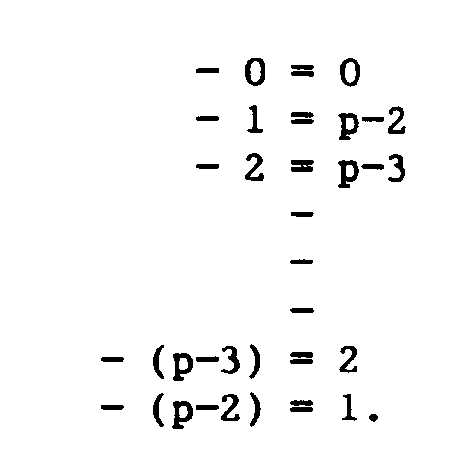
Thus, when specific values of (x-y) are converted to their negatives by means ofconverter circuit 15 of Figure 2, these negatives themselves directly map in turn to unique values which, for the most part, will be different to the specific values originally converted. Thus, with the apparatus of Figure 2, the Zech look-uptable circuit 2 need not contain entries corresponding to the said specific values of (x-y), provided that it does contain entries corresponding to the unique values to which the negatives of the said specific values directly map. In fact a reduction in size of the Zech look-uptable circuit 2 of approaching one half is made possible by the provision of thecircuits table circuit 2 quoted in the preamble) then theconverter circuit 15 may be arranged, for example, to produce the following relationship between the values of (x-y) represented at itsinput 24 and the resulting values of k represented at itsoutput 25.
(This is possible because -7=5 modulo 12, -8=4 modulo 12, etc.). Thedetector circuit 22 then has to be arranged to controlmultiplexer 18 to couple itsinput 16 to itsoutput 17 for values of (x-y) between 7 and 11, and to couple itsinput 19 to itsoutput 17 otherwise, thereby ensuring that the value i represented at theoutput 14 is correct is all cases. The result is that Zech look-uptable circuit 2 no longer needs to contain entries corresponding to values of (x-y) between 7 and 11. Of course, the choice of values of (x-y) between 7 and 11 for conversion to their negatives is merely one of several possibilities; any other set of values, or even just one or two values, may be chosen as desired, provided always that for each value v chosen, the value p-1-v (being the value to which its negative uniquely maps) is not also chosen. - If, for example,
subtractor 6 is arranged to generate each of the above-quoted values of (x-y) as a logic "1" on a respective one of thirteen output lines,converter 15 may be formed as a set of eight through-connections, those ranking third to seventh including respective OR-gates second inputs of which are fed from respective further input lines ranking thirteenth to ninth. In such acase detector circuit 22 may be formed by a six-input further OR-gate five respective inputs of which are fed from respective ones of the further input lines and the remaining input of which is fed from theinput 11 in such manner that a logic "1" is applied thereto when the input quantity y of the apparatus is "nil". Thus, for example, the said remaining input may be fed from the output of a further detector (not shown) for the presence of a representation of "nil" at theinput 11 or, if the value of the input quantity y is arranged to be represented by a logic "1" on a respective one of thirteen input lines constituting theinput 11, directly from the input line corresponding to "nil". The feeding of one input of the further OR-gate from theinput 11 in this way (indicated in Figure 2 by the dashed line 34) is provided because, when the value of the input quantity y of the apparatus of Figure 2 is "nil" (this itself being a power representation of Y=0) the resulting output fromadder 3 should be a quantity which is a power representation of X, i.e. x. Under these circumstances the output of subtractor 1 will be "nil" and that of look-up table 2 will be zero. Thus a representation of "nil" atinput 11 should be arranged to result in the controlling ofmultiplexer 18 to connect itsinput 16 to itsoutput 17, thereby ensuring that the input quantity x is transferred to theinput 12 ofadder 3 when y="nil". (As an alternative to arranging thatmultiplexer 18 responds to y="nil" in this way it is of course possible to provide a further multiplexer (not shown) having one signal input connected to input 10 and the other signal input connected tooutput 14, this multiplexer being controlled by the output signal of the said further detector or the line ofinput 11 corresponding to "nil", in such manner that it connects the one signal input to its output when y=nil and connects the other signal input to its output otherwise). Obviously, when (x-y) has a value such that its negative maps to the same value, e.g. 0 and 6 when p-1=12, it does not matter whichstate multiplexer 18 is controlled to adopt. - If desired the apparatus described with reference to Figure 2 may incorporate further features as described in the European publication EP-A- 4 025 533 of even date in order that the representations of i will be generated at the
output 14 of the apparatus in the form of n residue components modulo respective integers which are mutually prime and the product of which is equal to (p-1) and in order that the respresentations of x and y can be supplied to theinputs modulo 3 subtractor circuit operating in parallel on the corresponding residue components of the quantities x and y and theadder circuit 3 similarly being constituted by a modulo 4 adder circuit and amodulo 3 adder circuit operating in parallel on the corresponding residue components of the quantities j and m. If this is the case the output quantity (x-y) of subtractor subcircuit 1 will also be in the form of two residue components modulo 4 and 3 respectively, and if for example subtractor circuit 1 is constructed to generate representations of values from 0 to 3 of the first of these in the form of logic "1" onoutput lines output lines converter circuit 15 anddetector circuit 22 may be constructed, for example, as shown in Figure 3, i.e. by means of six NAND-gates 26-31, one OR-gate 32 and oneinverter 33 interconnected as shown. The output quantity for application to look-uptable circuit 2 is represented by a logic "1" on one of the outputs k0₃, k1₃ and k2₃ in combination with a logic "1" on one of the outputs k0₄, k1₄ and k2₄. A value of three for the modulo 4 input residue component, represented by logic "1" on input line 3₄, is converted to its negative by means of OR-gate 32 and appears as a logic "1" on output line k1₄. (-3 mod 4 = 1). Each time this occursNAND gates inverter 33, causing any logic "1" oninput line 1₃ orinput line 2₃ to be transferred to output line k1₃ or output line k2₃ respectively, are disabled. The result is that, instead, any logic "1" oninput line 1₃ is transferred to output line k2₃ and any logic "1" oninput line 2₃ is transferred to output line k1₃, i.e. any value of themodulo 3 input residue component represented by a logic "1" on one of the input lines 0₃, 1₃ and 2₃ is converted to its negative represented by a logic "1" on one of the output lines k0₃, k1₃ and k2₃. (-0mod 3 = 0, -1mod 3 = 2 and -2mod 3 = 1). It will be noted thatdetector 22 has in this simple example been replaced by a simple direct connection from input line 3₄ tooutput 21, the signal applied tooutput 22 also being used to control the conversion of themodulo 3 input residue component to its negative when required. Construction ofconverter circuit 15 as shown in Figure 3 makes it unnecessary for Zech look-up table 2 to contain entries corresponding to values of (x-y) of 3, 7 and 11. - The adder, subtractor and Zech look-up
table circuits - Further modifications to the embodiments described are possible. In particular different, and usually larger, values of p may be employed. For example, a value of 31 may be chosen for p, in which case subtractor circuit 1 and
adder circuit 3 may each be constituted by three parallel-operating subcircuits operating modulo 2, modulo 3 and modulo 5 respectively. - Although, as described, the same coding scheme is used for the quantities represented throughout the apparatus, it will be evident that this is not necessarily the case. For example, a one-out-of-N coding scheme may be used for the quantities x, y and i whereas the subtractor circuit 1, the look-up table 2 and the
converter circuit 15 may be constructed to produce their outputs in the form of a conventional compact binary code, the look-up table 2, thedetector circuit 22, and theadder circuit 3 being modified accordingly so as to respond in the desired manner to the compact binary codes used. - It will be evident that, because the processing takes place in the apparatus described in four distinct stages, i.e. subtraction, conversion/multiplexing, look-up and addition, so-called "pipelining" may readily be employed to optimise the processing throughput for a succession of input operands.
Claims (2)
- Apparatus for generating a representation modulo (p-1) of the power index i to which a generator g has to be raised to give the value (X + Y) in modulo p arithmetic in response to the application to said apparatus of representations modulo (p-1) of x, where gx=X, and y, where gy=Y, which apparatus has first and second inputs (10,11) for the representations of x and y respectively and an output (14) for the representation of i, said apparatus comprising
a subtractor circuit (1) having first and second inputs (4,5) coupled to said first and second inputs (10,11) respectively of the apparatus, for generating a representation modulo (p-1) of (x-y) at an output (6) thereof,
a look-up table circuit (2) having an input (7) coupled to the output (6) of the subtractor circuit (1), for generating at an output (8) thereof a representation modulo (p-1) of the power index j to which g has to be raised to give the value gk+1 in modulo p arithmetic in response to the application to said input (7) of a representation modulo (p-1) of any number of a set of values of k, and
an adder circuit (3) having first (12) and second (9) adder inputs to which are coupled the second input (11) of the apparatus and the output (8) of the look-up table circuit (2) respectively, for generating at an adder output (13) a representation modulo (p-1) of m+j in response to the application to its first and second adder inputs (9,12) of residue representations modulo (p-1) of m and j respectively, which adder output (13) constitutes the output (14) of the apparatus, characterised in that the apparatus further includes(a) a multiplexer circuit (18) having a first input (16), a second input (19), a control input (20) and an output (17), which multiplexer circuit (18) is controllable by the application of a control signal to said control input (20) to couple its first input (16) to its output (17) and its second input (19) to its output (17) as alternatives, said first input (16) being coupled to the first input (10) of the apparatus and the coupling from the second input (11) of the apparatus to the first adder input (12) being through said multiplexer circuit (18) from its second input (19) to its output (17),(b) a converter circuit (15) included in the coupling from the output (6) of the subtractor circuit (1) to the input of the look-up table circuit (2) for converting each representation of at least one specific value of (x-y) generated by the subtractor circuit (1) to a representation modulo (p-1) of (y-x), and(c) a coupling (22) from the output (6) of the subtractor circuit (1) to the control input (20) of the multiplexer circuit (18) for controlling the multiplexer circuit (18) to couple its first input (16) to its output (17) in response at least to the presence at the subtractor circuit output (6) of any representation of said at least one specific value of (x-y) which will be so converted by the converter circuit (15.) - Apparatus as claimed in Claim 1, including means for also controlling the multiplexer circuit (18) to couple its first input (16) to its output (17) in response to the presence at the second input of the apparatus of a representation of a specific value of y corresponding to Y=0.
Priority Applications (1)
| Application Number | Priority Date | Filing Date | Title |
|---|---|---|---|
| DE1989619077 DE68919077T2 (en) | 1989-06-12 | 1989-06-12 | Residual arithmetic device. |
Applications Claiming Priority (1)
| Application Number | Priority Date | Filing Date | Title |
|---|---|---|---|
| GB8810165A GB2217882B (en) | 1988-04-29 | 1988-04-29 | Arithmetic apparatus |
Publications (2)
| Publication Number | Publication Date |
|---|---|
| EP0402532A1 EP0402532A1 (en) | 1990-12-19 |
| EP0402532B1 true EP0402532B1 (en) | 1994-10-26 |
Family
ID=10636091
Family Applications (1)
| Application Number | Title | Priority Date | Filing Date |
|---|---|---|---|
| EP89201506A Expired - Lifetime EP0402532B1 (en) | 1988-04-29 | 1989-06-12 | Residue arithmetic apparatus |
Country Status (3)
| Country | Link |
|---|---|
| US (1) | US4994994A (en) |
| EP (1) | EP0402532B1 (en) |
| GB (1) | GB2217882B (en) |
Families Citing this family (8)
| Publication number | Priority date | Publication date | Assignee | Title |
|---|---|---|---|---|
| US5293607A (en) * | 1991-04-03 | 1994-03-08 | Hewlett-Packard Company | Flexible N-way memory interleaving |
| JPH0720778A (en) * | 1993-07-02 | 1995-01-24 | Fujitsu Ltd | Residue calculation device, table creation device and multiplication remainder calculation device |
| US5623423A (en) * | 1994-12-12 | 1997-04-22 | Univ. Of Texas | Apparatus and method for video decoding |
| DE10200133B4 (en) * | 2002-01-04 | 2005-12-22 | Infineon Technologies Ag | Method and device for calculating modulo operations |
| US7512230B2 (en) * | 2002-04-30 | 2009-03-31 | She Alfred C | Method and apparatus of fast modular reduction |
| JP4279626B2 (en) * | 2003-07-31 | 2009-06-17 | 株式会社アドバンテスト | Remainder calculation system, scaling calculator, scaling calculation method, program thereof and recording medium |
| US7849125B2 (en) | 2006-07-07 | 2010-12-07 | Via Telecom Co., Ltd | Efficient computation of the modulo operation based on divisor (2n-1) |
| JP4905161B2 (en) * | 2007-01-31 | 2012-03-28 | 富士通株式会社 | RAID device and data restoration device using Galois field |
Family Cites Families (1)
| Publication number | Priority date | Publication date | Assignee | Title |
|---|---|---|---|---|
| US4742479A (en) * | 1985-03-25 | 1988-05-03 | Motorola, Inc. | Modulo arithmetic unit having arbitrary offset and modulo values |
-
1988
- 1988-04-29 GB GB8810165A patent/GB2217882B/en not_active Expired - Lifetime
-
1989
- 1989-05-01 US US07/345,392 patent/US4994994A/en not_active Expired - Fee Related
- 1989-06-12 EP EP89201506A patent/EP0402532B1/en not_active Expired - Lifetime
Also Published As
| Publication number | Publication date |
|---|---|
| GB2217882B (en) | 1992-06-10 |
| GB2217882A (en) | 1989-11-01 |
| US4994994A (en) | 1991-02-19 |
| GB8810165D0 (en) | 1988-06-02 |
| EP0402532A1 (en) | 1990-12-19 |
Similar Documents
| Publication | Publication Date | Title |
|---|---|---|
| US5724276A (en) | Logic block structure optimized for sum generation | |
| US20050187997A1 (en) | Flexible accumulator in digital signal processing circuitry | |
| US4366549A (en) | Multiplier with index transforms modulo a prime or modulo a fermat prime and the fermat prime less one | |
| US4994994A (en) | Apparatus performing modulo p addition, where operands are expressed as powers of a generator, using a reduced size zech look-up table | |
| US4346451A (en) | Dual moduli exponent transform type high speed multiplication system | |
| US4706211A (en) | Digital multiplying circuit | |
| US4628472A (en) | Binary multiplier using ternary code | |
| EP0352029B1 (en) | Transformation of divisor and dividend in digital division | |
| Sasao | MACDAS: Multi-level AND-OR circuit synthesis using two-variable function generators | |
| JP2803601B2 (en) | Inversion circuit of finite field element | |
| US5530664A (en) | Method and apparatus for automatically designing logic circuit, and multiplier | |
| US5008849A (en) | Apparatus adding values represented as residues in modulo arithmetic | |
| US6898613B1 (en) | Arithmetic circuits for use with the residue number system | |
| US5050120A (en) | Residue addition overflow detection processor | |
| US5249144A (en) | Programmable optical arithmetic/logic unit | |
| Tanaka et al. | Novel binary signed-digit addition algorithm for FPGA implementation | |
| Lindström et al. | Arithmetic circuits combining residue and signed-digit representations | |
| KR100480997B1 (en) | APPARATUS OF FIELD MULTIPLICATION OVER GF(p) AND GF(2^m) | |
| Wei et al. | Residue arithmetic circuits based on the signed-digit multiple-valued arithmetic circuits | |
| Radhakrishnan et al. | A fast RNS Galois field multiplier | |
| Sahu et al. | Improved redundant binary adder realization in FPGA | |
| US5084835A (en) | Method and apparatus for absolute value summation and subtraction | |
| US3798434A (en) | Electronic device for quintupling a binary-coded decimal number | |
| US5954791A (en) | Multipliers with a shorter run time | |
| Wei et al. | Compact residue arithmetic multiplier based on the radix-4 signed-digit multiple-valued arithmetic circuits |
Legal Events
| Date | Code | Title | Description |
|---|---|---|---|
| PUAI | Public reference made under article 153(3) epc to a published international application that has entered the european phase |
Free format text: ORIGINAL CODE: 0009012 |
|
| AK | Designated contracting states |
Kind code of ref document: A1 Designated state(s): DE FR GB |
|
| 17P | Request for examination filed |
Effective date: 19910613 |
|
| RAP3 | Party data changed (applicant data changed or rights of an application transferred) |
Owner name: N.V. PHILIPS' GLOEILAMPENFABRIEKEN Owner name: PHILIPS ELECTRONICS UK LIMITED |
|
| 17Q | First examination report despatched |
Effective date: 19931220 |
|
| GRAA | (expected) grant |
Free format text: ORIGINAL CODE: 0009210 |
|
| AK | Designated contracting states |
Kind code of ref document: B1 Designated state(s): DE FR GB |
|
| REF | Corresponds to: |
Ref document number: 68919077 Country of ref document: DE Date of ref document: 19941201 |
|
| ET | Fr: translation filed | ||
| REG | Reference to a national code |
Ref country code: FR Ref legal event code: CD |
|
| PLBE | No opposition filed within time limit |
Free format text: ORIGINAL CODE: 0009261 |
|
| STAA | Information on the status of an ep patent application or granted ep patent |
Free format text: STATUS: NO OPPOSITION FILED WITHIN TIME LIMIT |
|
| 26N | No opposition filed | ||
| PGFP | Annual fee paid to national office [announced via postgrant information from national office to epo] |
Ref country code: GB Payment date: 19960603 Year of fee payment: 8 |
|
| PG25 | Lapsed in a contracting state [announced via postgrant information from national office to epo] |
Ref country code: GB Free format text: LAPSE BECAUSE OF NON-PAYMENT OF DUE FEES Effective date: 19970612 |
|
| PGFP | Annual fee paid to national office [announced via postgrant information from national office to epo] |
Ref country code: FR Payment date: 19970624 Year of fee payment: 9 |
|
| PGFP | Annual fee paid to national office [announced via postgrant information from national office to epo] |
Ref country code: DE Payment date: 19970822 Year of fee payment: 9 |
|
| GBPC | Gb: european patent ceased through non-payment of renewal fee |
Effective date: 19970612 |
|
| PG25 | Lapsed in a contracting state [announced via postgrant information from national office to epo] |
Ref country code: FR Free format text: LAPSE BECAUSE OF NON-PAYMENT OF DUE FEES Effective date: 19990226 |
|
| PG25 | Lapsed in a contracting state [announced via postgrant information from national office to epo] |
Ref country code: DE Free format text: LAPSE BECAUSE OF NON-PAYMENT OF DUE FEES Effective date: 19990401 |
|
| REG | Reference to a national code |
Ref country code: FR Ref legal event code: ST |