EP0400877A2 - Contact metallization of semiconductor integrated circuit devices - Google Patents
Contact metallization of semiconductor integrated circuit devices Download PDFInfo
- Publication number
- EP0400877A2 EP0400877A2 EP90305583A EP90305583A EP0400877A2 EP 0400877 A2 EP0400877 A2 EP 0400877A2 EP 90305583 A EP90305583 A EP 90305583A EP 90305583 A EP90305583 A EP 90305583A EP 0400877 A2 EP0400877 A2 EP 0400877A2
- Authority
- EP
- European Patent Office
- Prior art keywords
- silicide
- forming material
- contact
- region
- titanium
- Prior art date
- Legal status (The legal status is an assumption and is not a legal conclusion. Google has not performed a legal analysis and makes no representation as to the accuracy of the status listed.)
- Ceased
Links
Images

Classifications
-
- H10D64/0112—
-
- H10W20/031—
-
- H10W20/425—
Definitions
- the invention is concerned with semiconductor integrated-circuit devices including a metallization.
- Making electrical contact to semiconductor regions such as, e.g., source, drain, and gate regions of a field-effect transistor typically involves the deposition of a metallization over a dielectric which has been patterned to produce openings (windows, holes, vias) to the underlying semiconductor structure.
- a metallization over a dielectric which has been patterned to produce openings (windows, holes, vias) to the underlying semiconductor structure.
- aluminum is the material most widely used for semiconductor device metallization
- other materials such as, e.g., tungsten and cobalt are also receiving attention.
- contact structures have been proposed including one or more additional layers intermediate to metallization and semiconductor materials: for example, in the case of source and drain regions in silicon devices, a layer of titanium silicide is advantageously included between the silicon semiconductor and aluminum metallization materials.
- U.S. patent 4,361,599, issued November 30, 1982 to R. L. Wourms discloses a plasma-etching process for making contact openings in a dielectric material, underlying silicide regions serving to inhibit over-etching;
- contact structures in semiconductor integrated-circuit devices have low contact resistance, good step coverage, and protection against interdiffusion and electromigration.
- a contact structure comprising a silicide layer and a metallization layer, and especially to the interface between such layers.
- electrical contacts preferably are made by a method which includes, after window etching, steps of depositing silicide-forming material and annealing in a non-oxidizing atmosphere; preferably, such atmosphere promotes the formation of a conductive compound with the silicide-forming material. After annealing, contact metal is deposited. Processing in accordance with the invention is of particular interest as applied to devices in which window size is less than or equal to 1 micrometer.
- Preferred metallizations comprise aluminum, and titanium is preferred as a silicide-forming material.
- the non-oxidizing atmosphere comprises nitrogen.
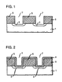
- FIG. 1 shows substrate 1, contact regions 3, and dielectric layer 5, with openings 7 exposing portions of regions 3; such openings typically are made by photolithographic processing involving etching in the presence of a patterned mask layer.
- Contact openings may be, e.g., to source or drain regions of field-effect transistors, or to contact regions intended for device interconnection. Typically, in the latter case, contact is made to silicon in polycrystalline form. Contact regions typically comprise heavily doped silicon, and they may further comprise a surface region of a silicide such as, e.g., titanium silicide which was formed prior to deposition of dielectric layer 5.
- the dielectric may consist essentially of an oxide.
- FIG. 2 shows the device of FIG. 1 after further processing involving the deposition of silicide-forming layer 9, exemplary device features 1, 3, 5, and 7 here and throughout being the same as in FIG. 1.
- Layer 9 may consist essentially of titanium, and deposition may be sputtering; the choice of material and of the deposition method is influenced by considerations of adhesion and step coverage. In the case of titanium, preferred thickness of layer 9 is in a range from 10 to 100 nanometers, 60 nanometers being typical.
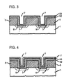
- preferred processing calls for (rapid) thermal annealing in a non-oxidizing atmosphere such as, e.g., a nitrogen atmosphere; such annealing involves (short-term) heating at an elevated temperature, e.g., by exposure to infrared radiation.
- a non-oxidizing atmosphere such as, e.g., a nitrogen atmosphere
- preferred annealing is at a temperature in the range from 750 to 950 degrees C for a duration in the range from 10 seconds to 1 minute, lower temperatures corresponding to longer times and conversely.
- An exemplary temperature is approximately 800 degrees C, with a corresponding time of approximately 20 seconds.
- time and temperature may be chosen to effect substantial conversion of the material of layer 9 into (i) silicide adjacent to the substrate, and (ii) a conductive surface compound with an atmospheric constituent such as, e.g., nitrogen.
- a conductive surface compound with an atmospheric constituent such as, e.g., nitrogen.
- annealing fosters replenishment of silicide lost in the course of window etching.
- annealing may result in the removal of surface oxides and contaminants.
- FIG. 3 shows the device of FIG. 2 after annealing, layer 9 now comprising sublayers 91, 92, and 93.
- Layer 91 consists essentially of silicide as formed due to reaction of deposited silicide-forming material with silicon
- layer 92 consists essentially of unreacted silicide-forming material
- layer 93 consists essentially of a nitride of the silicide-forming material, as illustrative of the case in which the annealing atmosphere comprises nitrogen.
- FIG. 4 shows the device of FIG. 3 after further deposition of a metallization layer 11, typically consisting essentially of aluminum comprising a small amount of silicon or copper, and having a thickness which is in a typical range from 400 nanometers to 1.2 micrometers. At this point, the device is ready for further processing as is well-understood in the art.
- a metallization layer 11 typically consisting essentially of aluminum comprising a small amount of silicon or copper, and having a thickness which is in a typical range from 400 nanometers to 1.2 micrometers.
- CMOS complementary metal-oxide semiconductor
- CMOS complementary metal-oxide semiconductor
- a conductive compound can further serve as a built-in safeguard and electrical path in case of interruption of the metallization due to electromigration.
- Processing of the invention may also involve metallization metals other than aluminum, tungsten being considered a particularly suitable alternative.
- a deposited silicide-forming material may be alloyed not only with the underlying silicon, but also with the metallization, and this will apply especially in the case of a tungsten metallization.
- materials other than titanium suitable as a silicide-forming material, are cobalt, platinum, and alloys of titanium, cobalt, and platinum.
- nitrogen suitable as an inert atmospheric constituent during annealing, argon or helium may be used, as well as mixtures of such gases.
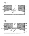
- FIG. 5-8 show field oxide 51 and doped region 52.
- substrate 1 is p-doped
- region 52 is doped n+, e.g., with arsenic and/or phosphorus.
- the substrate is n-doped
- region 52 is doped p+, e.g., with boron.
- window 7 is shown etched such that not only a portion of silicide region 3 is uncovered but, due to (unintended) misalignment, also a portion of substrate 1.
- window 7 is shown etched such that not only a portion of silicide region 3 is uncovered but, due to (unintended) misalignment, also a portion of substrate 1.
- such latter portion would be ineffective as part of the intended contact, and its presence would lead to shorting between a doped tub in the substrate and a source or drain contact.
- Such inefficacy and shorting are prevented by preferred processing in accordance with the invention in that the junction is extended essentially coextensive with the window as etched.
- silicide-forming layer 9 (FIG. 6), and as a result of annealing (FIG. 7), impurities have diffused laterally, resulting in extension of doped region 52.
- arsenic is preferred as n-type dopant on account of its high diffusivity in silicide.
- silicide 91 extends over the newly doped region, thereby resulting in the formation of an efficacious contact in spite of misalignment of the window.
- the final structure including metallization layer 11 is shown in FIG. 8.
- CMOS complementary metal-oxide semiconductor
- NMOS-dominated devices such as, e.g., dynamic random-access memory (DRAM) arrays.
- DRAM dynamic random-access memory
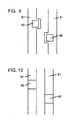
- preferred processing may permit the use of so-called headless contacts to active areas whose width is the same as the window width -- thus permitting the use of more narrow active areas, and closer spacing of active areas on a chip. This is illustrated by FIG. 9 and 10 which show two adjacent active areas 81, and windows 82.
- windows 82 are etched at widened portions of the active area 81 as is typical in prior-art practice. Widened areas are included to provide a margin of window misalignment relative to the active area, as well as a margin of window oversize as may occur during window patterning.
- FIG. 10 illustrates the use of an active area 81 which nominally has the same width as windows 82, as made practicable due to processing in accordance with the invention, potential window misalignment or oversize being compensated for by extension of the junction as described above. It is readily apparent upon inspection of FIG. 9 and 10 that, given a specified window size and a specified minimum distance between adjacent active areas, less space is occupied by the active areas in FIG. 10 as compared with FIG. 9.
Landscapes
- Electrodes Of Semiconductors (AREA)
- Internal Circuitry In Semiconductor Integrated Circuit Devices (AREA)
- Insulated Gate Type Field-Effect Transistor (AREA)
Abstract
Description
- The invention is concerned with semiconductor integrated-circuit devices including a metallization.
- Making electrical contact to semiconductor regions such as, e.g., source, drain, and gate regions of a field-effect transistor typically involves the deposition of a metallization over a dielectric which has been patterned to produce openings (windows, holes, vias) to the underlying semiconductor structure. While, currently, aluminum is the material most widely used for semiconductor device metallization, other materials such as, e.g., tungsten and cobalt are also receiving attention. And, primarily in the interest of reduced contact resistance, contact structures have been proposed including one or more additional layers intermediate to metallization and semiconductor materials: for example, in the case of source and drain regions in silicon devices, a layer of titanium silicide is advantageously included between the silicon semiconductor and aluminum metallization materials.
- Contact structures and methods for their fabrication have evolved as motivated by a variety of concerns relating not only to contact resistance, but also to step coverage, to electromigration, and to interdiffusion. The following background art is considered as representative in addressing such concerns:
- U.S. patent 4,107,726, issued August 15, 1978 to H. Schilling, discloses metallizations in which aluminum overlies a thin layer of titanium which, in turn, overlies a layer of platinum silicide in contact windows;
- U.S. patent 4,361,599, issued November 30, 1982 to R. L. Wourms discloses a plasma-etching process for making contact openings in a dielectric material, underlying silicide regions serving to inhibit over-etching;
- U.S. patent 4,398,335, issued August 16, 1983 to W. I. Lehrer discloses a silicide metallization which is made by depositing silicon on a dielectric, followed by depositing of a silicide-forming material;
- U.S. patent 4,502,209, issued March 5, 1985 to M. E. Eizenberg et al. discloses exemplary contact structures comprising layers of aluminum, titanium carbide, and titanium silicide on silicon, as well as other, similar multi-layer metallization structures.
- Quite generally, desirable contact structures in semiconductor integrated-circuit devices have low contact resistance, good step coverage, and protection against interdiffusion and electromigration. In the following, with such desiderata in mind, attention is directed to a contact structure comprising a silicide layer and a metallization layer, and especially to the interface between such layers.
- In the manufacture of semiconductor integrated-circuit devices, electrical contacts preferably are made by a method which includes, after window etching, steps of depositing silicide-forming material and annealing in a non-oxidizing atmosphere; preferably, such atmosphere promotes the formation of a conductive compound with the silicide-forming material. After annealing, contact metal is deposited. Processing in accordance with the invention is of particular interest as applied to devices in which window size is less than or equal to 1 micrometer. Preferred metallizations comprise aluminum, and titanium is preferred as a silicide-forming material. Preferably, in the latter case, the non-oxidizing atmosphere comprises nitrogen.
-
- FIG. 1-4 are enlarged side views of a first exemplary device at different stages of preferred metallization processing of the invention;
- FIG. 5-8 are enlarged side views of a second exemplary device at different stages of preferred metallization processing of the invention; and
- FIG. 9 and 10 are enlarged top views of windows etched into a dielectric as placed relative to underlying semiconductor active areas.
- For the sake of clarity, the elements of the devices depicted in the Figures are not drawn to scale.
- FIG. 1 shows
substrate 1,contact regions 3, anddielectric layer 5, withopenings 7 exposing portions ofregions 3; such openings typically are made by photolithographic processing involving etching in the presence of a patterned mask layer. - Contact openings may be, e.g., to source or drain regions of field-effect transistors, or to contact regions intended for device interconnection. Typically, in the latter case, contact is made to silicon in polycrystalline form. Contact regions typically comprise heavily doped silicon, and they may further comprise a surface region of a silicide such as, e.g., titanium silicide which was formed prior to deposition of
dielectric layer 5. The dielectric may consist essentially of an oxide. - FIG. 2 shows the device of FIG. 1 after further processing involving the deposition of silicide-forming
layer 9, exemplary device features 1, 3, 5, and 7 here and throughout being the same as in FIG. 1.Layer 9 may consist essentially of titanium, and deposition may be sputtering; the choice of material and of the deposition method is influenced by considerations of adhesion and step coverage. In the case of titanium, preferred thickness oflayer 9 is in a range from 10 to 100 nanometers, 60 nanometers being typical. - At this point, preferred processing calls for (rapid) thermal annealing in a non-oxidizing atmosphere such as, e.g., a nitrogen atmosphere; such annealing involves (short-term) heating at an elevated temperature, e.g., by exposure to infrared radiation. For a 60-nanometer layer of titanium, preferred annealing is at a temperature in the range from 750 to 950 degrees C for a duration in the range from 10 seconds to 1 minute, lower temperatures corresponding to longer times and conversely. An exemplary temperature is approximately 800 degrees C, with a corresponding time of approximately 20 seconds. More generally, time and temperature may be chosen to effect substantial conversion of the material of
layer 9 into (i) silicide adjacent to the substrate, and (ii) a conductive surface compound with an atmospheric constituent such as, e.g., nitrogen. In the case of windows to formerly silicided regions, annealing fosters replenishment of silicide lost in the course of window etching. Also, annealing may result in the removal of surface oxides and contaminants. - FIG. 3 shows the device of FIG. 2 after annealing,
layer 9 now comprisingsublayers Layer 91 consists essentially of silicide as formed due to reaction of deposited silicide-forming material with silicon,layer 92 consists essentially of unreacted silicide-forming material, andlayer 93 consists essentially of a nitride of the silicide-forming material, as illustrative of the case in which the annealing atmosphere comprises nitrogen. - FIG. 4 shows the device of FIG. 3 after further deposition of a
metallization layer 11, typically consisting essentially of aluminum comprising a small amount of silicon or copper, and having a thickness which is in a typical range from 400 nanometers to 1.2 micrometers. At this point, the device is ready for further processing as is well-understood in the art. - Preferred processing in accordance with the invention may be used, e.g., in the manufacture of complementary metal-oxide semiconductor (CMOS) devices, including n-channel and p-channel field-effect transistors on a common substrate. Such processing yields metallizations with good step coverage and, when a preferred conductive compound is formed between the silicide and the metallization, with protection against interdiffusion or "spiking". A conductive compound can further serve as a built-in safeguard and electrical path in case of interruption of the metallization due to electromigration.
- Processing of the invention may also involve metallization metals other than aluminum, tungsten being considered a particularly suitable alternative. Also, a deposited silicide-forming material may be alloyed not only with the underlying silicon, but also with the metallization, and this will apply especially in the case of a tungsten metallization. Among materials other than titanium, suitable as a silicide-forming material, are cobalt, platinum, and alloys of titanium, cobalt, and platinum. Other than nitrogen, suitable as an inert atmospheric constituent during annealing, argon or helium may be used, as well as mixtures of such gases.
- A further benefit of preferred processing in accordance with the invention relates to tolerance with respect to misalignment of etched windows relative to the semiconductor structure. This aspect of the invention is illustrated by FIG. 5-8 which, in addition to features described above in connection with FIG. 1-4,
show field oxide 51 and dopedregion 52. In the case of an n-channel device,substrate 1 is p-doped, andregion 52 is doped n⁺, e.g., with arsenic and/or phosphorus. In the case of a p-channel device, the substrate is n-doped, andregion 52 is doped p⁺, e.g., with boron. - In FIG. 5,
window 7 is shown etched such that not only a portion ofsilicide region 3 is uncovered but, due to (unintended) misalignment, also a portion ofsubstrate 1. In accordance with prior-art deposition of a metallization, such latter portion would be ineffective as part of the intended contact, and its presence would lead to shorting between a doped tub in the substrate and a source or drain contact. Such inefficacy and shorting are prevented by preferred processing in accordance with the invention in that the junction is extended essentially coextensive with the window as etched. - More specifically, after deposition of silicide-forming layer 9 (FIG. 6), and as a result of annealing (FIG. 7), impurities have diffused laterally, resulting in extension of
doped region 52. (In this respect, arsenic is preferred as n-type dopant on account of its high diffusivity in silicide.) Also, additionally formedsilicide 91 extends over the newly doped region, thereby resulting in the formation of an efficacious contact in spite of misalignment of the window. The final structure includingmetallization layer 11 is shown in FIG. 8. - Further to processing as described above, in the interest of supplying additional n-type dopant to formerly undoped window regions, it may be desirable to include a step of phosphorus implantation prior to deposition of silicide-forming material. In this respect, in the case of CMOS processing, a dose not exceeding approximately 10¹⁴/cm² may be chosen so as to avoid excessive counterdoping of exposed contact areas of p-channel devices. Higher doses may be preferred in the case of n-channel metal-oxide semiconductor (NMOS) device processing.
- Tolerance to misalignment is particularly beneficial in the manufacture of NMOS-dominated devices such as, e.g., dynamic random-access memory (DRAM) arrays. In such and similar devices, preferred processing may permit the use of so-called headless contacts to active areas whose width is the same as the window width -- thus permitting the use of more narrow active areas, and closer spacing of active areas on a chip. This is illustrated by FIG. 9 and 10 which show two adjacent
active areas 81, andwindows 82. - In FIG. 9,
windows 82 are etched at widened portions of theactive area 81 as is typical in prior-art practice. Widened areas are included to provide a margin of window misalignment relative to the active area, as well as a margin of window oversize as may occur during window patterning. - FIG. 10, by contrast, illustrates the use of an
active area 81 which nominally has the same width aswindows 82, as made practicable due to processing in accordance with the invention, potential window misalignment or oversize being compensated for by extension of the junction as described above. It is readily apparent upon inspection of FIG. 9 and 10 that, given a specified window size and a specified minimum distance between adjacent active areas, less space is occupied by the active areas in FIG. 10 as compared with FIG. 9.
Claims (16)
depositing a dielectric layer on said body,
etching an opening to said region into said dielectric layer,
depositing silicide-forming material,
heating in a non-oxidizing atmosphere, and
depositing a metal layer.
a first region comprising a silicide of a first material,
a second region comprising a conductive compound of said first material with a second material, and
a metal.
Applications Claiming Priority (2)
| Application Number | Priority Date | Filing Date | Title |
|---|---|---|---|
| US35945089A | 1989-05-31 | 1989-05-31 | |
| US359450 | 1989-05-31 |
Publications (2)
| Publication Number | Publication Date |
|---|---|
| EP0400877A2 true EP0400877A2 (en) | 1990-12-05 |
| EP0400877A3 EP0400877A3 (en) | 1991-10-23 |
Family
ID=23413839
Family Applications (1)
| Application Number | Title | Priority Date | Filing Date |
|---|---|---|---|
| EP19900305583 Ceased EP0400877A3 (en) | 1989-05-31 | 1990-05-23 | Contact metallization of semiconductor integrated circuit devices |
Country Status (2)
| Country | Link |
|---|---|
| EP (1) | EP0400877A3 (en) |
| JP (1) | JPH0329321A (en) |
Cited By (3)
| Publication number | Priority date | Publication date | Assignee | Title |
|---|---|---|---|---|
| EP0607820A3 (en) * | 1993-01-08 | 1994-12-28 | Nippon Electric Co | Method for manufacturing a semiconductor device comprising a layer of metallic silicide on a diffused region. |
| EP0851493A1 (en) * | 1996-12-27 | 1998-07-01 | STMicroelectronics S.r.l. | Contact structure and corresponding manufacturing method for EPROM or flash EPROM semiconductor electronic devices |
| WO2001004947A1 (en) * | 1999-07-12 | 2001-01-18 | Advanced Micro Devices, Inc. | Method of compensating for material loss in a metal silicide layer in contacts of integrated circuit devices |
Families Citing this family (3)
| Publication number | Priority date | Publication date | Assignee | Title |
|---|---|---|---|---|
| KR940006689B1 (en) * | 1991-10-21 | 1994-07-25 | 삼성전자 주식회사 | Method of forming contact window of semiconductor device |
| JPH0837164A (en) * | 1994-07-21 | 1996-02-06 | Nec Corp | Method for manufacturing semiconductor device |
| KR100357186B1 (en) * | 2000-11-02 | 2002-10-19 | 주식회사 하이닉스반도체 | method for forming contact of semiconductor device |
Family Cites Families (1)
| Publication number | Priority date | Publication date | Assignee | Title |
|---|---|---|---|---|
| JPS61206243A (en) * | 1985-03-08 | 1986-09-12 | Mitsubishi Electric Corp | Semiconductor device using high melting-point metal electrode and wiring film |
-
1990
- 1990-05-23 EP EP19900305583 patent/EP0400877A3/en not_active Ceased
- 1990-05-30 JP JP2138657A patent/JPH0329321A/en active Pending
Cited By (5)
| Publication number | Priority date | Publication date | Assignee | Title |
|---|---|---|---|---|
| EP0607820A3 (en) * | 1993-01-08 | 1994-12-28 | Nippon Electric Co | Method for manufacturing a semiconductor device comprising a layer of metallic silicide on a diffused region. |
| EP0851493A1 (en) * | 1996-12-27 | 1998-07-01 | STMicroelectronics S.r.l. | Contact structure and corresponding manufacturing method for EPROM or flash EPROM semiconductor electronic devices |
| US6124169A (en) * | 1996-12-27 | 2000-09-26 | Stmicroelectronics, S.R.L. | Contact structure and associated process for production of semiconductor electronic devices and in particular nonvolatile EPROM and flash EPROM memories |
| WO2001004947A1 (en) * | 1999-07-12 | 2001-01-18 | Advanced Micro Devices, Inc. | Method of compensating for material loss in a metal silicide layer in contacts of integrated circuit devices |
| US6271122B1 (en) | 1999-07-12 | 2001-08-07 | Advanced Micro Devices, Inc. | Method of compensating for material loss in a metal silicone layer in contacts of integrated circuit devices |
Also Published As
| Publication number | Publication date |
|---|---|
| JPH0329321A (en) | 1991-02-07 |
| EP0400877A3 (en) | 1991-10-23 |
Similar Documents
| Publication | Publication Date | Title |
|---|---|---|
| US5102827A (en) | Contact metallization of semiconductor integrated-circuit devices | |
| US4333099A (en) | Use of silicide to bridge unwanted polycrystalline silicon P-N junction | |
| US4648175A (en) | Use of selectively deposited tungsten for contact formation and shunting metallization | |
| US3906540A (en) | Metal-silicide Schottky diode employing an aluminum connector | |
| CA1207469A (en) | Method of producing mos transistors | |
| JP2569327B2 (en) | Contact structures for silicon-based semiconductor devices | |
| JP3066041B2 (en) | Method of forming an integrated circuit including a highly resistive amorphous silicon resistor | |
| US5340751A (en) | Method of manufacturing a BiMOS device | |
| US5457062A (en) | Method for forming gigaohm load for BiCMOS process | |
| JPS61501358A (en) | Improved integrated circuit structure with intermediate metal silicide layer and method of fabrication thereof | |
| JP3626773B2 (en) | Conductive layer of semiconductor device, MOSFET, and manufacturing method thereof | |
| US5091322A (en) | Semiconductor device and method of manufacturing the same | |
| US4729969A (en) | Method for forming silicide electrode in semiconductor device | |
| US6495460B1 (en) | Dual layer silicide formation using a titanium barrier to reduce surface roughness at silicide/junction interface | |
| JPS592186B2 (en) | Complementary MOS device | |
| JPH0837164A (en) | Method for manufacturing semiconductor device | |
| EP0400877A2 (en) | Contact metallization of semiconductor integrated circuit devices | |
| JP3093620B2 (en) | Method for manufacturing semiconductor device | |
| US4476157A (en) | Method for manufacturing schottky barrier diode | |
| US5521416A (en) | Semiconductor device having gate electrode and impurity diffusion layer different in conductivity type and method of manufacturing the same | |
| KR100289372B1 (en) | A method of forming polycide | |
| KR0151038B1 (en) | Polyside contact of semiconductor device and forming method thereof | |
| JP3253438B2 (en) | Semiconductor device | |
| US20020068444A1 (en) | Dual layer silicide formation using an aluminum barrier to reduce surface roughness at silicide/junction interface | |
| JP3292154B2 (en) | Method for manufacturing semiconductor device |
Legal Events
| Date | Code | Title | Description |
|---|---|---|---|
| PUAI | Public reference made under article 153(3) epc to a published international application that has entered the european phase |
Free format text: ORIGINAL CODE: 0009012 |
|
| AK | Designated contracting states |
Kind code of ref document: A2 Designated state(s): DE ES FR GB IT NL |
|
| PUAL | Search report despatched |
Free format text: ORIGINAL CODE: 0009013 |
|
| AK | Designated contracting states |
Kind code of ref document: A3 Designated state(s): DE ES FR GB IT NL |
|
| 17P | Request for examination filed |
Effective date: 19920415 |
|
| RAP3 | Party data changed (applicant data changed or rights of an application transferred) |
Owner name: AT&T CORP. |
|
| 17Q | First examination report despatched |
Effective date: 19940614 |
|
| STAA | Information on the status of an ep patent application or granted ep patent |
Free format text: STATUS: THE APPLICATION HAS BEEN REFUSED |
|
| 18R | Application refused |
Effective date: 19950403 |