EP0392831A2 - Power transistor drive circuit with improved short circuit protection - Google Patents
Power transistor drive circuit with improved short circuit protection Download PDFInfo
- Publication number
- EP0392831A2 EP0392831A2 EP90303925A EP90303925A EP0392831A2 EP 0392831 A2 EP0392831 A2 EP 0392831A2 EP 90303925 A EP90303925 A EP 90303925A EP 90303925 A EP90303925 A EP 90303925A EP 0392831 A2 EP0392831 A2 EP 0392831A2
- Authority
- EP
- European Patent Office
- Prior art keywords
- voltage
- transistor
- emitter
- collector
- pair
- Prior art date
- Legal status (The legal status is an assumption and is not a legal conclusion. Google has not performed a legal analysis and makes no representation as to the accuracy of the status listed.)
- Withdrawn
Links
- 230000005611 electricity Effects 0.000 claims description 7
- 230000000295 complement effect Effects 0.000 claims description 5
- 230000008878 coupling Effects 0.000 claims description 5
- 238000010168 coupling process Methods 0.000 claims description 5
- 238000005859 coupling reaction Methods 0.000 claims description 5
- 230000007423 decrease Effects 0.000 description 4
- 239000004065 semiconductor Substances 0.000 description 3
- 230000002411 adverse Effects 0.000 description 2
- 230000000694 effects Effects 0.000 description 2
- 229920006395 saturated elastomer Polymers 0.000 description 2
- 238000010586 diagram Methods 0.000 description 1
- 238000000034 method Methods 0.000 description 1
- 230000004083 survival effect Effects 0.000 description 1
Images
Classifications
-
- H—ELECTRICITY
- H03—ELECTRONIC CIRCUITRY
- H03K—PULSE TECHNIQUE
- H03K17/00—Electronic switching or gating, i.e. not by contact-making and –breaking
- H03K17/08—Modifications for protecting switching circuit against overcurrent or overvoltage
- H03K17/082—Modifications for protecting switching circuit against overcurrent or overvoltage by feedback from the output to the control circuit
- H03K17/0828—Modifications for protecting switching circuit against overcurrent or overvoltage by feedback from the output to the control circuit in composite switches
Definitions
- the present invention relates to circuits for driving power transistors which control the application of electricity to a load; and more particularly to such circuits which provide some degree of protection against the adverse effects of a short circuit in the load coupled to the transistor.
- IGBT insulated gate bipolar transistors
- a desirable feature of this type of power semiconductor device is the capability of surviving short circuit load conditions by self-limiting the fault current rather than relying solely upon conventional protection techniques.
- This self-limiting capability is a function of the conductivity of the IGBT and the magnitude of the drive voltage applied to its gate electrode. Higher gate voltages permit a greater fault current to flow through the transistor; thereby increasing the stress on the device and likelihood that it will fail under a short circuit condition before a current sensor can act to turn off the transistor's gate drive. It is therefore advantageous from the aspect of short circuit survival to limit the conductivity of the transistor, but this has the adverse effect of raising the on-state voltage drop across the IGBT. A higher voltage drop results in a larger power loss in the device and more power dissipation. When the IGBT is switching several hundred amperes, a difference of a few volts across the device amounts to a significant power dissipation.
- the present circuit drives the gate of a IGBT power semiconductor in a manner which utilizes the short circuit protection capabilities of the device under fault conditions, while reducing the power loss in the device under normal operating load conditions.
- the circuit detects when the IGBT is in a state of saturation, e.g. by sensing the voltage across the collector and emitter of the transistor.
- the gate of the IGBT is driven at a first voltage level when the IGBT is in a saturated state (voltage across the collector and emitter is below a predetermined threshold).
- the gate electrode is driven at a second voltage level.
- the second voltage level reduces the conductivity of the transistor from the conductivity level when the gate is driven at the first voltage level.
- the transistor can tolerate the short circuit current for a longer period of time thereby enabling conventional protection circuits to operate before the transistor fails.
- the drive circuit increases the conductivity of the IGBT thereby reducing the voltage drop and power loss.
- circuit of the invention acts to fully turn on the power transistor under normal load conditions, but to reduce the conductivity of the transistor when a short circuit condition exists.
- a load 10 is coupled to a source of electrical power, such as a first battery 12, by an insulated gate bipolar transistor (IGBT) 13 and a conventional short circuit current sensor 11.
- the emitter of the IGBT 13 is connected to the negative terminal of the first battery 12 and the IGBT's collector is connected to the load 10 at a node 38.
- the IGBT 13 is turned on, the current from the first battery 12 flows through the load 10.
- the current sensor 11 reacts by applying a low logic level signal onto line 15. Otherwise, a high logic level signal is applied to line 15 by the current sensor 11.
- the IGBT 13 enables a relatively low voltage control signal, on the order of ten to twenty volts, to control the application of a relatively high voltage and current to the load, for example, 100 amperes at 550 volts.
- the load 10 is controlled by an input signal at terminal 14 which is coupled to one input of an AND gate 16.
- the other input of the AND gate is connected to line 15 from the current sensor 11.
- the gate 16 allows a digital logic level signal from an external control circuit to activate the IGBT 13. Specifically, under normal conditions, a high level voltage at terminal 14 turns on the application of electricity to the load, whereas a low level voltage applied to the terminal turns off that electricity.
- the output of the AND gate 16 is coupled by a current limiting resistor 18 to the base of an NPN transistor Q1.
- the emitter of transistor Q1 is directly coupled to circuit ground 20, which is connected to the negative terminal of a second battery 22.
- the second battery 22 supplies a low voltage (e.g. 15 volts) to the IGBT control circuit.
- the positive terminal of the second battery 22 is connected to a positive voltage bus 24.
- the collector of transistor Q1 is coupled by a pair of series connected resistors 26 and 28 to the positive voltage bus 24.
- transistor Q1 When the output of the AND gate 16 is high, transistor Q1 turns on reducing the voltage potential at the intermediate node 27 between resistors 26 and 28. This lower voltage, which is applied to the base of transistor Q2, turns on transistor Q2 thereby coupling one end of a voltage divider, consisting of resistors 30 and 32, to the positive voltage bus 24. In this state, approximately 15 volts is applied across this voltage divider to produce an intermediate voltage of approximately +10 volts at a second node 34 between resistors 30 and 32.
- the second node 34 is coupled to the bases of a pair of complementary conductivity type transistors Q4 and Q5 connected as an emitter follower between circuit ground 20 and the positive voltage bus 24. Specifically, the emitters of the complementary transistors Q4 and Q5 are connected together and their collectors are connected to the positive voltage bus 24 and circuit ground 20, respectively. The magnitude of the voltage appearing at the emitters of transistors Q4 and Q5 corresponds to the magnitude of the voltage applied to their base electrodes which are coupled to node 34.
- the emitters of transistors Q4 and Q5 are coupled by resistor 36 to the gate electrode of the IGBT 13.
- the gate of the IGBT will be driven at about +9.4 volts, which is sufficient to enable the IGBT 13 to conduct several hundred amperes to the load 10.
- the IGBT 13 will saturate soon after turning on so that the voltage across its collector and emitter V ce will drop to its saturation voltage (approximately 3-5 volts for example) for the applied gate potential.
- the potential at the first node 38, between the collector of the IGBT 13 and the load 10 will be equal to the voltage drop across the IGBT. Therefore, first node 38 will be less than the +15 volt level of the positive voltage bus 24.
- the emitter of transistor Q3, which is coupled across resistor 30, is pulled up to approximately +15 volts by transistor Q2.
- a current flows through transistor Q2, the emitter-base junction of transistor Q3, resistor 40 and diode 42 to node 38.
- This current flow causes transistor Q3 to turn on providing a shunt current path around resistor 30, raising the potential at the second node 34 to about +15 volts.
- This increase in the voltage at the second node 34 raises the potential of the bases of the emitter-follower transistors Q4 and Q5, thereby increasing the IGBT gate drive voltage to approximately +14.4 volts.
- the higher gate drive voltage increases the conductivity of the IGBT 10 and correspondingly decreases its saturation voltage V ce .
- the decrease in the saturation voltage of the IGBT decreases the power loss in the device as well as allowing a higher current to flow to the load 10.
- the potential at the first node 38 will be substantially equal to the voltage of the first battery 12 (e.g. 550 volts) and significantly higher than the positive voltage bus 24. In this situation, the IGBT 10 will not saturate when it is turned on. As a result of the potential at the first node 38 being above the positive voltage bus potential, transistor Q3 will not turn on. Therefore, in a short circuit condition, resistor 30 will not be shunted and the potential at the bases of the emitter-follower transistors Q4 and Q5 will remain at their initial bias of approximately +9.4 volts. Consequently, the gate drive voltage and the conductivity of the IGBT 10 will also remain at their initial low levels. If a short circuit occurs after the IGBT 10 has fully turned on, transistor Q3 will be turned off thereby reducing the gate drive voltage and the conductivity of the IGBT.
- the time interval during which the IGBT 10 can carry a short circuit current increases as the gate drive voltage decreases. Therefore, in the short circuit condition, the gate drive voltage is reduced enabling the IGBT to withstand the short circuit current for a longer period of time than when it is driven to a higher conductivity level.
- the precise value of the gate drive voltage in the short circuit condition is chosen so that the IGBT 10 will be able to withstand the short circuit current for a long enough interval for the current sensor 11 to act.
- the current sensor detects a short circuit current, it applies a low logic level to line 15 which forces the output of gate 16 low.
- the low level from the gate turns off transistor Q1, which results in the IGBT 13 also turning off.
Abstract
Description
- The present invention relates to circuits for driving power transistors which control the application of electricity to a load; and more particularly to such circuits which provide some degree of protection against the adverse effects of a short circuit in the load coupled to the transistor.
- A recent addition to the family of power semiconductor devices are insulated gate bipolar transistors (IGBT). This type of device is adapted for use in power supplies and other applications where it is required to switch currents on the order of several hundred amperes. One application of IGBT's is in high frequency inverters of X-ray generators.
- A desirable feature of this type of power semiconductor device, compared to thyristors, is the capability of surviving short circuit load conditions by self-limiting the fault current rather than relying solely upon conventional protection techniques. This self-limiting capability is a function of the conductivity of the IGBT and the magnitude of the drive voltage applied to its gate electrode. Higher gate voltages permit a greater fault current to flow through the transistor; thereby increasing the stress on the device and likelihood that it will fail under a short circuit condition before a current sensor can act to turn off the transistor's gate drive. It is therefore advantageous from the aspect of short circuit survival to limit the conductivity of the transistor, but this has the adverse effect of raising the on-state voltage drop across the IGBT. A higher voltage drop results in a larger power loss in the device and more power dissipation. When the IGBT is switching several hundred amperes, a difference of a few volts across the device amounts to a significant power dissipation.
- As a consequence, a designer seeking to incorporate an IGBT into a power switching circuit has been faced with the dilemma of choosing between a relatively high gate drive voltage in order to reduce the power dissipation in the device, while reducing short circuit protection; or utilizing a lower gate drive voltage to increase the short circuit survivability, while increasing the power dissipation of the device.
- The present circuit drives the gate of a IGBT power semiconductor in a manner which utilizes the short circuit protection capabilities of the device under fault conditions, while reducing the power loss in the device under normal operating load conditions. To accomplish this end, the circuit detects when the IGBT is in a state of saturation, e.g. by sensing the voltage across the collector and emitter of the transistor. The gate of the IGBT is driven at a first voltage level when the IGBT is in a saturated state (voltage across the collector and emitter is below a predetermined threshold). When the IGBT is not in a saturated state (collector-emitter voltage is above the threshold) as occurs under a short circuit load condition, the gate electrode is driven at a second voltage level. The second voltage level reduces the conductivity of the transistor from the conductivity level when the gate is driven at the first voltage level. By reducing the conductivity of the device under a short circuit condition, the transistor can tolerate the short circuit current for a longer period of time thereby enabling conventional protection circuits to operate before the transistor fails. However, under normal load conditions, the drive circuit increases the conductivity of the IGBT thereby reducing the voltage drop and power loss.
- Thus the circuit of the invention acts to fully turn on the power transistor under normal load conditions, but to reduce the conductivity of the transistor when a short circuit condition exists.
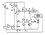
- The accompanying drawing is a schematic diagram of a circuit which incorporates an embodiment of the present invention.
- With reference to the drawing, a load 10 is coupled to a source of electrical power, such as a
first battery 12, by an insulated gate bipolar transistor (IGBT) 13 and a conventional shortcircuit current sensor 11. The emitter of theIGBT 13 is connected to the negative terminal of thefirst battery 12 and the IGBT's collector is connected to the load 10 at a node 38. When the IGBT 13 is turned on, the current from thefirst battery 12 flows through the load 10. - When the current flowing between the load 10 and the
first battery 12 exceeds a given level indicative of a short circuit condition, thecurrent sensor 11 reacts by applying a low logic level signal ontoline 15. Otherwise, a high logic level signal is applied toline 15 by thecurrent sensor 11. - In this circuit, the IGBT 13 enables a relatively low voltage control signal, on the order of ten to twenty volts, to control the application of a relatively high voltage and current to the load, for example, 100 amperes at 550 volts. Specifically, the load 10 is controlled by an input signal at
terminal 14 which is coupled to one input of anAND gate 16. The other input of the AND gate is connected toline 15 from thecurrent sensor 11. Thegate 16 allows a digital logic level signal from an external control circuit to activate theIGBT 13. Specifically, under normal conditions, a high level voltage atterminal 14 turns on the application of electricity to the load, whereas a low level voltage applied to the terminal turns off that electricity. The output of theAND gate 16 is coupled by a current limiting resistor 18 to the base of an NPN transistor Q1. The emitter of transistor Q1 is directly coupled to circuit ground 20, which is connected to the negative terminal of a second battery 22. The second battery 22 supplies a low voltage (e.g. 15 volts) to the IGBT control circuit. The positive terminal of the second battery 22 is connected to apositive voltage bus 24. The collector of transistor Q1 is coupled by a pair of series connectedresistors positive voltage bus 24. - When the output of the
AND gate 16 is high, transistor Q1 turns on reducing the voltage potential at theintermediate node 27 betweenresistors resistors positive voltage bus 24. In this state, approximately 15 volts is applied across this voltage divider to produce an intermediate voltage of approximately +10 volts at asecond node 34 betweenresistors - The
second node 34 is coupled to the bases of a pair of complementary conductivity type transistors Q4 and Q5 connected as an emitter follower between circuit ground 20 and thepositive voltage bus 24. Specifically, the emitters of the complementary transistors Q4 and Q5 are connected together and their collectors are connected to thepositive voltage bus 24 and circuit ground 20, respectively. The magnitude of the voltage appearing at the emitters of transistors Q4 and Q5 corresponds to the magnitude of the voltage applied to their base electrodes which are coupled tonode 34. - The emitters of transistors Q4 and Q5 are coupled by resistor 36 to the gate electrode of the
IGBT 13. Thus, when the voltage atnode 34 is approximately +10 volts, the gate of the IGBT will be driven at about +9.4 volts, which is sufficient to enable theIGBT 13 to conduct several hundred amperes to the load 10. Under normal load conditions, theIGBT 13 will saturate soon after turning on so that the voltage across its collector and emitter Vce will drop to its saturation voltage (approximately 3-5 volts for example) for the applied gate potential. In addition, the potential at the first node 38, between the collector of theIGBT 13 and the load 10, will be equal to the voltage drop across the IGBT. Therefore, first node 38 will be less than the +15 volt level of thepositive voltage bus 24. - In this state, the emitter of transistor Q3, which is coupled across
resistor 30, is pulled up to approximately +15 volts by transistor Q2. As a result, a current flows through transistor Q2, the emitter-base junction of transistor Q3,resistor 40 anddiode 42 to node 38. This current flow causes transistor Q3 to turn on providing a shunt current path aroundresistor 30, raising the potential at thesecond node 34 to about +15 volts. This increase in the voltage at thesecond node 34 raises the potential of the bases of the emitter-follower transistors Q4 and Q5, thereby increasing the IGBT gate drive voltage to approximately +14.4 volts. The higher gate drive voltage increases the conductivity of the IGBT 10 and correspondingly decreases its saturation voltage Vce. The decrease in the saturation voltage of the IGBT decreases the power loss in the device as well as allowing a higher current to flow to the load 10. - Should a short circuit occur across the load 10, the potential at the first node 38 will be substantially equal to the voltage of the first battery 12 (e.g. 550 volts) and significantly higher than the
positive voltage bus 24. In this situation, the IGBT 10 will not saturate when it is turned on. As a result of the potential at the first node 38 being above the positive voltage bus potential, transistor Q3 will not turn on. Therefore, in a short circuit condition,resistor 30 will not be shunted and the potential at the bases of the emitter-follower transistors Q4 and Q5 will remain at their initial bias of approximately +9.4 volts. Consequently, the gate drive voltage and the conductivity of the IGBT 10 will also remain at their initial low levels. If a short circuit occurs after the IGBT 10 has fully turned on, transistor Q3 will be turned off thereby reducing the gate drive voltage and the conductivity of the IGBT. - As noted above, the time interval during which the IGBT 10 can carry a short circuit current, increases as the gate drive voltage decreases. Therefore, in the short circuit condition, the gate drive voltage is reduced enabling the IGBT to withstand the short circuit current for a longer period of time than when it is driven to a higher conductivity level. The precise value of the gate drive voltage in the short circuit condition is chosen so that the IGBT 10 will be able to withstand the short circuit current for a long enough interval for the
current sensor 11 to act. When the current sensor detects a short circuit current, it applies a low logic level toline 15 which forces the output ofgate 16 low. The low level from the gate turns off transistor Q1, which results in theIGBT 13 also turning off.
Claims (7)
an insulated gate bipolar transistor having a gate, an emitter and a collector with the emitter-collector conduction path coupling the load to a source of electricity;
means for sensing the voltage across the collector and emitter of said transistor;
means for driving the gate of said transistor at a first voltage level in response to said means for sensing indicating that the voltage across the collector and emitter is below a given threshold level, or at a second voltage level in response to said means for sensing indicating that the voltage across the collector and emitter is above the given threshold, the first voltage level producing a greater emitter-collector conductivity than the conductivity produced by the second voltage level, wherein the means for driving comprises:
a voltage divider having an intermediate node;
a pair of complementary conductivity type transistors with each transistor having a base, a collector and an emitter, the bases of the pair of transistors being connected to the intermediate node, the emitters of the pair of transistors being connected together and coupled to the gate of the insulated gate bipolar transistor, and the collectors of the pair of transistors being coupled to a voltage source; and
means for altering the voltage divider, in response to said means for sensing the voltage, to vary the voltage at the intermediate node.
means for detecting whether the insulated gate bipolar transistor is in a state of saturation;
means, responsive to said means for detecting, for driving the insulated gate bipolar transistor to a first predefined conductivity level when the insulated gate bipolar transistor is in a state of saturation, or to a second predefined conductivity level when the insulated gate bipolar transistor is not in a state of saturation, the first conductivity level being greater than the second conductivity level.
a voltage divider having an intermediate node;
a pair of complementary conductivity type transistors with each transistor having a base, a collector and an emitter, the bases of the pair of transistors being connected to the intermediate node, the emitters of the pair of transistors being connected together and coupled to the gate of the insulated gate bipolar transistor, and the collectors of the pair of transistors being coupled to a voltage source; and
means for altering the voltage divider, in response to said means for detecting to vary the voltage at the intermediate node.
a source of a voltage potential;
first and second resistors connected in series at a common node;
means for selectively coupling said series connected first and second resistors to said source of a voltage potential;
a pair of complementary conductivity type transistors with each transistor having a base, a collector and an emitter, the bases of the pair of transistors being connected to the common node, the emitters of the pair of transistors being connected together and coupled to the gate of the insulated gate bipolar transistor, and the collectors of the pair of transistors being coupled to said source of a voltage potential;
a shunt transistor having an emitter-collector conduction path connected across one of the first and second resistors, and having a base electrode; and
means for biasing the base of said shunt transistor in response to the voltage across the collector and emitter of the insulated gate bipolar transistor.
Applications Claiming Priority (2)
| Application Number | Priority Date | Filing Date | Title |
|---|---|---|---|
| US336931 | 1989-04-12 | ||
| US07/336,931 US4954917A (en) | 1989-04-12 | 1989-04-12 | Power transistor drive circuit with improved short circuit protection |
Publications (2)
| Publication Number | Publication Date |
|---|---|
| EP0392831A2 true EP0392831A2 (en) | 1990-10-17 |
| EP0392831A3 EP0392831A3 (en) | 1991-12-11 |
Family
ID=23318337
Family Applications (1)
| Application Number | Title | Priority Date | Filing Date |
|---|---|---|---|
| EP19900303925 Withdrawn EP0392831A3 (en) | 1989-04-12 | 1990-04-11 | Power transistor drive circuit with improved short circuit protection |
Country Status (5)
| Country | Link |
|---|---|
| US (1) | US4954917A (en) |
| EP (1) | EP0392831A3 (en) |
| JP (1) | JPH0642179B2 (en) |
| CA (1) | CA1322023C (en) |
| IL (1) | IL93847A0 (en) |
Cited By (2)
| Publication number | Priority date | Publication date | Assignee | Title |
|---|---|---|---|---|
| EP0483744A2 (en) * | 1990-11-02 | 1992-05-06 | Hitachi, Ltd. | Current detection circuit of power semiconductor device and power converter using the circuit |
| FR2700647A1 (en) * | 1993-01-15 | 1994-07-22 | Legrand Sa | Static switch with integrated protection for coupling a load to an electrical source, comprising a bipolar transistor with insulated gate. |
Families Citing this family (19)
| Publication number | Priority date | Publication date | Assignee | Title |
|---|---|---|---|---|
| JP2664735B2 (en) * | 1988-08-26 | 1997-10-22 | 株式会社東芝 | High frequency heating equipment |
| US5192901A (en) * | 1990-03-16 | 1993-03-09 | Cherry Semiconductor Corporation | Short circuit protection |
| JPH0585510A (en) * | 1991-08-07 | 1993-04-06 | Masatake Hirakawa | Packaging method and packaging material for flexible food with decorative picture |
| JP3367699B2 (en) * | 1993-01-08 | 2003-01-14 | 本田技研工業株式会社 | Overcurrent protection circuit |
| US5398148A (en) * | 1993-05-14 | 1995-03-14 | Chrysler Corporation | Protection circuit for high side drivers |
| CA2172890C (en) * | 1995-06-06 | 2005-02-22 | Harold R. Schnetzka | Switch driver circuit |
| US6339526B1 (en) * | 1998-07-01 | 2002-01-15 | Lucent Technologies Inc. | Low voltage cutoff circuit with short circuit detection capability and method of operation thereof |
| JP2003009508A (en) * | 2001-06-19 | 2003-01-10 | Mitsubishi Electric Corp | Power semiconductor device |
| DE10210181C1 (en) * | 2002-03-07 | 2003-07-17 | Semikron Elektronik Gmbh | Overcurrent and over-temperature protection circuit for power semiconductor switch uses diode and positive temperature coefficient resistance in series with latter |
| US6744229B2 (en) * | 2002-03-28 | 2004-06-01 | Sunonwealth Electric Machine Industry Co., Ltd | Safety-guard detective circuit of a fan motor |
| JP4807768B2 (en) * | 2004-06-23 | 2011-11-02 | ルネサスエレクトロニクス株式会社 | Power transistor device and power control system using the same |
| DE102011085657A1 (en) * | 2011-11-03 | 2013-05-08 | Robert Bosch Gmbh | Method and apparatus for operating an electronically commutated electric machine in case of failure |
| CN103973277B (en) | 2013-02-05 | 2017-06-09 | 通用电气公司 | The short-circuit protection circuit and method of insulated gate bipolar transistor |
| US9575113B2 (en) | 2014-02-07 | 2017-02-21 | Infineon Technologies Ag | Insulated-gate bipolar transistor collector-emitter saturation voltage measurement |
| CN105840541B (en) * | 2016-05-04 | 2017-06-06 | 宁波普瑞均胜汽车电子有限公司 | It is a kind of to export the circuit that air blower enables signal |
| JP6885862B2 (en) | 2017-12-28 | 2021-06-16 | ルネサスエレクトロニクス株式会社 | Power converter |
| CN112955846B (en) | 2018-11-02 | 2023-04-21 | 罗姆股份有限公司 | Semiconductor device, relay unit, and vehicle |
| CN117039796A (en) | 2018-11-02 | 2023-11-10 | 罗姆股份有限公司 | Semiconductor unit, semiconductor device, battery unit, and vehicle |
| CN117318683A (en) * | 2023-10-18 | 2023-12-29 | 圣邦微电子(北京)股份有限公司 | Driving circuit, load switching circuit and power supply module of power transistor |
Citations (2)
| Publication number | Priority date | Publication date | Assignee | Title |
|---|---|---|---|---|
| US4095127A (en) * | 1976-03-29 | 1978-06-13 | Rohr Industries, Incorporated | Transistor base drive regulator |
| JPS63177612A (en) * | 1987-01-19 | 1988-07-21 | Toshiba Corp | Gate control circuit |
Family Cites Families (2)
| Publication number | Priority date | Publication date | Assignee | Title |
|---|---|---|---|---|
| US4306270A (en) * | 1978-09-05 | 1981-12-15 | Nartron Corporation | Electrical system monitoring means |
| KR900008276B1 (en) * | 1985-02-08 | 1990-11-10 | 가부시끼가이샤 도시바 | Protection circuit for an insulated gate bipolar transistor utilizing a two-step turn off |
-
1989
- 1989-04-12 US US07/336,931 patent/US4954917A/en not_active Ceased
- 1989-09-28 CA CA000614079A patent/CA1322023C/en not_active Expired - Fee Related
-
1990
- 1990-03-22 IL IL93847A patent/IL93847A0/en not_active IP Right Cessation
- 1990-04-10 JP JP2093265A patent/JPH0642179B2/en not_active Expired - Fee Related
- 1990-04-11 EP EP19900303925 patent/EP0392831A3/en not_active Withdrawn
Patent Citations (2)
| Publication number | Priority date | Publication date | Assignee | Title |
|---|---|---|---|---|
| US4095127A (en) * | 1976-03-29 | 1978-06-13 | Rohr Industries, Incorporated | Transistor base drive regulator |
| JPS63177612A (en) * | 1987-01-19 | 1988-07-21 | Toshiba Corp | Gate control circuit |
Non-Patent Citations (2)
| Title |
|---|
| ELEKTROTECHNISCHE ZEITSCHRIFT - ETZ. vol. 108, no. 19, October 1987, BERLIN DE pages 914 - 920; KEUTER ET AL.: 'Optimierte Ansteuerung heutiger Darlington-Leistungstransistoren ' * |
| PATENT ABSTRACTS OF JAPAN vol. 12, no. 449 (E-686)(3296) November 25, 1988 & JP-A-63 177 612 (TOSHIBA CORP. ) July 21, 1988 * |
Cited By (3)
| Publication number | Priority date | Publication date | Assignee | Title |
|---|---|---|---|---|
| EP0483744A2 (en) * | 1990-11-02 | 1992-05-06 | Hitachi, Ltd. | Current detection circuit of power semiconductor device and power converter using the circuit |
| EP0483744A3 (en) * | 1990-11-02 | 1993-03-17 | Hitachi, Ltd. | Current detection circuit of power semiconductor device and power converter using the circuit |
| FR2700647A1 (en) * | 1993-01-15 | 1994-07-22 | Legrand Sa | Static switch with integrated protection for coupling a load to an electrical source, comprising a bipolar transistor with insulated gate. |
Also Published As
| Publication number | Publication date |
|---|---|
| JPH0317713A (en) | 1991-01-25 |
| EP0392831A3 (en) | 1991-12-11 |
| IL93847A0 (en) | 1990-12-23 |
| US4954917A (en) | 1990-09-04 |
| JPH0642179B2 (en) | 1994-06-01 |
| CA1322023C (en) | 1993-09-07 |
Similar Documents
| Publication | Publication Date | Title |
|---|---|---|
| US4954917A (en) | Power transistor drive circuit with improved short circuit protection | |
| US6275093B1 (en) | IGBT gate drive circuit with short circuit protection | |
| US4885486A (en) | Darlington amplifier with high speed turnoff | |
| US4429339A (en) | AC Transistor switch with overcurrent protection | |
| US5200878A (en) | Drive circuit for current sense igbt | |
| US4949213A (en) | Drive circuit for use with voltage-drive semiconductor device | |
| KR0171713B1 (en) | Overcurrent protection circuit of a power semiconductor transistor | |
| US4117351A (en) | Transistor switching circuit | |
| USRE34107E (en) | Power transistor drive circuit with improved short circuit protection | |
| JP3414859B2 (en) | Turn-off circuit device for overcurrent of semiconductor device | |
| JP3379562B2 (en) | Inverter device | |
| US4023069A (en) | Vertical deflection circuit | |
| JPH08322240A (en) | Method for controlling gate of self-arc-extinguishing semiconductor element | |
| US4572970A (en) | Miller capacitance effect eliminator for use with a push-pull amplifier output stage | |
| JPH0767073B2 (en) | Insulated gate element drive circuit | |
| JP2009095166A (en) | Gate driving device for voltage control type switching device | |
| US3215858A (en) | High speed transistor switching circuit | |
| JP3749109B2 (en) | Power converter | |
| CN215222153U (en) | Semiconductor switch device desaturation detection circuit and motor controller | |
| EP0614278A1 (en) | Drive circuit for use with voltage-driven semiconductor device | |
| GB1165507A (en) | An Improved Electric Motor Braking Circuit | |
| GB2148622A (en) | Electronic control circuit | |
| JP3671796B2 (en) | Drive device for current control element | |
| JP3657676B2 (en) | Switching switching means and bidirectional switching switching means | |
| SU978348A1 (en) | Transistorized switch |
Legal Events
| Date | Code | Title | Description |
|---|---|---|---|
| PUAI | Public reference made under article 153(3) epc to a published international application that has entered the european phase |
Free format text: ORIGINAL CODE: 0009012 |
|
| AK | Designated contracting states |
Kind code of ref document: A2 Designated state(s): DE FR GB NL |
|
| PUAL | Search report despatched |
Free format text: ORIGINAL CODE: 0009013 |
|
| AK | Designated contracting states |
Kind code of ref document: A3 Designated state(s): DE FR GB NL |
|
| 17P | Request for examination filed |
Effective date: 19911220 |
|
| 17Q | First examination report despatched |
Effective date: 19941223 |
|
| STAA | Information on the status of an ep patent application or granted ep patent |
Free format text: STATUS: THE APPLICATION IS DEEMED TO BE WITHDRAWN |
|
| 18D | Application deemed to be withdrawn |
Effective date: 19960418 |