EP0382980A2 - Thermal memory cell and thermal system evaluation - Google Patents
Thermal memory cell and thermal system evaluation Download PDFInfo
- Publication number
- EP0382980A2 EP0382980A2 EP89313457A EP89313457A EP0382980A2 EP 0382980 A2 EP0382980 A2 EP 0382980A2 EP 89313457 A EP89313457 A EP 89313457A EP 89313457 A EP89313457 A EP 89313457A EP 0382980 A2 EP0382980 A2 EP 0382980A2
- Authority
- EP
- European Patent Office
- Prior art keywords
- thermal
- memory cell
- mis
- insulating layer
- capacitor
- Prior art date
- Legal status (The legal status is an assumption and is not a legal conclusion. Google has not performed a legal analysis and makes no representation as to the accuracy of the status listed.)
- Granted
Links
- 238000011156 evaluation Methods 0.000 title claims description 7
- 238000000034 method Methods 0.000 claims abstract description 76
- 239000003990 capacitor Substances 0.000 claims abstract description 50
- 239000000463 material Substances 0.000 claims abstract description 33
- 230000004913 activation Effects 0.000 claims abstract description 30
- 238000007669 thermal treatment Methods 0.000 claims abstract description 28
- 239000004065 semiconductor Substances 0.000 claims abstract description 20
- 239000012212 insulator Substances 0.000 claims abstract description 17
- 229910052751 metal Inorganic materials 0.000 claims abstract description 16
- 239000002184 metal Substances 0.000 claims abstract description 16
- 230000008859 change Effects 0.000 claims abstract description 15
- 239000000969 carrier Substances 0.000 claims abstract description 13
- 150000002500 ions Chemical class 0.000 claims description 22
- VYPSYNLAJGMNEJ-UHFFFAOYSA-N Silicium dioxide Chemical group O=[Si]=O VYPSYNLAJGMNEJ-UHFFFAOYSA-N 0.000 claims description 11
- 239000000758 substrate Substances 0.000 claims description 8
- 239000000377 silicon dioxide Substances 0.000 claims description 5
- 235000012239 silicon dioxide Nutrition 0.000 claims description 5
- 230000004044 response Effects 0.000 claims description 4
- 239000002019 doping agent Substances 0.000 claims description 3
- 229910021421 monocrystalline silicon Inorganic materials 0.000 claims description 3
- 239000000470 constituent Substances 0.000 description 32
- 235000012431 wafers Nutrition 0.000 description 26
- 239000002245 particle Substances 0.000 description 22
- 235000013305 food Nutrition 0.000 description 18
- 239000010408 film Substances 0.000 description 14
- 239000000243 solution Substances 0.000 description 12
- RYGMFSIKBFXOCR-UHFFFAOYSA-N Copper Chemical compound [Cu] RYGMFSIKBFXOCR-UHFFFAOYSA-N 0.000 description 10
- 229910052802 copper Inorganic materials 0.000 description 10
- 239000010949 copper Substances 0.000 description 10
- 238000009792 diffusion process Methods 0.000 description 10
- 230000006870 function Effects 0.000 description 10
- 229910052782 aluminium Inorganic materials 0.000 description 9
- 230000010354 integration Effects 0.000 description 9
- 230000008569 process Effects 0.000 description 9
- XAGFODPZIPBFFR-UHFFFAOYSA-N aluminium Chemical compound [Al] XAGFODPZIPBFFR-UHFFFAOYSA-N 0.000 description 8
- 239000002585 base Substances 0.000 description 7
- 238000010438 heat treatment Methods 0.000 description 7
- 239000012535 impurity Substances 0.000 description 7
- 238000012545 processing Methods 0.000 description 7
- 239000011734 sodium Substances 0.000 description 7
- 238000012546 transfer Methods 0.000 description 7
- DGAQECJNVWCQMB-PUAWFVPOSA-M Ilexoside XXIX Chemical compound C[C@@H]1CC[C@@]2(CC[C@@]3(C(=CC[C@H]4[C@]3(CC[C@@H]5[C@@]4(CC[C@@H](C5(C)C)OS(=O)(=O)[O-])C)C)[C@@H]2[C@]1(C)O)C)C(=O)O[C@H]6[C@@H]([C@H]([C@@H]([C@H](O6)CO)O)O)O.[Na+] DGAQECJNVWCQMB-PUAWFVPOSA-M 0.000 description 6
- 239000012530 fluid Substances 0.000 description 6
- 229910052708 sodium Inorganic materials 0.000 description 6
- XLYOFNOQVPJJNP-UHFFFAOYSA-N water Chemical compound O XLYOFNOQVPJJNP-UHFFFAOYSA-N 0.000 description 6
- 238000006243 chemical reaction Methods 0.000 description 5
- 238000009826 distribution Methods 0.000 description 5
- 230000000694 effects Effects 0.000 description 5
- 229920002120 photoresistant polymer Polymers 0.000 description 5
- WHXSMMKQMYFTQS-UHFFFAOYSA-N Lithium Chemical compound [Li] WHXSMMKQMYFTQS-UHFFFAOYSA-N 0.000 description 4
- XUIMIQQOPSSXEZ-UHFFFAOYSA-N Silicon Chemical compound [Si] XUIMIQQOPSSXEZ-UHFFFAOYSA-N 0.000 description 4
- 239000003822 epoxy resin Substances 0.000 description 4
- 229910052744 lithium Inorganic materials 0.000 description 4
- 229920000647 polyepoxide Polymers 0.000 description 4
- 229910052710 silicon Inorganic materials 0.000 description 4
- 239000010703 silicon Substances 0.000 description 4
- ZLMJMSJWJFRBEC-UHFFFAOYSA-N Potassium Chemical compound [K] ZLMJMSJWJFRBEC-UHFFFAOYSA-N 0.000 description 3
- 150000001450 anions Chemical class 0.000 description 3
- 238000004364 calculation method Methods 0.000 description 3
- 239000008367 deionised water Substances 0.000 description 3
- 229910021641 deionized water Inorganic materials 0.000 description 3
- 230000001419 dependent effect Effects 0.000 description 3
- 238000012417 linear regression Methods 0.000 description 3
- 238000004519 manufacturing process Methods 0.000 description 3
- -1 pharmaceutical Substances 0.000 description 3
- 230000000704 physical effect Effects 0.000 description 3
- 229910052700 potassium Inorganic materials 0.000 description 3
- 239000011591 potassium Substances 0.000 description 3
- 229910000679 solder Inorganic materials 0.000 description 3
- 239000000126 substance Substances 0.000 description 3
- 229910001868 water Inorganic materials 0.000 description 3
- 102000004190 Enzymes Human genes 0.000 description 2
- 108090000790 Enzymes Proteins 0.000 description 2
- CDBYLPFSWZWCQE-UHFFFAOYSA-L Sodium Carbonate Chemical compound [Na+].[Na+].[O-]C([O-])=O CDBYLPFSWZWCQE-UHFFFAOYSA-L 0.000 description 2
- QAOWNCQODCNURD-UHFFFAOYSA-N Sulfuric acid Chemical compound OS(O)(=O)=O QAOWNCQODCNURD-UHFFFAOYSA-N 0.000 description 2
- 230000003044 adaptive effect Effects 0.000 description 2
- 238000004458 analytical method Methods 0.000 description 2
- 150000001768 cations Chemical class 0.000 description 2
- 238000004140 cleaning Methods 0.000 description 2
- 238000013461 design Methods 0.000 description 2
- 238000010586 diagram Methods 0.000 description 2
- 238000005516 engineering process Methods 0.000 description 2
- 230000004907 flux Effects 0.000 description 2
- 230000014509 gene expression Effects 0.000 description 2
- XLYOFNOQVPJJNP-UHFFFAOYSA-M hydroxide Chemical compound [OH-] XLYOFNOQVPJJNP-UHFFFAOYSA-M 0.000 description 2
- 239000007788 liquid Substances 0.000 description 2
- 235000015097 nutrients Nutrition 0.000 description 2
- 239000000523 sample Substances 0.000 description 2
- 239000007787 solid Substances 0.000 description 2
- 230000036962 time dependent Effects 0.000 description 2
- 230000009466 transformation Effects 0.000 description 2
- JBRZTFJDHDCESZ-UHFFFAOYSA-N AsGa Chemical compound [As]#[Ga] JBRZTFJDHDCESZ-UHFFFAOYSA-N 0.000 description 1
- 102000003712 Complement factor B Human genes 0.000 description 1
- 108090000056 Complement factor B Proteins 0.000 description 1
- XPDWGBQVDMORPB-UHFFFAOYSA-N Fluoroform Chemical compound FC(F)F XPDWGBQVDMORPB-UHFFFAOYSA-N 0.000 description 1
- 229910001218 Gallium arsenide Inorganic materials 0.000 description 1
- 244000017020 Ipomoea batatas Species 0.000 description 1
- 235000002678 Ipomoea batatas Nutrition 0.000 description 1
- GRYLNZFGIOXLOG-UHFFFAOYSA-N Nitric acid Chemical compound O[N+]([O-])=O GRYLNZFGIOXLOG-UHFFFAOYSA-N 0.000 description 1
- NBIIXXVUZAFLBC-UHFFFAOYSA-N Phosphoric acid Chemical group OP(O)(O)=O NBIIXXVUZAFLBC-UHFFFAOYSA-N 0.000 description 1
- 229930006000 Sucrose Natural products 0.000 description 1
- CZMRCDWAGMRECN-UGDNZRGBSA-N Sucrose Chemical compound O[C@H]1[C@H](O)[C@@H](CO)O[C@@]1(CO)O[C@@H]1[C@H](O)[C@@H](O)[C@H](O)[C@@H](CO)O1 CZMRCDWAGMRECN-UGDNZRGBSA-N 0.000 description 1
- 125000000218 acetic acid group Chemical group C(C)(=O)* 0.000 description 1
- 239000000654 additive Substances 0.000 description 1
- 230000000996 additive effect Effects 0.000 description 1
- 229910052783 alkali metal Inorganic materials 0.000 description 1
- 150000001340 alkali metals Chemical class 0.000 description 1
- LDDQLRUQCUTJBB-UHFFFAOYSA-N ammonium fluoride Chemical compound [NH4+].[F-] LDDQLRUQCUTJBB-UHFFFAOYSA-N 0.000 description 1
- 230000002547 anomalous effect Effects 0.000 description 1
- 239000007864 aqueous solution Substances 0.000 description 1
- 230000015556 catabolic process Effects 0.000 description 1
- 238000012512 characterization method Methods 0.000 description 1
- 230000002925 chemical effect Effects 0.000 description 1
- 239000004020 conductor Substances 0.000 description 1
- 238000010276 construction Methods 0.000 description 1
- 239000000356 contaminant Substances 0.000 description 1
- 238000010411 cooking Methods 0.000 description 1
- 238000001816 cooling Methods 0.000 description 1
- 238000012937 correction Methods 0.000 description 1
- 235000013365 dairy product Nutrition 0.000 description 1
- 230000006378 damage Effects 0.000 description 1
- 238000006731 degradation reaction Methods 0.000 description 1
- 230000002939 deleterious effect Effects 0.000 description 1
- 238000004925 denaturation Methods 0.000 description 1
- 230000036425 denaturation Effects 0.000 description 1
- 230000008021 deposition Effects 0.000 description 1
- 238000011161 development Methods 0.000 description 1
- 238000007598 dipping method Methods 0.000 description 1
- 229940079593 drug Drugs 0.000 description 1
- 239000003814 drug Substances 0.000 description 1
- 238000001312 dry etching Methods 0.000 description 1
- 239000000975 dye Substances 0.000 description 1
- 235000013601 eggs Nutrition 0.000 description 1
- 150000002148 esters Chemical class 0.000 description 1
- 239000000796 flavoring agent Substances 0.000 description 1
- 235000019634 flavors Nutrition 0.000 description 1
- 238000001879 gelation Methods 0.000 description 1
- 229910052732 germanium Inorganic materials 0.000 description 1
- GNPVGFCGXDBREM-UHFFFAOYSA-N germanium atom Chemical compound [Ge] GNPVGFCGXDBREM-UHFFFAOYSA-N 0.000 description 1
- 150000004820 halides Chemical class 0.000 description 1
- 125000002887 hydroxy group Chemical group [H]O* 0.000 description 1
- 230000002779 inactivation Effects 0.000 description 1
- 238000003780 insertion Methods 0.000 description 1
- 230000037431 insertion Effects 0.000 description 1
- 238000005468 ion implantation Methods 0.000 description 1
- 150000002576 ketones Chemical class 0.000 description 1
- 238000003698 laser cutting Methods 0.000 description 1
- 238000005259 measurement Methods 0.000 description 1
- 229910044991 metal oxide Inorganic materials 0.000 description 1
- 150000004706 metal oxides Chemical class 0.000 description 1
- 230000000813 microbial effect Effects 0.000 description 1
- 238000004377 microelectronic Methods 0.000 description 1
- 235000013336 milk Nutrition 0.000 description 1
- 239000008267 milk Substances 0.000 description 1
- 210000004080 milk Anatomy 0.000 description 1
- 229910017604 nitric acid Inorganic materials 0.000 description 1
- 238000005457 optimization Methods 0.000 description 1
- 230000003647 oxidation Effects 0.000 description 1
- 238000007254 oxidation reaction Methods 0.000 description 1
- TWNQGVIAIRXVLR-UHFFFAOYSA-N oxo(oxoalumanyloxy)alumane Chemical compound O=[Al]O[Al]=O TWNQGVIAIRXVLR-UHFFFAOYSA-N 0.000 description 1
- 238000004806 packaging method and process Methods 0.000 description 1
- 238000009928 pasteurization Methods 0.000 description 1
- 150000002978 peroxides Chemical class 0.000 description 1
- 102000004169 proteins and genes Human genes 0.000 description 1
- 108090000623 proteins and genes Proteins 0.000 description 1
- 230000005855 radiation Effects 0.000 description 1
- 230000009467 reduction Effects 0.000 description 1
- 238000011160 research Methods 0.000 description 1
- 229920005989 resin Polymers 0.000 description 1
- 239000011347 resin Substances 0.000 description 1
- 239000012266 salt solution Substances 0.000 description 1
- 239000000565 sealant Substances 0.000 description 1
- 238000000926 separation method Methods 0.000 description 1
- 229910052814 silicon oxide Inorganic materials 0.000 description 1
- 238000005245 sintering Methods 0.000 description 1
- 229910000029 sodium carbonate Inorganic materials 0.000 description 1
- 238000005476 soldering Methods 0.000 description 1
- 235000014347 soups Nutrition 0.000 description 1
- 238000009987 spinning Methods 0.000 description 1
- 238000003860 storage Methods 0.000 description 1
- 238000006467 substitution reaction Methods 0.000 description 1
- 239000005720 sucrose Substances 0.000 description 1
- 235000000346 sugar Nutrition 0.000 description 1
- 150000008163 sugars Chemical class 0.000 description 1
- 239000008399 tap water Substances 0.000 description 1
- 235000020679 tap water Nutrition 0.000 description 1
- 239000010409 thin film Substances 0.000 description 1
- 235000013343 vitamin Nutrition 0.000 description 1
- 229940088594 vitamin Drugs 0.000 description 1
- 229930003231 vitamin Natural products 0.000 description 1
- 239000011782 vitamin Substances 0.000 description 1
Images


Classifications
-
- G—PHYSICS
- G01—MEASURING; TESTING
- G01K—MEASURING TEMPERATURE; MEASURING QUANTITY OF HEAT; THERMALLY-SENSITIVE ELEMENTS NOT OTHERWISE PROVIDED FOR
- G01K7/00—Measuring temperature based on the use of electric or magnetic elements directly sensitive to heat ; Power supply therefor, e.g. using thermoelectric elements
-
- G—PHYSICS
- G01—MEASURING; TESTING
- G01K—MEASURING TEMPERATURE; MEASURING QUANTITY OF HEAT; THERMALLY-SENSITIVE ELEMENTS NOT OTHERWISE PROVIDED FOR
- G01K3/00—Thermometers giving results other than momentary value of temperature
- G01K3/02—Thermometers giving results other than momentary value of temperature giving means values; giving integrated values
- G01K3/04—Thermometers giving results other than momentary value of temperature giving means values; giving integrated values in respect of time
Definitions
- Thermal processes are used for a broad variety of purposes in the food, chemical, pharmaceutical, and paper and pulp industries.
- such processes include the cooking of canned products such as soup and the pasteurization of dairy products such as milk and eggs.
- thermal processing lines approved by the Food and Drug Administration exist. Because of product changes, five to ten thousand processing lines must be evaluated each year. This procedure is time consuming, expensive, and often inaccurate.
- the Equivalent Point Method differs substantially from previous methods in that all other methods define the thermal treatment based upon a single factor such as enzyme inactivation, microbial destruction, protein denaturation, nutrient loss, etc.
- the problem with these other methods is that a physical and/or chemical effect (flavor, color, product separation and gelation during storage if thermally related) may actually be the shelf life limiting factor.
- Solid-state radiation detectors have been suggested for temperature recording. Such devices are made of a silicon substrate with a layer of lithium diffused into its surface. T. Hirsch, Whither microengineering, Chemtech 118, 121 (February 1986), suggests measuring surface capacitance or resistance in such devices to determine the degree of temperature-dependent lithium migration. G. Haugen and G. Hieftje, An Interdisciplinary Approach to Microinstrumentation, 60 Analytical Chemistry 23A, 27A (1988), suggest that, if several combinations of semiconductor and dopant are used that possess a range of activation energies in such a device, the combination of readouts corresponds to a set of integral equations that can be inverted mathematically (inverse LaPlace transform) to produce the full curve of time versus temperature.
- a new class of thermal history recording devices comprising one or more metal insulator semiconductor (MIS) capacitors.
- the insulating layer is non-uniformly doped with mobile charged carriers.
- At least two MIS capacitors, doped with materials having different activation energies, are exposed to a thermal treatment process, and the change in capacitance in the objects may be employed to calculate the thermal history of the devices.
- Two or more MIS capacitors, each having different activation energies may be mounted in a common support structure to provide a thermal memory cell, which in turn may be embedded in an object (e.g., a food particle) which then undergoes thermal treatment.
- the thermal cells are extremely small, easy and inexpensive to fabricate using well known semiconductor fabrication techniques, and provide an accurate and repeatable integration of the thermal history.
- the thermal cells of the present invention may be used in conjunction with an apparatus for determining the thermal history of the cells.
- the apparatus includes a holder for the cell, a capacitance sensor for detecting changes in the capacitance of each of the MIS capacitors in the cell, and a stored program computer for calculating the thermal history from the detected changes in capacitance.
- the computer may be programmed to efficiently calculate the thermal history of any object which carries two or more thermal calibration materials having different activation energies, be they MIS capacitors or otherwise.
- the equivalent point of a thermal treatment may be calculated by determining the product constituent relationship for each calibration material, interpolating to obtain a range of product constituent relationships versus activation energy and obtaining the equivalent point by applying, for example, a weighted least squares linear regression to the range of product constituent relationships versus activation energy.
- a complete time-temperature profile may be obtained from the product constituent relationships for each calibration material by performing a numerical integration of its product constituent relationships.
- a complete characterization of any thermal process may be obtained.
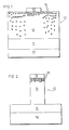
- the capacitor comprises a semiconductor substrate 11, for example, silicon, germanium or gallium arsenide, an insulating layer 12, for example, silicon dioxide or aluminum oxide, formed on the Si substrate, and a conductive layer 13 (preferably aluminum), formed on the insulating layer.
- a second conductive layer 14 (preferably aluminum) is formed under substrate 11.
- substrate 11 is monocrystalline silicon
- insulating layer 12 is a grown silicon dioxide layer 1000 ⁇ thick
- metal electrodes 13 and 14 are typically aluminum electrodes 4000-5000 ⁇ thick.
- the insulating layer 12 is non-uniformly doped with a charged ion 15, with the charged ion preferably being lithium, potassium or sodium.
- any charged ion which is mobile in insulating layer 12 at the expected processing temperatures may be employed.
- the portion of insulator 12 which lies outside top conductor 13 is removed, as shown in Figure 2, so that insulator 12 and the metal layer 13 are coextensive.
- MIS capacitors The theory of MIS capacitors is known in the literature and has been summarized in a detailed paper by Grove, A. et al., Solid-State Electron. 8 , 145 (1965).
- the resultant semiconductor interface boundary layer is either accumulated (conductive) or depleted (dielectric).
- the depletion layer becomes a capacitor in series with that of the insulator. This results in a total capacitance less than the smaller of either of the two components as determined from the product of the two divided by the sum of the two capacitances.
- the diffusion kinetics of the mobile ions can be studied by measuring the resultant characteristic MIS device capacitance-voltage shifts with time at specific temperatures. If the mobile ions are initially attracted to either the metal-insulator or semiconductor-insulator interfaces by a rapid elevated temperature stress under the appropriate bias, the resultant diffusion kinetics at elevated temperatures produce predictable capacitance-voltage (C-V) shifts. According to the invention, such C-V shifts can then be utilized to determine both temperature and time-at-temperature for a particular elevated temperature event.
- C-V capacitance-voltage
- the MIS capacitor structures of the present invention may be fabricated using conventional microelectronic fabrication techniques.
- the MIS capacitor may be fabricated in a semiconductor clean room environment from either high resistivity (preferably greater than 5 ohm cm) n or p-type (100) oriented single crystal Si wafers 11.
- wafers are cleaned by a three-step process to remove organic and inorganic contaminants as well as native oxide surface films.
- This cleaning process was developed by RCA Corp. (see W. Kern, Semiconductor International, April (1984), p. 94) and insures a microscopically clean surface prior to device fabrication.
- wafers 11 are placed in a conventional oxidation tube furnace and thin silicon dioxide films 12, preferably 1000 ⁇ thick, are grown by a dry (O2)/wet (H2O + HCl)/dry (O2) process at 900-1050°C.
- the next step is oxide doping with an aqueous solution of a hydroxide of the desired mobile ion impurity 15.
- aqueous solution of a hydroxide of the desired mobile ion impurity 15 Each wafer is placed on a photoresist spinner and the solution applied while the wafer is spinning at about 2000 rpm. This insures uniformity of film thickness and provides a means of controlling the concentration of the impurity in the oxide film. Alternate means are by solution dipping or ion implantation. The concentration of hydroxide in the water solutions is dependent on the particular mobile ion required in the oxide film for optimal device performance.
- the wafers are then baked on a hot plate at 250°C for one hour to insure adequate impurity diffusion (drive-in) into the thin oxide films. While 250°C is the preferred temperature for the impurities used herein, different temperature ranges may be appropriate for other impurities.
- OH hydroxyl
- halide salt solutions as diffusion sources have been shown to produce considerable anion concentrations in bulk oxide films (E. Yon et al., ibid).
- Such anion-doped oxide films have been predicted by the above authors to retard the rate of diffusion of the mobile cation.
- thin aluminum films 13 (4000-5000 ⁇ ) are vapor deposited on the front sides of the wafers in a high vacuum evaporator system.
- the front side of the wafers are then coated with a 1.5 micron thick layer of positive photoresist, and the wafers hard baked for thirty minutes at 120°-130°C in an oven.
- the wafers are then dipped in a buffered oxide etch solution (ten parts NH4F solution to one part 49% HF solution) to remove back side oxide deposited during the original thermal oxide growth step.
- photoresist films are stripped from the front sides of the wafers with ACCU-STRIPTM (Allied Chemical Co.); then thin films of aluminum 14 (2000 ⁇ or more) are deposited on the back sides of the wafers.
- the wafers are then sintered in 9N2/1H2 forming gas for thirty minutes at 400°C in a tubular diffusion furnace.
- the front sides of the wafers are then recoated with photoresist and the wafers soft baked on a hot plate for five to ten minutes at 95°C.
- the wafers are then aligned, exposed, and developed using an appropriate mask.
- the wafers are hard baked for thirty minutes at 120°-130°C, aluminum etched with twelve parts phosphoric acid/two parts acetic acid/three parts nitric acid solution, and rinsed with deionized water.
- the photoresist is then removed from the wafers with ACCU-STRIPTM and the wafers rinsed with deionized water.
- the portion of field oxide 12 lying outside electrode 13 is removed with a dry etch/liquid etch procedure to avoid lateral etch of the oxide.
- the wafers are placed in a Reactive Ion Etch chamber, a 10 ⁇ 5 Torr or better vacuum drawn, CHF3 gas introduced at 50 x 10 ⁇ 3 Torr, then the wafers are reactive ion etched at 200 watts for up to five minutes. After dry etching, the wafers are etched with buffered oxide etch solution for thirty seconds to remove surface oxide, and rinsed with deionized water.
- wafers are mounted on a vacuum or mechanical chuck and chip dicing performed.
- a high speed circular dicing saw or a laser cutting tool is used to cut chip die with the desired tolerance on chip dimensions.
- 1 mm x 1 mm square die are selected for final device packaging. This saves the steps of photomasking and dry and wet etch.
- each wafer is secured to a vacuum chuck and a measuring probe contacted to the capacitor.
- a capacitance-voltage (C-V) scan is performed with the voltage limits at ⁇ 5 volts.
- the mobile ions are then drawn to the metal/oxide or Si/oxide interface by applying an appropriate bias voltage (positive for n-type and negative for p-type) to the aluminum pad 13 and heating the "thermal/bias stress".
- an appropriate bias voltage positive for n-type and negative for p-type
- -6 volts at 200°C for ten minutes may be used.
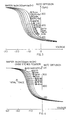
- Figure 3 shows the C-V scan for an MIS capacitor as shown in Figure 1, prepared as described above except that the field oxide outside electrode 13 is not removed.
- the two rightmost lines represent C-V scans after initial thermal/bias stress (1a for five minutes; 1b for ten minutes).
- the remaining lines 2a-2h represent C-V plots taken at half minute intervals during a 160°C thermal treatment. Note the variability between intervals.
- Figure 4 is a series of C-V traces like Figure 3, taken from the same MIS capacitor used to generate Figure 3 except that field oxide lying outside electrode 13 has been substantially removed.
- Rightmost line 2 represents the C-V scan after initial thermal/bias stress.
- the remaining lines 3a-3h represent C-V plots taken at half minute intervals during a 160°C thermal treatment. Note the uniformity between intervals achieved through substantial removal of the field oxide.
- the change in device capacitance with time at a fixed temperature is a much more convenient parameter to measure than is a C-V shift characteristic (Fig. 4). If one applies a fixed bias to a MIS capacitor at a potential in the nearly linear region of the dynamic C-V characteristic, then a predictable time dependent change in device capacitance is evident. This is best illustrated by selecting a bias of -1.0 volts to the p-type device in Fig. 4 and noting the resultant change in the intercept value of a vertical line drawn from the -1.0 volt point (on the abscissa) to the family of C-V shift curves.
- FIG. 5 An example of the dynamic capacitance characteristic of a p-type MIS capacitor with a 1000 ⁇ oxide doped with 200ppm of Na is shown in Fig. 5.
- Time-at-temperature capacitance characteristics are shown at 20°C intervals between 60°C and 120°C for a bias of -0.9 volt.
- Such well behaved capacitance changes with time provides a graded response which permits calculation of equivalent points, time-temperature profiles, and residence times for a thermal treatment, with the algorithms described below.
- the graded response provided according to the present invention is in contrast with prior art temperature sensors which provide an indicator as to whether a predetermined temperature has been reached, but cannot provide information regarding equivalent points or thermal profiles.
- the well behaved capacitance changes provide an integrator of the time/temperature profile. Time-temperature integrators having different activation energies may be provided, according to the present invention, to determine the thermal history of a thermal treatment.
- a Thermal Memory Cell incorporating the MIS capacitors described above is shown in Figures 6-9.
- the cell 20 is comprised of a copper base 21, three MIS capacitor chips 22A-22C, a molded epoxy resin cover 23, and three copper lands 24A-24C on the top of the cover.
- the copper carrier 21 is configured as a rectangle for ease of insertion into solid particles, though other configurations would also be suitable.
- one capacitor 22A is doped with sodium
- one capacitor 22B is doped with potassium
- one capacitor 22C is doped with lithium, to provide capacitors with three different activation energies.
- different activation energies may be provided by doping all the capacitors with sodium, and providing varying levels of positive ions in combination with the sodium.
- one capacitor 22A is doped with Na+ alone
- another capacitor 22B is doped with Na+ and Cl ⁇
- a third capacitor 22 C with Na+ and Br ⁇ .
- Each capacitor chip 22 is positioned in a well formed in the base 21 to align the chip, and the chips 22 are soldered to the base 21 with aluminum saturated tin solder.
- AMCO 64 soldering flux (a product of the American Solder & Flux Co., Inc.) may be employed for all soldered connections in the thermal memory cell.
- the copper lands 24 are etched in place on the epoxy resin cover 23 in the same manner as copper on a printed circuit board. A hole penetrates through the center of each copper land and through the cover. When the epoxy-resin cover is placed over the copper base, each hole is filled with solder 25A-25C so that each capacitor is electrically connected with the copper land positioned thereabove. If desired, the joint between the copper base 21 and the resin cover 23 can be sealed with epoxy resin.
- a serial number or other indicia can be stamped on the bottom surface of the copper carrier 21 so that Thermal Memory Cells in a set of such cells can be distinguished from one another.
- the apparatus 30 is comprised of, in combination, a thermal memory cell holder 31, a capacitance sensor 32, and a thermal history calculator 33.
- the holder 31 may be a vacuum chuck for securing the base of the thermal memory cell 20 ( Figures 6-9) and for making electrical contact to the base 21 thereof, and an electrode mounted on a micromanipulator for making electrical contact to the lands 24 of the cell.
- the mechanical design of such a holder is well known to those having skill in the art, and will be dependent upon the shape and size of the thermal memory cell 20.
- the capacitance sensor 32 may be electrically connected to the cell through the chuck and electrode. Any conventional capacitance sensor, such as a capacitance bridge, may be employed.
- the thermal history calculator 33 is operatively associated with the capacitance sensor. In a preferred embodiment, a stored program microcomputer connected to capacitance sensor 32 can be used.
- Figure 11 illustrates the calculation of equivalent time and temperature and time-temperature profile in the apparatus of Figure 10.
- the flowchart of Figure 11 may be embodied in a stored program which runs on microcomputer 33. This program may be designed according to techniques well known to those having skill in the art, based upon the flowcharts of Figures 11 and 12, and the following description.
- Thermal systems are defined by way of product properties, system properties, and the effect of one on the other.
- the starting point for all thermal system descriptors is the temperature and time exposure.
- Many contact point source temperature methods exist including thermal sensors relating some calibrated change associated with the sensor to a data retrieval system by way of wire connections.
- Other contact sensors use different contacting modes for data retrieval, i.e., electromagnetic waves (visible, infrared, radio waves, etc.).
- Noncontact methods using memory cells
- EPM Equivalent Point Method
- EPM Equivalent Point Method
- M I In (C If /C IO ) where C If is the final concentration of indicator, and C IO is the initial concentration of indicator.
- M C B C e -E C /RT dt
- B C the Arrhenius preexponential factor
- E C the activation energy of the constituent
- M C the relative change in property of the constituent
- M C In (C Cf /C CO ) where C Cf is the final concentration of constituent, and C CO is the initial concentration of constituent.
- the kinetics of the constituent must follow the same order of reaction as the indicator (in this example both were assumed to be first order) for the comparisons to be valid.
- EPM Equivalent Point Method
- the nonlinear regression performs a single regression which allows for both t E and T E directly by using equation 7.
- a Gauss-Marquardt nonlinear regression routine was used, see Press, W. et al., Numerical Recipes: The Art of Scientific Computing (Cambridge University Press, New York, 1986).
- the latter also serves as the heating medium for the particles.
- the functional form of the time-temperature profile of the center of the particle can be determined.
- the equations describing the shape of the time-temperature profile are readily available in most heat transfer textbooks. The parameters that describe the exact curve are now known apriori, however, and must be determined.
- the residence time of a particle in a dynamic system must be known before any predictions can be made regarding the effects of thermal treatment on it. However, this is a very difficult task and, at present, no reliable methods are available that can determine the particle residence time.
- EPM Equivalent Point Method
- the physical properties of the particle and system such as specific heat capacity, density, thermal conductivity, particle size, its initial temperature, and the temperature of the bulk fluid are assumed to be known. Also, from the physics of the system, the shape of the time-temperature profile is known. Since the exact curve is not known, the shape is expressed as in terms of several unknown parameters P1, P2, ..., Pn. These parameters will be determined later and the exact time-temperature profile known (see Figure 11, block 50).
- the method of the present invention uses two or more calibration materials to determine the Equivalent Point (T E , t E ) of the system.
- Use of calibration materials to determine (T E , t E ) of the system are discussed in Sadeghi, F. and Swartzel, K., Calibration Materials for Thermal Systems (Institute of Food Technologists 46th Annual Meeting Food Expo., June 15-18, 1986). In that work calibration materials were used to determine the Equivalent Point of bulk fluid continuous flow systems.
- calibration materials may consist of different mobile ions, such as sodium, potassium, or lithium, each used as a dopant within a thin Metal Insulator Semiconductor (MIS) insulator layer.
- MIS Metal Insulator Semiconductor
- the present method uses the diffusion kinetics of the mobile ion within the oxide layer, the extent of diffusion being dependent on the time-temperature exposure. This extent is determined by measuring the Capacitance Voltage (C-V) shift taking place.
- C-V Capacitance Voltage
- the MIS capacitor is initialized by moving the mobile ions within the oxide to either the metal-oxide or the silicon-oxide interface by elevated temperature stress under a positive or negative bias.
- the initial C-V scan is designated (CV)0.
- CV Capacitance Voltage
- CV Capacitance Voltage
- information relating to the order n, preexponential factor B, and the activation energy E I are also known apriori and recorded. (See Figure 11, block 51 and Figure 12A, block 55).
- the Equivalent Point (t E , T E ) can now be determined (block 63).
- the weighting factor w is set equal to G2 to obtain the best fit (block 63). It should be noted, however, that this is but one of several techniques available to determine the value of the Equivalent Point (t E , T E ).
- the product constituent relationship G can be expressed as The expression inside the integral is evaluated numerically using a procedure such as Gauss Quadrature (see blocks 64, 65 of Figure 12C). This yields a function in terms of the parameters P1, P2, ... P n , which characterize the exact curve, and tF, the residence time of the particle.
- a non-linear regression method such as the Marquardt method can now be used to optimize the parameters, using the table of G versus E values obtained above. Details of the procedure and a sample problem with its output are presented below.
- the G-values are evaluated by numerical integration.
- any numerical integration routine can be used; however, Gauss Quadrature and Romberg integration routines require less computational effort than other routines like Simpson rule, trapezoidal rule, etc.
- the Adaptive Gauss Quadrature can be used. See Forsythe, G. et al., "Computer Methods for Mathematical Computations” (Prentice Hall, New Jersey, 1977).
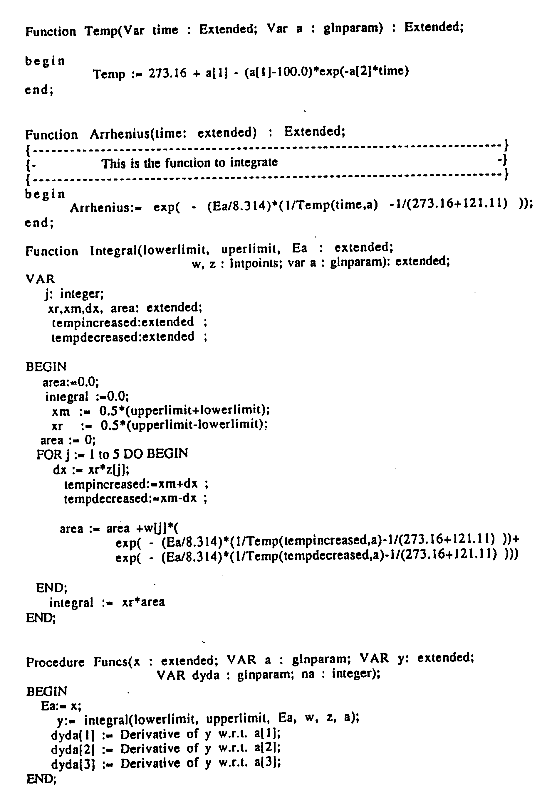
- Function Temp is the only part of the program that has to be changed to introduce any time-temperature profile including any number of parameters. However, in addition to empirical models, those models based upon transport phenomena and physics may be appropriate resulting in parameters related to physico-chemical properties.
- Function Arrhenius introduces the typical exponential transformation for the temperature (Temp) where the activation energy (Ea) is a parameter.
- Function Integral evaluates G-values using a 10-point Gauss Quadrature procedure.
- the residence time of a single particle is known from the procedure described above.
- the residence time distribution (RTD) of particles through a system can be measured by extending the same procedure for a system containing particulates, some or all of which contain a memory cell (MC) in the center. A complete RTD would then be available from the data.
- MC memory cell
- ⁇ thermal diffusivity
- t time
- R particle radius
- the surface temperature can be calculated by using the same procedure described above to determine the temperature profile. This measurement can be then used to confirm/verify the accuracy of the method used to determine the heat transfer coefficient, h.
- the EPM can also be used to evaluate several thermodynamic properties. In addition, it can be used to predict constituent kinetics in microenvironments and fouling dynamics of heat exchangers.
- 20% sucrose solution acidified with sulfuric acid to pH 2.5, and blue #2 solution buffered with sodium carbonate to pH 11.3 are used as thermal constituents and encapsulated in 1/4" O.D. cylindrical aluminum modules.
- the ends of the modules are sealed with silicon sealant (heat resistant and stable up to 400°C).
- the thermal constituents are placed in the modules with a hypodermic syringe.
- the two modules containing different thermal constituents are placed at the center of cans filled with sweet potato and water and the cans sealed.
- the cans are thermally treated at between 110-125°C (230-256°F) in a batch retort. After heating, the cans are cooled by tap water and the solutions inside the modules recovered and diluted to 1 milliliter. Constituent changes occurring in each individual module is assayed and the equivalent point for the thermal treatment calculated by essentially the same procedures as described above.
Landscapes
- Physics & Mathematics (AREA)
- General Physics & Mathematics (AREA)
- Investigating Or Analyzing Materials By The Use Of Electric Means (AREA)
- Investigating Or Analyzing Materials Using Thermal Means (AREA)
- Testing Or Measuring Of Semiconductors Or The Like (AREA)
- Semiconductor Integrated Circuits (AREA)
- Semiconductor Memories (AREA)
Abstract
Description
- Thermal processes are used for a broad variety of purposes in the food, chemical, pharmaceutical, and paper and pulp industries. In the food processing industry, such processes include the cooking of canned products such as soup and the pasteurization of dairy products such as milk and eggs. At present, more than seventy thousand thermal processing lines approved by the Food and Drug Administration exist. Because of product changes, five to ten thousand processing lines must be evaluated each year. This procedure is time consuming, expensive, and often inaccurate.
- In many industries, it is desirable to know the thermal history of particulates suspended in a liquid as they travel through a thermal processing apparatus. Due to the complex nature of these systems, however, true thermal histories cannot be obtained.
- Procedures for use of the Equivalent Point Method (EPM) for analyzing the thermal effects on products during continuous flow heating have been disclosed. See K. Swartzel, 47 J. Food Sci. 1886 (1982); K. Swartzel, 34 J. Agric. Food Chem. 397 (1986). The Equivalent Point Method differs substantially from previous methods in that all other methods define the thermal treatment based upon a single factor such as enzyme inactivation, microbial destruction, protein denaturation, nutrient loss, etc. The problem with these other methods is that a physical and/or chemical effect (flavor, color, product separation and gelation during storage if thermally related) may actually be the shelf life limiting factor.
- Calibration materials useful in the equivalent point method are discussed in F. Sadeghi and K. Swartzel, Calibration Materials for Thermal Systems (Institute of Food Technologists 46th Annual Meeting Food Expo, June 15-18, 1986) (tape available from Institute of Food Technologists). Candidate calibration materials mentioned are esters, ketones, peroxides, sugars, vitamins, enzymes and dyes.
- Solid-state radiation detectors have been suggested for temperature recording. Such devices are made of a silicon substrate with a layer of lithium diffused into its surface. T. Hirsch, Whither microengineering, Chemtech 118, 121 (February 1986), suggests measuring surface capacitance or resistance in such devices to determine the degree of temperature-dependent lithium migration. G. Haugen and G. Hieftje, An Interdisciplinary Approach to Microinstrumentation, 60 Analytical Chemistry 23A, 27A (1988), suggest that, if several combinations of semiconductor and dopant are used that possess a range of activation energies in such a device, the combination of readouts corresponds to a set of integral equations that can be inverted mathematically (inverse LaPlace transform) to produce the full curve of time versus temperature.
- The disadvantages of existing technology for thermal system evaluation pose severe problems for the Food Processing Industry. There is presently a critical need to accurately characterize thermal behavior within a food particle as it is pumped through a continuous flow thermal processing apparatus. The present invention is based on our continued research in this area.
- According to the invention, a new class of thermal history recording devices comprising one or more metal insulator semiconductor (MIS) capacitors are provided. The insulating layer is non-uniformly doped with mobile charged carriers. At least two MIS capacitors, doped with materials having different activation energies, are exposed to a thermal treatment process, and the change in capacitance in the objects may be employed to calculate the thermal history of the devices. Two or more MIS capacitors, each having different activation energies, may be mounted in a common support structure to provide a thermal memory cell, which in turn may be embedded in an object (e.g., a food particle) which then undergoes thermal treatment. The thermal cells are extremely small, easy and inexpensive to fabricate using well known semiconductor fabrication techniques, and provide an accurate and repeatable integration of the thermal history.
- The thermal cells of the present invention may be used in conjunction with an apparatus for determining the thermal history of the cells. The apparatus includes a holder for the cell, a capacitance sensor for detecting changes in the capacitance of each of the MIS capacitors in the cell, and a stored program computer for calculating the thermal history from the detected changes in capacitance.
- According to the invention, the computer may be programmed to efficiently calculate the thermal history of any object which carries two or more thermal calibration materials having different activation energies, be they MIS capacitors or otherwise. The equivalent point of a thermal treatment may be calculated by determining the product constituent relationship for each calibration material, interpolating to obtain a range of product constituent relationships versus activation energy and obtaining the equivalent point by applying, for example, a weighted least squares linear regression to the range of product constituent relationships versus activation energy. A complete time-temperature profile may be obtained from the product constituent relationships for each calibration material by performing a numerical integration of its product constituent relationships. A complete characterization of any thermal process may be obtained.
- In the drawings:
- Figure 1 is a cross-sectional view of a MIS capacitor after initial thermal/bias stress, with the field oxide present;
- Figure 2 is a cross-sectional view of a MIS capacitor after initial thermal/bias stress, with the field oxide removed;
- Figure 3 is a plot of capacitance against voltage shift for a MIS capacitor as shown in Figure 1 after different thermal treatments;
- Figure 4 is a plot of capacitance against voltage shift for a MIS capacitor as shown in Figure 2 after different thermal treatments;
- Figure 5 is a plot of capacitance over time at various temperatures for a device as shown in Figure 2;
- Figure 6 is a top plan view of a thermal memory cell of the present invention with the cover removed;
- Figure 7 is a cross-sectional view of the thermal memory cell shown in Figure 6;
- Figure 8 is a top plan view of a thermal memory cell of the present invention with the cover in place;
- Figure 9 is a cross-sectional view of the thermal memory cell shown in Figure 8;
- Figure 10 is a schematic wiring diagram of an apparatus according to the present invention;
- Figure 11 is a simplified flowchart illustrating certain operations for computing equivalent times and temperatures and time-temperature profiles according to the present invention; and
- Figures 12A-12C are simplified flowcharts illustrating the details of certain operations of Figure 11.
- A
single MIS capacitor 10, as prepared for use in the present invention, is shown in Figures 1 and 2. The capacitor comprises asemiconductor substrate 11, for example, silicon, germanium or gallium arsenide, aninsulating layer 12, for example, silicon dioxide or aluminum oxide, formed on the Si substrate, and a conductive layer 13 (preferably aluminum), formed on the insulating layer. A second conductive layer 14 (preferably aluminum) is formed undersubstrate 11. In a preferred embodiment,substrate 11 is monocrystalline silicon,insulating layer 12 is a grown silicon dioxide layer 1000 Å thick, whilemetal electrodes insulating layer 12 is non-uniformly doped with acharged ion 15, with the charged ion preferably being lithium, potassium or sodium. However, it will be understood by those having skill in the art that any charged ion which is mobile in insulatinglayer 12 at the expected processing temperatures may be employed. Preferably, the portion ofinsulator 12 which lies outsidetop conductor 13 is removed, as shown in Figure 2, so thatinsulator 12 and themetal layer 13 are coextensive. - The theory of MIS capacitors is known in the literature and has been summarized in a detailed paper by Grove, A. et al., Solid-State Electron. 8, 145 (1965). Depending upon whether the metal electrode is biased positively or negatively for a given semiconductor type (p or n type), the resultant semiconductor interface boundary layer is either accumulated (conductive) or depleted (dielectric). In the latter case, the depletion layer becomes a capacitor in series with that of the insulator. This results in a total capacitance less than the smaller of either of the two components as determined from the product of the two divided by the sum of the two capacitances.
- Introduction of mobile ionized impurities (dopants) such as the alkali metals Na⁺, K⁺ and Li⁺ into the insulating layer of the MIS structure has been shown to produce time-dependent shifts in the normal capacitance-voltage characteristic of the device at elevated temperatures [see Kerr, D., IBM Journal 8, 376 (1964); Snow, E. et al., J. Appl. Phys. 36, 1664 (1965); Yon, E. et al., IEEE Trans. Electron Devices ED-13, 276 (1966); Antyushin, V. et al., Physica Status Solidi (a) 56, K91 (1979); Yamashita, K. et al., J. Appl. Phys. 20, 1429 (1981); and Hillen, M. and Verwey, J., 1 Instabilities in Silicon Devices, Chap. 8 (G. Barbottin and A. Vapaille, eds., North Holland Book Co., Amsterdam, 1986)]. The presence of such mobile ions is normally undesirable in semiconductor device structures since it can produce anomalous device surface leakage paths that are deleterious to device operation [see Grove, A., Physics and Technology of Semiconductor Devices, Chap. 12 (John Wiley and Sons, New York, 1967), and Sze, S., Physics of Semiconductor Devices, Chap. 10 (Wiley-Interscience Publ. Co., New York, 1969)].
- According to the invention, when controlled amounts of certain mobile ion impurities are non-uniformly introduced into the insulator of a MIS capacitor, the diffusion kinetics of the mobile ions can be studied by measuring the resultant characteristic MIS device capacitance-voltage shifts with time at specific temperatures. If the mobile ions are initially attracted to either the metal-insulator or semiconductor-insulator interfaces by a rapid elevated temperature stress under the appropriate bias, the resultant diffusion kinetics at elevated temperatures produce predictable capacitance-voltage (C-V) shifts. According to the invention, such C-V shifts can then be utilized to determine both temperature and time-at-temperature for a particular elevated temperature event.
- The MIS capacitor structures of the present invention may be fabricated using conventional microelectronic fabrication techniques. For example, the MIS capacitor may be fabricated in a semiconductor clean room environment from either high resistivity (preferably greater than 5 ohm cm) n or p-type (100) oriented single
crystal Si wafers 11. - Initially, wafers are cleaned by a three-step process to remove organic and inorganic contaminants as well as native oxide surface films. This cleaning process was developed by RCA Corp. (see W. Kern, Semiconductor International, April (1984), p. 94) and insures a microscopically clean surface prior to device fabrication.
- After surface cleaning,
wafers 11 are placed in a conventional oxidation tube furnace and thinsilicon dioxide films 12, preferably 1000 Å thick, are grown by a dry (O₂)/wet (H₂O + HCl)/dry (O₂) process at 900-1050°C. - The next step is oxide doping with an aqueous solution of a hydroxide of the desired
mobile ion impurity 15. Each wafer is placed on a photoresist spinner and the solution applied while the wafer is spinning at about 2000 rpm. This insures uniformity of film thickness and provides a means of controlling the concentration of the impurity in the oxide film. Alternate means are by solution dipping or ion implantation. The concentration of hydroxide in the water solutions is dependent on the particular mobile ion required in the oxide film for optimal device performance. - After deposition of the doping solution on device wafer surfaces, the wafers are then baked on a hot plate at 250°C for one hour to insure adequate impurity diffusion (drive-in) into the thin oxide films. While 250°C is the preferred temperature for the impurities used herein, different temperature ranges may be appropriate for other impurities. From the literature limited diffusivity of the hydroxyl (OH) anion is evident in silicon dioxide films (E. Yon et al., IEEE Trans. on Electron Devices ED-13, 276 (1966)); hence, unpredictable anion effects upon mobile cation diffusion in oxide films are minimized. In contrast, the use of halide salt solutions as diffusion sources have been shown to produce considerable anion concentrations in bulk oxide films (E. Yon et al., ibid). Such anion-doped oxide films have been predicted by the above authors to retard the rate of diffusion of the mobile cation.
- Next, thin aluminum films 13 (4000-5000 Å) are vapor deposited on the front sides of the wafers in a high vacuum evaporator system. The front side of the wafers are then coated with a 1.5 micron thick layer of positive photoresist, and the wafers hard baked for thirty minutes at 120°-130°C in an oven. The wafers are then dipped in a buffered oxide etch solution (ten parts NH₄F solution to one part 49% HF solution) to remove back side oxide deposited during the original thermal oxide growth step. Afterward, photoresist films are stripped from the front sides of the wafers with ACCU-STRIP™ (Allied Chemical Co.); then thin films of aluminum 14 (2000 Å or more) are deposited on the back sides of the wafers. The wafers are then sintered in 9N₂/1H₂ forming gas for thirty minutes at 400°C in a tubular diffusion furnace.
- To create appropriate surface electrode patterns, the front sides of the wafers are then recoated with photoresist and the wafers soft baked on a hot plate for five to ten minutes at 95°C. The wafers are then aligned, exposed, and developed using an appropriate mask. Next, the wafers are hard baked for thirty minutes at 120°-130°C, aluminum etched with twelve parts phosphoric acid/two parts acetic acid/three parts nitric acid solution, and rinsed with deionized water. The photoresist is then removed from the wafers with ACCU-STRIP™ and the wafers rinsed with deionized water.
- Finally, the portion of
field oxide 12 lying outsideelectrode 13 is removed with a dry etch/liquid etch procedure to avoid lateral etch of the oxide. The wafers are placed in a Reactive Ion Etch chamber, a 10⁻⁵ Torr or better vacuum drawn, CHF₃ gas introduced at 50 x 10⁻³ Torr, then the wafers are reactive ion etched at 200 watts for up to five minutes. After dry etching, the wafers are etched with buffered oxide etch solution for thirty seconds to remove surface oxide, and rinsed with deionized water. - In the alternative, after sintering, wafers are mounted on a vacuum or mechanical chuck and chip dicing performed. For this operation, either a high speed circular dicing saw or a laser cutting tool is used to cut chip die with the desired tolerance on chip dimensions. For the proposed application, 1 mm x 1 mm square die are selected for final device packaging. This saves the steps of photomasking and dry and wet etch.
- After MIS capacitor construction is completed, each wafer is secured to a vacuum chuck and a measuring probe contacted to the capacitor. A capacitance-voltage (C-V) scan is performed with the voltage limits at ±5 volts. The mobile ions are then drawn to the metal/oxide or Si/oxide interface by applying an appropriate bias voltage (positive for n-type and negative for p-type) to the
aluminum pad 13 and heating the "thermal/bias stress". For p-type wafers, -6 volts at 200°C for ten minutes may be used. - Figure 3 shows the C-V scan for an MIS capacitor as shown in Figure 1, prepared as described above except that the field oxide outside
electrode 13 is not removed. The two rightmost lines represent C-V scans after initial thermal/bias stress (1a for five minutes; 1b for ten minutes). The remaining lines 2a-2h represent C-V plots taken at half minute intervals during a 160°C thermal treatment. Note the variability between intervals. - Figure 4 is a series of C-V traces like Figure 3, taken from the same MIS capacitor used to generate Figure 3 except that field oxide lying outside
electrode 13 has been substantially removed. Rightmost line 2 represents the C-V scan after initial thermal/bias stress. The remaining lines 3a-3h represent C-V plots taken at half minute intervals during a 160°C thermal treatment. Note the uniformity between intervals achieved through substantial removal of the field oxide. - For many thermal memory cell applications, the change in device capacitance with time at a fixed temperature is a much more convenient parameter to measure than is a C-V shift characteristic (Fig. 4). If one applies a fixed bias to a MIS capacitor at a potential in the nearly linear region of the dynamic C-V characteristic, then a predictable time dependent change in device capacitance is evident. This is best illustrated by selecting a bias of -1.0 volts to the p-type device in Fig. 4 and noting the resultant change in the intercept value of a vertical line drawn from the -1.0 volt point (on the abscissa) to the family of C-V shift curves.
- An example of the dynamic capacitance characteristic of a p-type MIS capacitor with a 1000 Å oxide doped with 200ppm of Na is shown in Fig. 5. Time-at-temperature capacitance characteristics are shown at 20°C intervals between 60°C and 120°C for a bias of -0.9 volt. Such well behaved capacitance changes with time provides a graded response which permits calculation of equivalent points, time-temperature profiles, and residence times for a thermal treatment, with the algorithms described below. The graded response provided according to the present invention is in contrast with prior art temperature sensors which provide an indicator as to whether a predetermined temperature has been reached, but cannot provide information regarding equivalent points or thermal profiles. Stated another way, the well behaved capacitance changes provide an integrator of the time/temperature profile. Time-temperature integrators having different activation energies may be provided, according to the present invention, to determine the thermal history of a thermal treatment.
- A Thermal Memory Cell incorporating the MIS capacitors described above is shown in Figures 6-9. The
cell 20 is comprised of acopper base 21, threeMIS capacitor chips 22A-22C, a moldedepoxy resin cover 23, and threecopper lands 24A-24C on the top of the cover. Thecopper carrier 21 is configured as a rectangle for ease of insertion into solid particles, though other configurations would also be suitable. In one embodiment, onecapacitor 22A is doped with sodium, onecapacitor 22B is doped with potassium, and onecapacitor 22C is doped with lithium, to provide capacitors with three different activation energies. Alternatively, different activation energies may be provided by doping all the capacitors with sodium, and providing varying levels of positive ions in combination with the sodium. It has been found that different activation energies for sodium or other positive ions may be provided by doping with negative ions such as Cl⁻ or Br⁻. Thus, in another embodiment, onecapacitor 22A is doped with Na⁺ alone, anothercapacitor 22B is doped with Na⁺ and Cl⁻ and athird capacitor 22 C with Na⁺ and Br⁻. - Each capacitor chip 22 is positioned in a well formed in the base 21 to align the chip, and the chips 22 are soldered to the base 21 with aluminum saturated tin solder.
AMCO 64 soldering flux (a product of the American Solder & Flux Co., Inc.) may be employed for all soldered connections in the thermal memory cell. The copper lands 24 are etched in place on theepoxy resin cover 23 in the same manner as copper on a printed circuit board. A hole penetrates through the center of each copper land and through the cover. When the epoxy-resin cover is placed over the copper base, each hole is filled withsolder 25A-25C so that each capacitor is electrically connected with the copper land positioned thereabove. If desired, the joint between thecopper base 21 and theresin cover 23 can be sealed with epoxy resin. A serial number or other indicia can be stamped on the bottom surface of thecopper carrier 21 so that Thermal Memory Cells in a set of such cells can be distinguished from one another. - A simplified block diagram of an apparatus for determining the thermal history of a thermal process according to the present invention is illustrated in Figure 10. The apparatus 30 is comprised of, in combination, a thermal
memory cell holder 31, acapacitance sensor 32, and athermal history calculator 33. Theholder 31 may be a vacuum chuck for securing the base of the thermal memory cell 20 (Figures 6-9) and for making electrical contact to thebase 21 thereof, and an electrode mounted on a micromanipulator for making electrical contact to thelands 24 of the cell. The mechanical design of such a holder is well known to those having skill in the art, and will be dependent upon the shape and size of thethermal memory cell 20. Thecapacitance sensor 32 may be electrically connected to the cell through the chuck and electrode. Any conventional capacitance sensor, such as a capacitance bridge, may be employed. Thethermal history calculator 33 is operatively associated with the capacitance sensor. In a preferred embodiment, a stored program microcomputer connected tocapacitance sensor 32 can be used. - Figure 11 illustrates the calculation of equivalent time and temperature and time-temperature profile in the apparatus of Figure 10. In a preferred embodiment, the flowchart of Figure 11 may be embodied in a stored program which runs on
microcomputer 33. This program may be designed according to techniques well known to those having skill in the art, based upon the flowcharts of Figures 11 and 12, and the following description. - Thermal systems are defined by way of product properties, system properties, and the effect of one on the other. The starting point for all thermal system descriptors is the temperature and time exposure. Many contact point source temperature methods exist including thermal sensors relating some calibrated change associated with the sensor to a data retrieval system by way of wire connections. Other contact sensors use different contacting modes for data retrieval, i.e., electromagnetic waves (visible, infrared, radio waves, etc.). Noncontact methods (using memory cells) have only recently become commercially available with limited application due to the current state of the technology. With the development of the Equivalent Point Method (EPM) of thermal evaluation, numerous new methods for determining product and system responses to heat are now available.
- The key concept behind the Equivalent Point Method (EPM) is that any system, however complex, can be thermally characterized by two parameters, namely the Equivalent temperature, TE, and the Equivalent time, tE. These two parameters uniquely define the system and hence can be used to compare the changes undergone by different constituents when subject to the same thermal treatment. For example, two chemical constituents with different kinetic properties will undergo different extents of thermal degradation when subject to the same thermal environment. However, both constituents will possess the same equivalent time, tE, and temperature, TE. The Equivalent Point Method (tE, TE) is hence a property of the system and is independent of the kinetic parameters (Order, n; Activation Energy, E; preexponential factor, B; etc.) of the individual constituents.
- Other time-temperature indicators available commercially match the activation energy of the indicator with the desired constituent and assume that the change in the indicator corresponds to the change in the constituent. Suppose the kinetics of an indicator were given by the general equation
(1) MI = BI e-E I /RT dt
where EI is the activation energy of the indicator, BI is the Arrhenius preexponential factor, and MI is the relative change in property of indicator (concentration, color, nutrient loss, etc.) - In the indicator that follows first order kinetics, then
(2) MI = In (CIf/CIO)
where CIf is the final concentration of indicator, and CIO is the initial concentration of indicator. - The kinetics of a constituent can be given by
(3) MC = BC e-E C /RT dt
where BC is the Arrhenius preexponential factor, EC is the activation energy of the constituent, and MC is the relative change in property of the constituent. - If the constituent also follows first order reaction kinetics, then
(4) MC = In (CCf/CCO)
where CCf is the final concentration of constituent, and CCO is the initial concentration of constituent. - It can be seen from equations (1) and (3) that if the activation energy of the indicator EI is matched to equal the activation energy of the constituent, EC, then the expressions inside the integral in both equations would be equal. However, unless the preexponential factor of the indicator (BI) is also equal to that of the constituent (BC), the relative change in property of the indicator (MI); would not be the same as that of the constituent (MC).
- In addition, the kinetics of the constituent must follow the same order of reaction as the indicator (in this example both were assumed to be first order) for the comparisons to be valid.
- Hence, it is seen that merely matching the activation energies of the indicator and constituent is not sufficient and will lead to erroneous conclusions regarding the final concentration predicted for the constituent (CF). The Equivalent Point Method (EPM) as described in detail below, matches the equivalences of the system rather than the activation energies or other properties of the individual constituents, and is thus not prone to the same errors as the other available methods.
- The Equivalent Point Method (EPM) of thermal evaluation was originally developed for use with first order reactions to compare direct and indirect aseptic heating systems, Swartzel, K., J. Food Sci. 47, 186 (1982). It was later extended to include reactions which were not first order, Swartzel, K. and Jones, V., 1984. At present, however, only one procedure (Line Intersections method) has been described in the literature to determine both tE and TE, see Sadeghi, F. et al., J. Food Proc. and Pres. 10, 331 (1986), and Swartzel, K., J. Food Sci. 47, 186 (1982). According to the invention, a new method for calculating the equivalent point method is described.
- A critical step in determining both tE and TE for a known time-temperature distribution, T(t), is the integration of the Arrhenius equation. This integration for different activation energies result in the thermal reduction relationship, G-value, see Swartzel, K., J. Food Sci. 47, 186 (1982) and Swartzel, K., J. Food Sci. 49, 803 (1984). Integration of the rate law equation with substitution of the Arrhenius model for the rate constant yields an absolute G-value:



- Usually, thermal treatments are divided into three sections: heating, holding, and cooling. Before parameter estimation, the contribution of the different thermal sections has to be evaluated. Therefore, for a selected Ea-value, a G-value is calculated for each portion of the thermal curve. G-values for the different portions are summed because thermal effects are additive. For any particular value of Ea, equation (8) yields:
(10) GTotal = GHeat + GHold + GCool
The equivalent time (tE) and equivalent temperature (TE) are obtained from the following model:
- The following three methods for estimating the equivalent point can be used:
- This method has been reported in the literature. See Swartzel, K., J. Food Sci. 47, 186 (1982); Swartzel, K., J. Food Sci. 49, 803 (1984); and Sadeghi, F. et al., J. Food Proc. and Pres. 10, 331 (1986).
- The nonlinear regression performs a single regression which allows for both tE and TE directly by using equation 7. A Gauss-Marquardt nonlinear regression routine was used, see Press, W. et al., Numerical Recipes: The Art of Scientific Computing (Cambridge University Press, New York, 1986).
- The linear least squares analysis presented above assume that the variance is constant throughout the range of measured values. If this is not the case, weighted least squares allows for a better parameter estimation. In addition, parameter estimation involving exponents requires weighted least squares, as shown by Norris, A., Computational Chemistry an Introduction to Numerical Methods (J. Wiley & Sons, New York, 1981). This method requires the determination of slope and intercept of the transformed
equation 13. For a semilog transformation, the weighting function is the square of the independent variable. Therefore, the function to be minimized is:
- Using the EPM a variety of memory cell designs allows the determination of the following thermal information:
- (a) Actual time-temperature history of a point source within a thermal system, including dynamic systems.
- (b) The residence time of the point in a dynamic system.
- (c) The residence time distribution (RTD) of particles moving in a fluid in a dynamic thermal system.
- (d) The film side heat transfer coefficient as a particle - fluid boundary in a dynamic thermal system.
- (e) Constituent kinetics in micro-environments at point sources in dynamic systems.
- (f) Thermodynamic and transport properties of materials such as specific heat capacity, thermal conductivity, thermal diffusivity, enthalpy, entropy, internal energy, etc., in dynamic systems.
- (g) Fouling dynamics of heat exchangers.
- In a typical thermal system consisting of particles moving in a carrier fluid, the latter also serves as the heating medium for the particles. Assuming that the physical properties of the particle such as specific heat capacity, thermal conductivity, size, and density are known, the functional form of the time-temperature profile of the center of the particle can be determined. The equations describing the shape of the time-temperature profile are readily available in most heat transfer textbooks. The parameters that describe the exact curve are now known apriori, however, and must be determined.
- The residence time of a particle in a dynamic system must be known before any predictions can be made regarding the effects of thermal treatment on it. However, this is a very difficult task and, at present, no reliable methods are available that can determine the particle residence time.
- The Equivalent Point Method (EPM) allows for evaluating the exact time-temperature profile of the particle center, and the residence time of a particle in a dynamic system.
- The physical properties of the particle and system such as specific heat capacity, density, thermal conductivity, particle size, its initial temperature, and the temperature of the bulk fluid are assumed to be known. Also, from the physics of the system, the shape of the time-temperature profile is known. Since the exact curve is not known, the shape is expressed as in terms of several unknown parameters P1, P2, ..., Pn. These parameters will be determined later and the exact time-temperature profile known (see Figure 11, block 50).
- The method of the present invention uses two or more calibration materials to determine the Equivalent Point (TE, tE) of the system. Use of calibration materials to determine (TE, tE) of the system are discussed in Sadeghi, F. and Swartzel, K., Calibration Materials for Thermal Systems (Institute of Food Technologists 46th Annual Meeting Food Expo., June 15-18, 1986). In that work calibration materials were used to determine the Equivalent Point of bulk fluid continuous flow systems. In the present case, calibration materials may consist of different mobile ions, such as sodium, potassium, or lithium, each used as a dopant within a thin Metal Insulator Semiconductor (MIS) insulator layer. As discussed earlier in the detailed description of the MIS capacitor, the device is small enough to be inserted into the center of the particle undergoing thermal treatment, yielding a point source Equivalent Point available for other system thermal determinations.
- The present method uses the diffusion kinetics of the mobile ion within the oxide layer, the extent of diffusion being dependent on the time-temperature exposure. This extent is determined by measuring the Capacitance Voltage (C-V) shift taking place. The MIS capacitor is initialized by moving the mobile ions within the oxide to either the metal-oxide or the silicon-oxide interface by elevated temperature stress under a positive or negative bias. The initial C-V scan is designated (CV)₀. After the device is subject to a time-temperature profile, another C-V scan is done to measure the extent of this shift. This is designated (CV)f. In addition, information relating to the order n, preexponential factor B, and the activation energy EI are also known apriori and recorded. (See Figure 11, block 51 and Figure 12A, block 55).
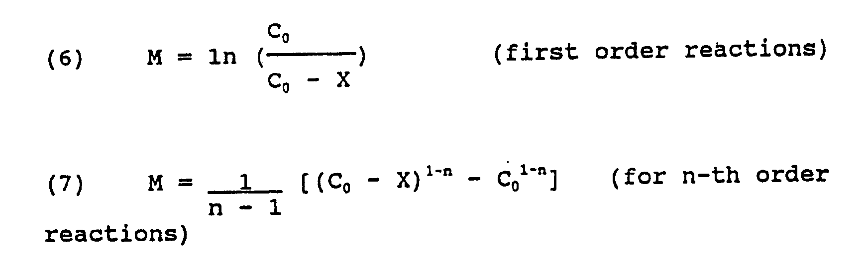
- Referring now to Figure 12A, if the diffusion is first order (n = 1) (block 57), then the relative change in C-V shift M₁ is given by
(13) MI = In (CV)f/(CV)₀
(block 59) where B is the preexponential factor, E is the activation energy, tf is the final time or residence time of particle, and tE and TE are the equivalent time and temperature for the particle center. - For any other order (n not equal to 1) the relative shift is given by
(14) MI = 1/(1 - n) [(CV)f 1-n - (CV)₀1-n]
(block 58). Once MI is known, the product constituent relationship G can be computed as
(15) G = MI/BI
(block 60). The steps are then repeated for each of the calibration materials (block 61). - Referring again to Figure 11, by knowing the activation energy EI and the corresponding G values of the three materials, a plot of G versus EI can be drawn. By interpolation, a table of G versus EI values can be prepared (block 52). Usually it is more convenient to plot In (G) versus EI, to obtain the equivalent point. (See Figure 10b, block 62). The values of activation energy EI are usually in the
range 50 to 330 KJ/mol. From equation (15)
(16) G = tE exp [-EI/R (1/TE - 1/TRef)]
and hence
(17) Ln (G) = In (tE) - E/R(1/TE - 1/TRef)
where TRef is a reference temperature in the temperature range of the process (see block 63). - By using a weighted least squares linear regression method, the Equivalent Point (tE, TE) can now be determined (block 63). The weighting factor w is set equal to G² to obtain the best fit (block 63). It should be noted, however, that this is but one of several techniques available to determine the value of the Equivalent Point (tE, TE).
- Referring again to Figure 11, block 53, the product constituent relationship G can be expressed as

blocks - Referring now to block 64 (Figure 12), initial values for the following parameters are introduced: (a) parameters corresponding to the suggested time-temperature function Temp(time) and (b) initial estimate of the residence time, tF. This is an important step to any technique used for the nonlinear regression; therefore, an educated guess for the parameters is used.
- Referring now to block 65, the G-values are evaluated by numerical integration. In principle, any numerical integration routine can be used; however, Gauss Quadrature and Romberg integration routines require less computational effort than other routines like Simpson rule, trapezoidal rule, etc. In addition, if further accuracy is required, then the Adaptive Gauss Quadrature can be used. See Forsythe, G. et al., "Computer Methods for Mathematical Computations" (Prentice Hall, New Jersey, 1977).
- Referring now to block 66, the functions required to implement the nonlinear regression will be described. First, Function Temp is the only part of the program that has to be changed to introduce any time-temperature profile including any number of parameters. However, in addition to empirical models, those models based upon transport phenomena and physics may be appropriate resulting in parameters related to physico-chemical properties. Second, Function Arrhenius introduces the typical exponential transformation for the temperature (Temp) where the activation energy (Ea) is a parameter. Third, Function Integral evaluates G-values using a 10-point Gauss Quadrature procedure. This function can be easily modified to adjust for complicated time-temperature profiles, for example using an Adaptive Gauss Quadrature routine, see Forsythe et al., 1977; also see Stoer, J. and Burlirsch, R., "Introduction to Numerical Analysis" (Springer-Verlag, 1980). Fourth, Procedure Funcs evaluates the model and its derivatives with respect to all the parameters for any call of the nonlinear routine. Derivatives are evaluated numerically in order to simplify the implementation of any time-temperature profile. The problem of finding the parameters for the suggested time-temperature profile follows a modular structure such that any nonlinear regression routine can be used with the time-temperature profile. The segment of code below is written in Pascal and can easily be translated to any other language as FORTRAN, FORTRAN 77, BASIC C, etc.
- Still referring to block 66, there are many methods that can be used to perform a nonlinear regression, among them: the Marquardt Method, see Marquardt, D., J. Soc. Ind. Appl.
Math 11, 431 (1963); the Quasi-Newton Methods, see Dennis, Jr., J. and Schnabel, R., "Numerical Methods for Unconstrained Optimization and Nonlinear Equations (Prentice Hall Series in Computational Mathematics, New Jersey, 1983). Marquardt introduced an elegant and practical method which is related to an earlier suggested of Levenberg; consequently, this method is also referred to as the Levenberg-Marquardt method. The Marquardt Method works very well in practice and has become one of the most used procedure for nonlinear least-squares routines. In addition, this method is simple to be implemented in most personal computers. - To illustrate the processing steps according to the invention, an indirect continuous flow heat exchanger with an exponential time-temperature profile is examined. For this system the initial temperature was 100°C, the steam temperature was 150°C, the time constant was 1/0.23 s, and the residence time was 10 s. Next, G-values for different activation energies were evaluated by numerical integration. Then, this data set (G versus Ea) was introduced into the nonlinear regression program using the Marquardt method and convergence was achieved in only eight iterations. Thus, the changes required to run an application and the output from the program can be summarized as follows:

- The residence time of a single particle is known from the procedure described above. The residence time distribution (RTD) of particles through a system can be measured by extending the same procedure for a system containing particulates, some or all of which contain a memory cell (MC) in the center. A complete RTD would then be available from the data.
- If the thermal properties of the particle are known, the Fourier Modulus
(19) F₀* = α t/R²
can be calculated. Here α is thermal diffusivity, t is time and R is particle radius. From the charts of Heisler, M. Trans. ASME 69, 227 (1947), and Pitts, D. and Sissom, L., "Theory and Problems of Heat Transfer" (Schaum's Outline Series in Engineering, McGraw-Hill Book Company, 1977), the Biot number
(20) Bi* = hR/k
is known, where h is heat transfer coefficient and k is thermal conductivity. - It should be noted that the particle center temperature, its initial temperature, and the bulk fluid temperature are known. The only unknown in equation (20) is then the heat transfer coefficient, h, which can now be determined. In addition, by using the correction chart for a solid sphere, see Heisler, M. (1947), the temperature of the particle surface can also be computed.
- Now, if a second MC is attached to the surface of the particle, the surface temperature can be calculated by using the same procedure described above to determine the temperature profile. This measurement can be then used to confirm/verify the accuracy of the method used to determine the heat transfer coefficient, h.
- The preceding sections discuss some of the key properties and parameters that can be determined by the EPM. As mentioned before, the EPM can also be used to evaluate several thermodynamic properties. In addition, it can be used to predict constituent kinetics in microenvironments and fouling dynamics of heat exchangers.
- In an alternative embodiment of the present invention, 20% sucrose solution acidified with sulfuric acid to pH 2.5, and blue #2 solution buffered with sodium carbonate to pH 11.3 are used as thermal constituents and encapsulated in 1/4" O.D. cylindrical aluminum modules. The ends of the modules are sealed with silicon sealant (heat resistant and stable up to 400°C). The thermal constituents are placed in the modules with a hypodermic syringe. The two modules containing different thermal constituents are placed at the center of cans filled with sweet potato and water and the cans sealed. The cans are thermally treated at between 110-125°C (230-256°F) in a batch retort. After heating, the cans are cooled by tap water and the solutions inside the modules recovered and diluted to 1 milliliter. Constituent changes occurring in each individual module is assayed and the equivalent point for the thermal treatment calculated by essentially the same procedures as described above.
- The foregoing is illustrative of the present invention, and is not to be taken as restrictive thereof. The invention is defined by the following claims, with equivalents of the claims to be included therein.
Claims (24)
determining the relative shift in each of said calibration materials; and
dividing the relative shift by a preexponential factor.
calculating the time-temperature profile of said thermal treatment from said detected changes.
said detecting step comprises detecting the change in capacitance in each of said MIS capacitors caused by said thermal treatment.
a second thermal calibration material is sealed within said container; and that
said first and second thermal calibration materials have different activation energies.
said detector comprises a metal insulator semiconductor (MIS) capacitor comprising a semiconductor substrate, an insulating layer on said semiconductor substrate, and a metal layer on said insulating layer; and that
said insulating layer is doped with mobile charged carriers.
identification means are associated with said support structure for distinguishing each of said thermal memory cells from the other members of said set.
said apparatus further comprises sensing means for detecting changes in a second thermal calibration material carried by the thermal memory cell; and that
said second thermal calibration material has an activation energy different from said first thermal calibration material.
Applications Claiming Priority (2)
| Application Number | Priority Date | Filing Date | Title |
|---|---|---|---|
| US07/289,358 US5021981A (en) | 1988-12-22 | 1988-12-22 | Thermal memory cell and thermal system evaluation |
| US289358 | 2001-05-08 |
Publications (3)
| Publication Number | Publication Date |
|---|---|
| EP0382980A2 true EP0382980A2 (en) | 1990-08-22 |
| EP0382980A3 EP0382980A3 (en) | 1991-01-23 |
| EP0382980B1 EP0382980B1 (en) | 1994-06-15 |
Family
ID=23111201
Family Applications (1)
| Application Number | Title | Priority Date | Filing Date |
|---|---|---|---|
| EP89313457A Expired - Lifetime EP0382980B1 (en) | 1988-12-22 | 1989-12-21 | Thermal memory cell and thermal system evaluation |
Country Status (8)
| Country | Link |
|---|---|
| US (1) | US5021981A (en) |
| EP (1) | EP0382980B1 (en) |
| JP (1) | JPH02290520A (en) |
| KR (1) | KR900010368A (en) |
| AT (1) | ATE107414T1 (en) |
| AU (1) | AU635911B2 (en) |
| CA (1) | CA2006043A1 (en) |
| DE (1) | DE68916229D1 (en) |
Cited By (1)
| Publication number | Priority date | Publication date | Assignee | Title |
|---|---|---|---|---|
| EP3869277A1 (en) | 2020-02-19 | 2021-08-25 | Patek Philippe SA Genève | Case for a watch |
Families Citing this family (12)
| Publication number | Priority date | Publication date | Assignee | Title |
|---|---|---|---|---|
| US5159564A (en) * | 1988-12-22 | 1992-10-27 | North Carolina State University | Thermal memory cell and thermal system evaluation |
| US5291422A (en) * | 1992-01-28 | 1994-03-01 | Sgi International | Broadband instrument for nondestructive measurement of material properties |
| US5775806A (en) * | 1996-09-12 | 1998-07-07 | The United States Of America As Represented By The Secretary Of The Air Force | Infrared assessment system |
| AU2002301264B2 (en) * | 1997-10-07 | 2005-11-24 | North Carolina State University | Thermal processor measurement using simulated food particles |
| US5932813A (en) * | 1997-10-07 | 1999-08-03 | North Carolina State University | Method and system for residence time measurement of simulated food particles in continuous thermal food processing and simulated food particles for use in same |
| AU4737501A (en) * | 2000-03-10 | 2001-09-24 | Univ North Carolina State | Method and system for conservative evaluation, validation and monitoring of thermal processing |
| US7112954B2 (en) * | 2003-01-28 | 2006-09-26 | North Carolina State University | Methods, systems, and devices for evaluation of thermal treatment |
| JP4528943B2 (en) * | 2004-04-27 | 2010-08-25 | 独立行政法人産業技術総合研究所 | Capacitance temperature sensor and temperature measuring device |
| KR101627875B1 (en) | 2008-03-25 | 2016-06-07 | 쓰리엠 이노베이티브 프로퍼티즈 컴파니 | Paint film composites and methods of making and using the same |
| BRPI0909077A2 (en) * | 2008-03-25 | 2015-08-25 | 3M Innovative Properties Co | Multilayer articles and methods of preparation and use |
| WO2010039466A2 (en) | 2008-09-23 | 2010-04-08 | James Michael Drozd | Electromagnetic system |
| US9091474B2 (en) | 2010-11-24 | 2015-07-28 | Sharp Kabushiki Kaisha | Storage container |
Family Cites Families (47)
| Publication number | Priority date | Publication date | Assignee | Title |
|---|---|---|---|---|
| US2809116A (en) * | 1955-10-07 | 1957-10-08 | Armour Res Found | 2, 4, 6-trinitrobenzoate ester-addition compound indicator |
| US3038812A (en) * | 1959-06-25 | 1962-06-12 | Ncr Co | Process for detecting interim thawing of edibles |
| US3102425A (en) * | 1962-03-14 | 1963-09-03 | Ontario Research Foundation | Method and apparatus for temperature integrating |
| US3344670A (en) * | 1964-12-31 | 1967-10-03 | Ashland Oil Inc | Time/temperature integrators |
| US3456112A (en) * | 1967-04-18 | 1969-07-15 | Webb James E | Temperature sensitive capacitor device |
| US3479876A (en) * | 1967-08-25 | 1969-11-25 | Commodity Marketers Inc | Successive temperature indicator |
| US3496774A (en) * | 1968-03-06 | 1970-02-24 | Allis Chalmers Mfg Co | Apparatus for and method of detecting temperature conditions of material being processed in rotary kiln or the like |
| US3638495A (en) * | 1968-08-07 | 1972-02-01 | Dynametric Inc | Method for detecting aging of articles |
| US3543582A (en) * | 1969-02-10 | 1970-12-01 | Dynametric Inc | Age indicating device |
| US3759104A (en) * | 1972-03-09 | 1973-09-18 | M Robinson | Capacitance thermometer |
| US3888631A (en) * | 1972-04-11 | 1975-06-10 | Oskar Edwin Sturzinger | Temperature indicator |
| SE380098B (en) * | 1974-02-21 | 1975-10-27 | Food Control | |
| US4114559A (en) * | 1974-09-23 | 1978-09-19 | Nicoa Corporation | Temperature monitoring |
| US3965741A (en) * | 1975-05-08 | 1976-06-29 | Campbell Soup Company | Time temperature indicator device and method |
| US4022149A (en) * | 1976-02-06 | 1977-05-10 | Lee Berger | Thaw indicator |
| US4177620A (en) * | 1977-03-23 | 1979-12-11 | Faser Industries | Method of forming a sterilizable package with tear-off indicators |
| US4189399A (en) * | 1977-07-19 | 1980-02-19 | Allied Chemical Corporation | Co-crystallized acetylenic compounds |
| US4384980A (en) * | 1977-07-19 | 1983-05-24 | Allied Corporation | Co-crystallized acetylenic compounds |
| US4215208A (en) * | 1977-10-05 | 1980-07-29 | Allied Chemical Corporation | Thermochromic polyacetylenes containing urethane groups |
| US4228126A (en) * | 1977-11-25 | 1980-10-14 | Allied Chemical Corporation | Diacetylene time-temperature indicators |
| US4195056A (en) * | 1978-06-01 | 1980-03-25 | Allied Chemical Corporation | Vapor permeation time-temperature indicator |
| US4208186A (en) * | 1978-08-30 | 1980-06-17 | Allied Chemical Corporation | Process for monitoring time-temperature histories of perishables utilizing inactive form of diacetylene |
| US4439346A (en) * | 1978-08-30 | 1984-03-27 | Allied Corporation | Polydiacetylene gels |
| US4276190A (en) * | 1978-08-30 | 1981-06-30 | Allied Chemical Corporation | Process for monitoring time-temperature histories of perishables utilizing inactive form of diacetylene |
| US4195058A (en) * | 1978-08-30 | 1980-03-25 | Allied Chemical Corporation | Vapor permeation time-temperature indicator |
| US4452995A (en) * | 1978-08-30 | 1984-06-05 | Allied Corporation | Dialkoxycarbonylmethyleneurethane diynes |
| US4278561A (en) * | 1978-09-13 | 1981-07-14 | Allied Chemical Corporation | Fluorinated benzenesulfonate diacetylenes |
| US4238352A (en) * | 1978-11-13 | 1980-12-09 | Allied Chemical Corporation | Co-polymerized acetylenic compositions |
| US4277974A (en) * | 1979-07-12 | 1981-07-14 | Karr Lawrence J | Time-temperature indication |
| CH642177A5 (en) * | 1979-07-13 | 1984-03-30 | Thomas Allmendinger | METHOD FOR MONITORING THE TEMPERATURE HISTORY OF A GOOD, INDICATOR FOR IMPLEMENTING THE METHOD AND APPLYING THE METHOD. |
| US4298348A (en) * | 1980-03-03 | 1981-11-03 | Allied Corporation | Time-temperature indicator composition |
| DE3009192C2 (en) * | 1980-03-11 | 1984-05-10 | SEMIKRON Gesellschaft für Gleichrichterbau u. Elektronik mbH, 8500 Nürnberg | Overload protection arrangement |
| US4339240A (en) * | 1980-05-07 | 1982-07-13 | Allied Corporation | Color changing polyacetylenic compounds |
| US4373032A (en) * | 1980-06-16 | 1983-02-08 | Allied Corporation | Metal salts of polyacetylenic compounds and uses thereof as ion exchange and thermochromic polymers |
| US4646674A (en) * | 1980-06-16 | 1987-03-03 | Allied Corporation | Indicator device using metal salts of polyacetylenic compounds |
| US4382700A (en) * | 1980-10-14 | 1983-05-10 | Youngren Fred R | Shelf life indicator |
| US4328259A (en) * | 1980-10-27 | 1982-05-04 | Allied Corporation | Process of printing by impact and for marking areas where impact or pressure is applied |
| US4388332A (en) * | 1981-09-15 | 1983-06-14 | Campbell Soup Company | Heat treatment temperature indicating food package and process for providing same |
| US4469452A (en) * | 1982-04-14 | 1984-09-04 | Whitman Medical Corporation | Indicator system and means for irreversibly recording a temperature limit |
| US4735745A (en) * | 1982-05-03 | 1988-04-05 | Lifelines Technology, Inc. | Defrost indicator |
| DE3245178C2 (en) * | 1982-12-07 | 1986-12-11 | Philips Patentverwaltung Gmbh, 2000 Hamburg | Symmetrical temperature sensor |
| GB8303298D0 (en) * | 1983-02-07 | 1983-03-09 | Gen Electric Co Plc | Temperature sensors |
| US4591566A (en) * | 1983-11-25 | 1986-05-27 | Bio-Environmental Systems, Inc. | Biological indicator probe for steam sterilizing systems |
| US4636093A (en) * | 1984-09-04 | 1987-01-13 | Daido Tokushuko Kabushiki Kaisha | Method of measuring temperatures and portable recorder for storing temperature data |
| US4629330A (en) * | 1985-03-14 | 1986-12-16 | Moleculon Research Company | Color-change indicator |
| US4737463A (en) * | 1985-10-09 | 1988-04-12 | Lifelines Technology, Inc. | Photoactivatable time-temperature indicator |
| DE3726484A1 (en) * | 1987-08-08 | 1989-02-16 | Enguvu Ag Baar | DEVICE FOR TRANSMITTING DATA FROM AN ANIMAL BODY |
-
1988
- 1988-12-22 US US07/289,358 patent/US5021981A/en not_active Expired - Lifetime
-
1989
- 1989-12-19 CA CA002006043A patent/CA2006043A1/en not_active Abandoned
- 1989-12-21 AT AT89313457T patent/ATE107414T1/en not_active IP Right Cessation
- 1989-12-21 DE DE68916229T patent/DE68916229D1/en not_active Expired - Lifetime
- 1989-12-21 EP EP89313457A patent/EP0382980B1/en not_active Expired - Lifetime
- 1989-12-21 AU AU47029/89A patent/AU635911B2/en not_active Ceased
- 1989-12-22 JP JP1331396A patent/JPH02290520A/en active Pending
- 1989-12-22 KR KR1019890019328A patent/KR900010368A/en not_active Withdrawn
Non-Patent Citations (3)
| Title |
|---|
| 1988 SYMPOSIUM ON VLSI TECHNOLOGY, San Diego, CA, 10th - 13th May 1988, pages 55-56; H. TANAKA et al.: "Behavior of Na+ ions in p+ polysilicon gates" * |
| Analytical Chemistry, vol. 60, No. 1, January 1, 1988, pages 23A - 31A, "An Interdisciplinary Approach to Microinstrumentation" by Haugen, G. et al. * |
| IBM TECHNICAL DISCLOSURE BULLETIN, vol. 29, no. 12, May 1987, pages 5395-5396, New York, US; "Controlling the threshold voltage of MOSFET transistors" * |
Cited By (1)
| Publication number | Priority date | Publication date | Assignee | Title |
|---|---|---|---|---|
| EP3869277A1 (en) | 2020-02-19 | 2021-08-25 | Patek Philippe SA Genève | Case for a watch |
Also Published As
| Publication number | Publication date |
|---|---|
| US5021981A (en) | 1991-06-04 |
| KR900010368A (en) | 1990-07-07 |
| EP0382980B1 (en) | 1994-06-15 |
| CA2006043A1 (en) | 1990-06-22 |
| DE68916229D1 (en) | 1994-07-21 |
| EP0382980A3 (en) | 1991-01-23 |
| AU635911B2 (en) | 1993-04-08 |
| JPH02290520A (en) | 1990-11-30 |
| ATE107414T1 (en) | 1994-07-15 |
| AU4702989A (en) | 1990-06-28 |
Similar Documents
| Publication | Publication Date | Title |
|---|---|---|
| US5159564A (en) | Thermal memory cell and thermal system evaluation | |
| EP0382980B1 (en) | Thermal memory cell and thermal system evaluation | |
| US5401099A (en) | Method of measuring junction temperature | |
| Brown et al. | A calibration model for screen-caged Peltier thermocouple psychrometers | |
| US5788801A (en) | Real time measurement of etch rate during a chemical etching process | |
| Denlinger et al. | Thin film microcalorimeter for heat capacity measurements from 1.5 to 800 K | |
| US20020138505A1 (en) | Method of minimizing disk fragmentation | |
| US4272986A (en) | Method and means for measuring moisture content of hermetic semiconductor devices | |
| US5500073A (en) | Real time measurement of etch rate during a chemical etching process | |
| Markovic et al. | Dynamic response of some ion‐selective electrodes | |
| US6525554B2 (en) | Method and apparatus for measuring temperature parameters of an ISFET using hydrogenated amorphous silicon as a sensing film | |
| Tansley | AC profiling by Schottky gated cloverleaf | |
| Smith Jr et al. | The critical temperatures of isomeric pentanols and heptanols | |
| Nicollian et al. | Using the MIS capacitor for doping profile measurements with minimal interface state error | |
| JPS589385B2 (en) | density | |
| Degertekin et al. | In-situ ultrasonic thermometry of semiconductor wafers | |
| Clarke et al. | Electrical conductivity of mechanically disturbed germanium surfaces | |
| US6885466B1 (en) | Method for measuring thickness of oxide film | |
| JPS57102009A (en) | Semiconductor device | |
| SU1458710A2 (en) | Apparatus for measuringg the parameters of a medium | |
| RU1839241C (en) | Method of detecting moisture in integrated circuit packages | |
| EP0733909B1 (en) | Method and apparatus for local temperature sensing for use in performing high resolution in-situ measurement | |
| Anolick et al. | Acceleration Factors for Environmental Life Testing of Integrated Circuits | |
| CN120581474A (en) | Temperature monitoring method and system for low temperature thermal annealing process | |
| Williams et al. | Predicting hysteretic oscillations in over-temperature protection of a power IC using transient electrothermal circuit simulation |
Legal Events
| Date | Code | Title | Description |
|---|---|---|---|
| PUAI | Public reference made under article 153(3) epc to a published international application that has entered the european phase |
Free format text: ORIGINAL CODE: 0009012 |
|
| AK | Designated contracting states |
Kind code of ref document: A2 Designated state(s): AT BE CH DE ES FR GB GR IT LI LU NL SE |
|
| PUAL | Search report despatched |
Free format text: ORIGINAL CODE: 0009013 |
|
| AK | Designated contracting states |
Kind code of ref document: A3 Designated state(s): AT BE CH DE ES FR GB GR IT LI LU NL SE |
|
| 17P | Request for examination filed |
Effective date: 19910326 |
|
| 17Q | First examination report despatched |
Effective date: 19921110 |
|
| GRAA | (expected) grant |
Free format text: ORIGINAL CODE: 0009210 |
|
| AK | Designated contracting states |
Kind code of ref document: B1 Designated state(s): AT BE CH DE ES FR GB GR IT LI LU NL SE |
|
| PG25 | Lapsed in a contracting state [announced via postgrant information from national office to epo] |
Ref country code: LI Effective date: 19940615 Ref country code: IT Free format text: LAPSE BECAUSE OF FAILURE TO SUBMIT A TRANSLATION OF THE DESCRIPTION OR TO PAY THE FEE WITHIN THE PRESCRIBED TIME-LIMIT;WARNING: LAPSES OF ITALIAN PATENTS WITH EFFECTIVE DATE BEFORE 2007 MAY HAVE OCCURRED AT ANY TIME BEFORE 2007. THE CORRECT EFFECTIVE DATE MAY BE DIFFERENT FROM THE ONE RECORDED. Effective date: 19940615 Ref country code: FR Effective date: 19940615 Ref country code: CH Effective date: 19940615 Ref country code: GR Free format text: LAPSE BECAUSE OF FAILURE TO SUBMIT A TRANSLATION OF THE DESCRIPTION OR TO PAY THE FEE WITHIN THE PRESCRIBED TIME-LIMIT Effective date: 19940615 Ref country code: BE Effective date: 19940615 Ref country code: AT Effective date: 19940615 Ref country code: ES Free format text: THE PATENT HAS BEEN ANNULLED BY A DECISION OF A NATIONAL AUTHORITY Effective date: 19940615 Ref country code: NL Effective date: 19940615 |
|
| REF | Corresponds to: |
Ref document number: 107414 Country of ref document: AT Date of ref document: 19940715 Kind code of ref document: T |
|
| REF | Corresponds to: |
Ref document number: 68916229 Country of ref document: DE Date of ref document: 19940721 |
|
| PG25 | Lapsed in a contracting state [announced via postgrant information from national office to epo] |
Ref country code: SE Effective date: 19940915 |
|
| PG25 | Lapsed in a contracting state [announced via postgrant information from national office to epo] |
Ref country code: DE Effective date: 19940916 |
|
| REG | Reference to a national code |
Ref country code: CH Ref legal event code: PL |
|
| EN | Fr: translation not filed | ||
| NLV1 | Nl: lapsed or annulled due to failure to fulfill the requirements of art. 29p and 29m of the patents act | ||
| PG25 | Lapsed in a contracting state [announced via postgrant information from national office to epo] |
Ref country code: GB Effective date: 19941221 |
|
| PG25 | Lapsed in a contracting state [announced via postgrant information from national office to epo] |
Ref country code: LU Free format text: LAPSE BECAUSE OF NON-PAYMENT OF DUE FEES Effective date: 19941231 |
|
| PLBE | No opposition filed within time limit |
Free format text: ORIGINAL CODE: 0009261 |
|
| STAA | Information on the status of an ep patent application or granted ep patent |
Free format text: STATUS: NO OPPOSITION FILED WITHIN TIME LIMIT |
|
| 26N | No opposition filed | ||
| GBPC | Gb: european patent ceased through non-payment of renewal fee |
Effective date: 19941221 |