EP0382430B1 - Optical interconnection network - Google Patents
Optical interconnection network Download PDFInfo
- Publication number
- EP0382430B1 EP0382430B1 EP90301127A EP90301127A EP0382430B1 EP 0382430 B1 EP0382430 B1 EP 0382430B1 EP 90301127 A EP90301127 A EP 90301127A EP 90301127 A EP90301127 A EP 90301127A EP 0382430 B1 EP0382430 B1 EP 0382430B1
- Authority
- EP
- European Patent Office
- Prior art keywords
- waveguides
- optical
- bus
- signal
- network
- Prior art date
- Legal status (The legal status is an assumption and is not a legal conclusion. Google has not performed a legal analysis and makes no representation as to the accuracy of the status listed.)
- Expired - Lifetime
Links
Images


Classifications
-
- H—ELECTRICITY
- H04—ELECTRIC COMMUNICATION TECHNIQUE
- H04Q—SELECTING
- H04Q11/00—Selecting arrangements for multiplex systems
- H04Q11/0001—Selecting arrangements for multiplex systems using optical switching
- H04Q11/0005—Switch and router aspects
-
- G—PHYSICS
- G02—OPTICS
- G02B—OPTICAL ELEMENTS, SYSTEMS OR APPARATUS
- G02B6/00—Light guides; Structural details of arrangements comprising light guides and other optical elements, e.g. couplings
- G02B6/24—Coupling light guides
- G02B6/26—Optical coupling means
- G02B6/28—Optical coupling means having data bus means, i.e. plural waveguides interconnected and providing an inherently bidirectional system by mixing and splitting signals
- G02B6/2804—Optical coupling means having data bus means, i.e. plural waveguides interconnected and providing an inherently bidirectional system by mixing and splitting signals forming multipart couplers without wavelength selective elements, e.g. "T" couplers, star couplers
- G02B6/2821—Optical coupling means having data bus means, i.e. plural waveguides interconnected and providing an inherently bidirectional system by mixing and splitting signals forming multipart couplers without wavelength selective elements, e.g. "T" couplers, star couplers using lateral coupling between contiguous fibres to split or combine optical signals
- G02B6/2826—Optical coupling means having data bus means, i.e. plural waveguides interconnected and providing an inherently bidirectional system by mixing and splitting signals forming multipart couplers without wavelength selective elements, e.g. "T" couplers, star couplers using lateral coupling between contiguous fibres to split or combine optical signals using mechanical machining means for shaping of the couplers, e.g. grinding or polishing
-
- H—ELECTRICITY
- H04—ELECTRIC COMMUNICATION TECHNIQUE
- H04Q—SELECTING
- H04Q11/00—Selecting arrangements for multiplex systems
- H04Q11/0001—Selecting arrangements for multiplex systems using optical switching
- H04Q11/0005—Switch and router aspects
- H04Q2011/0007—Construction
- H04Q2011/0011—Construction using wavelength conversion
-
- H—ELECTRICITY
- H04—ELECTRIC COMMUNICATION TECHNIQUE
- H04Q—SELECTING
- H04Q11/00—Selecting arrangements for multiplex systems
- H04Q11/0001—Selecting arrangements for multiplex systems using optical switching
- H04Q11/0005—Switch and router aspects
- H04Q2011/0007—Construction
- H04Q2011/0018—Construction using tunable transmitters or receivers
-
- H—ELECTRICITY
- H04—ELECTRIC COMMUNICATION TECHNIQUE
- H04Q—SELECTING
- H04Q11/00—Selecting arrangements for multiplex systems
- H04Q11/0001—Selecting arrangements for multiplex systems using optical switching
- H04Q11/0005—Switch and router aspects
- H04Q2011/0007—Construction
- H04Q2011/0024—Construction using space switching
Definitions
- This invention relates to optical interconnection networks (for optically interconnecting one or more transmitter stations with one or more receiver stations).
- Photonics technology could play a significant role in future telecommunications and computer switching systems within which areas there will then be a requirement for large non-blocking interconnect systems, for example, which each of say 10,000 transmitters will need to be independently connectable to any one of 10,000 receivers.
- large systems are not presently commercially achievable by known optical switching systems.
- small systems which can be achieved at the present time are not in general susceptible to ready expansion should new transmitters or receivers need to be added to the network.
- such a network is characterised in that the signal bus comprises a first substrate supporting a plurality of the optical waveguides, the waveguides each having a flat surface substantially co-planar with a surface of the substrate; the connector module comprises a second substrate supporting at least one optical waveguide, the waveguide having a flat surface substantially co-planar with a surface of the second substrate; and means are provided for releasably coupling the module to the signal bus in a face-to-face relationship to form the evanescent coupling between the two waveguides.
- the connector module provides optical coupling to or from the optical bus waveguide as required.
- the network can be readily extended by coupling additional modules to the optical bus.
- the releasable coupling means preferably includes upstanding guide walls on one of the substrates adapted to locate respective side edges of the other substrate such that the respective waveguides of the two substates are aligned relative to one another over the length of the module.
- the guide walls preferably define a socket, and the connector module is preferably a push-fit in the socket.
- a method of optically interconnecting a transmitter station with a receiver station in an optical communication system having an optical signal bus between the two stations characterised in that the method comprises forming a plurality of spaced-apart optical waveguides in the signal bus to define a first plurality of spatially-multiplexed optical signal channels, releasably coupling a connector module to the signal bus at the transmitter and/or receiver stations to form an evanescent face-to-face coupling between at least one of the waveguides in the bus and respective waveguides in the connector module, and providing a further plurality of non-spatially multiplexed signal channels by independently multiplexing the signals transmitted along each of the spatially-multiplexed channels.
- Spatial multiplexing is included by providing spaced-apart waveguides on the signal optical bus, the receiver station being provided with means for selecting a signal from the appropriate waveguide.
- the independent multiplexing can be, for example, wavelength and/or time division multiplexing.
- the allocation of the channels of the various multiplexes used in the hierarchy may be dedicated, i.e. fixed, for each module, or assignable on a demand basis.
- the interconnection network will employ wavelength multiplexing as one of the hierarchy of multiplexes.
- This can be achieved by providing each transmitter station with a fixed or tunable source of optical radiation, for example a laser, or by providing a reference optical bus of at least two reference optical waveguides each couplable to an optical source of a distinct wavelength, each transmitter waveguide being evanescently couplable to at least one of the waveguides of the reference optical bus.
- This hierarchy of wavelength, spatial and other multiplexing systems allows a larger interconnect network to be formed than presently possible using any one of such multiplexing systems individually and the use of modules optically interfacing to the busses provides, in conjunction with the hierarchical multiplexing; a readily extendable network.
- an interconnect network 2 has a reference bus 4 of m optical waveguides R i to R m each coupled to a respective optical source of distinct wavelength ⁇ i to ⁇ m shown collectively as a reference generator 8, and a signal bus 10 of N optical waveguides S l to S N .
- a reference generator 8 for clarity there is shown only one transmitter module T i of upto NxM possible transmitter modules and one receiver module 14 of up to NxM possible receiver modules connectable to the network of this particular embodiment.
- the transmitter module 12 in this example when fixed in position relative to the busses 4 and 10 has a first and second group of waveguides 16 and 18 evanescently coupled to the waveguides of the busses 4 and 10 respectively.
- Each waveguide of the group of waveguides 16 is coupled to one of the waveguides R i and in turn is optically coupled to a reference selector switch 20 which is arranged to couple one of the waveguides R i to an optical modulator 22.
- the modulator 22 modulates the carrier signal ⁇ i coupled from waveguide S i with the information signal to be transmitted.
- the output of the modulator 22 is couplable via a connector switch 24 to a selected one waveguide of the group of waveguides 18 and hence to a selected one of the waveguides S i .
- the receiver module 14 includes a group of waveguides 26 and an N to 1 selector switch 28 which in the same manner as the selector switch 16 and waveguides 16 of the transmitter module 12 can selectively couple one of the signal waveguides S i to a demodulator 29 via a frequency selective optical filter 30.
- the principle behind the bus architecture of this embodiment present invention is that the signal bus forms a message bearer bus carrying optical signals from the transmitter modules in a manner that is accessible to the receiver modules and that the reference bus provides a range of optical frequencies of carrier signal which can be selected by a given transmitter module 12.
- An interconnection path is established by selecting one wavelength of carrier signal by means of the selector switch 20 modulating the carrier so obtained by the message information and then connecting the modulated carrier via the connector switch 24 to the selected signal waveguide S i .
- Each waveguide S i can therefore carry a wavelength multiplex of M wavelengths, each transmitter being associated with a unique combination of wavelength ⁇ i and waveguide S j .
- a receiver can select the information signal to be received by connecting the appropriate waveguide S j via the signal selector switch 28 and passing only the required wavelength ⁇ i to the optical demodulator by means of the frequency selective filter 30.
- the principle of using a hierarchy of multiplexing techniques can be extended by, for example, using time coding of transmission, coding of transmissions and so.
- time coding of transmission for example a three layer hierarchy of space, frequency (as exemplified by the Figure 1 arrangement) together with time domain multiplexing of the information signals to the modulators 22, each with a dimension of 100 channels would provide an interconnect power of 106.
- This multiplication of the multiplexing power of each multiplexing technique therefore allows a much greater interconnect power than available from any one technique alone.
- the ability to removably couple transmitter and receiver modules onto the busses 4 and 10 permits ready growth of the network by the additional of modules until all the multiplex combinations are used when whereupon one additional multiplex may be added to the hierarchy to further increase the interconnect power of the network and for transmitter and receiver modules to be unplugged and moved to different locations on the optical bus as necessary.
- the introduction of P time slot channels would allow expansion of the network to NxMxP transmitters and receivers.
- the transmitter modules 12 and 14 can independantly, be installed with dedicated channels, ie. the selection and connector means coupling the modulator/demodulators to a single predetermined waveguide of each bus, in which case the groups of waveguides 16, 18 and 26 need comprise only one waveguide without a requirement for selector or connector switches, or they may be as shown in Figure 1 which allows the transmitters and receivers to select the wavelength and space channel combination for transmission and reception.
- the transmitter modules may be provided with fixed or tunable optical sources, for example lasers, which eliminates the need for the reference bus 4. If two or more non-spatial hierarchies are employed then the signal bus need have only one waveguide, each transmitter and receiver module being evanescently coupled to it exclusively.
- the modules can, analogously to the wavelength multiplexing example above, be dedicated or assignable. If the modules are dedicated then the signal connector or signal selector switch may be eliminated, the optical waveguide of the modules being located so that it couples to the required waveguide of the signal optical bus when co-located with the bus.
- an interconnection network 32 is shown which is as the network 2 except that the wavelength selection in the receiver module 14 is not by way of a tunable filter 30 but by means of coherent, homodyne detection. This is achieved by means of an additional selector switch 34 which selectively couples one of the reference waveguides R i top the coherent demodulator 36 corresponding to the wavelength channel to be demultiplexed.
- Heterodyne detection can be achieved in a similar manner as by the incorporation of frequency shifters 38 between the reference generator and the receiver modules 14 of the network of Figure 2 as shown in Figure 3.
- busses 4, 10, of the groups of waveguides 16, 18, 26 and a the method of inter-coupling them will now be described with reference to Figures 4 and 5.
- the busses were fabricated using optical fibres having a D-shaped cross-section, "D-fibres". This fibre is formed by cutting away one side of a preform of a normal optical fibre so that one side is close to the core. When drawn this produces a long, continuous length of fibre with a lateral flat surface 46 close to the core 44 (as shown on Figure 4 with respect to only one of the figures 44). In this particular embodiment the core was about 0.5 ⁇ m from the flat surface.
- the three D-fibres 40, 42 and 44 when placed with their centres 250 ⁇ m apart and press-moulded into a polymer substrate 50 30mm.
- the moulding was performed against a heated optical flat which ensure that the flat surfaces of the D-fibres align accurately in a common plane.
- the fibres 40, 42 and 44 where then cleaved and fusion spliced to standard single mode optical fibre in turn splices to the tails of semiconductor lasers of wavelength 1.3 ⁇ m (not shown).
- a second substrate was fabricated (not shown), the D-fibres being spliced at one end of single mode tails to couple them to optical power meters.
- the two of the waveguide substrate 50 coupled to the lasers performed the function of the optical bus 4 carrying the power.
- the third acts as a single signal bus waveguide but was coupled to a laser also to measure the coupling performance.
- the second substrate, acting as one of the module couplers, was positioned so it overlapped the first by 0.5mm. The close proximity of the cores provided evanescent coupling between them allowing a small fraction of the optical power to be tapped out of the fibre bus into the corresponding waveguide of the second substrate.
- a photomicrograph of the substrate 50 showed that the D-fibres appear as ridges 0.5 ⁇ m high and 85 ⁇ m wide, the remainder of the fibre diameter being concealed by polymer 'ears' which grip the fibres and slope away to the general substrate level.
- the top points of the flat surfaces of the fibre occupy a plane to well within an accuracy of 100nm with a spacing of 250 ⁇ m ⁇ 20 ⁇ m.
- the power splitting ratios between fibres are displayed in the table below, where the primed numerals indicate the equivalent fibres on the second substrate.
- the cross talk between unwanted pairs of fibres was below the measurement limit of -78dB.
- the ratio of wanted to unwanted signal was therefore at least 43dB at each tapping point.
- a detailed treatment of the tolerancing of the bus and connector substrates shows that with the present design, a lateral and angular misalignment 250 ⁇ m, and 1° respectively, a fibre height variation of 0.75 ⁇ m, or a wavelength change from 1.3 to 1.5 ⁇ m, each give smaller variation in output power than 3dB. All these parameters are well within achievable engineering limits and have been achieved here.
- a more critical parameter is the "rocking" of the connector in the two available dimensions.
- the D-fibre flats ⁇ 100nm
- Each connector substrate in principle only takes up a few mm of space on the D-fibre bus.
- the optical loss of D-fibre is below 1dB/m. It can therefore be envisaged that by expanding the present geometries and maintaining the physical tolerances already achieved an optical distribution bus capable of interconnecting large numbers of communicating terminals could be built using present optical technologies.
- an optical interconnection network shows a portion an optical fibre bus 60 having one signal optical D-fibre 62 embedded in a thermoplastic substrate 64.
- a portion of the fibre 62 lies within a wall structure 65 having a slot 66 and a channel 68 to avoid contact with the flat of the D-fibre 62.
- a module 70 comprising an optical D-fibre 72 embedded in a thermoplastic substrate 74 is dimensioned to be a push fit in the wall structure 68. When pushed into structure 68 the fibres 72 and 62 are held in position to permit evanescent coupling. The fibre 72 extends through the slot 66 to a receiver or transmitter as required.
- the module 70 may be provided with a handle to ease removal of the module 70 from the wall structure 64.
Landscapes
- Physics & Mathematics (AREA)
- Engineering & Computer Science (AREA)
- Computer Networks & Wireless Communication (AREA)
- General Physics & Mathematics (AREA)
- Optics & Photonics (AREA)
- Optical Communication System (AREA)
- Optical Couplings Of Light Guides (AREA)
- Mechanical Coupling Of Light Guides (AREA)
- Optical Integrated Circuits (AREA)
- Semiconductor Lasers (AREA)
- Glass Compositions (AREA)
- Exchange Systems With Centralized Control (AREA)
- Use Of Switch Circuits For Exchanges And Methods Of Control Of Multiplex Exchanges (AREA)
- Light Guides In General And Applications Therefor (AREA)
Abstract
Description
- This invention relates to optical interconnection networks (for optically interconnecting one or more transmitter stations with one or more receiver stations).
- Photonics technology could play a significant role in future telecommunications and computer switching systems within which areas there will then be a requirement for large non-blocking interconnect systems, for example, which each of say 10,000 transmitters will need to be independently connectable to any one of 10,000 receivers. Such large systems are not presently commercially achievable by known optical switching systems. Further, small systems which can be achieved at the present time are not in general susceptible to ready expansion should new transmitters or receivers need to be added to the network.
- In WO85/00484 there is disclosed an optical interconnection network comprising an optical signal bus consisting of an optical waveguide, and at least one connector module for connection to the bus, the module having an optical waveguide forming an evanescent coupling with the waveguide of the signal bus when the module is connected to the bus.
- According to one aspect of the present invention such a network is characterised in that the signal bus comprises a first substrate supporting a plurality of the optical waveguides, the waveguides each having a flat surface substantially co-planar with a surface of the substrate; the connector module comprises a second substrate supporting at least one optical waveguide, the waveguide having a flat surface substantially co-planar with a surface of the second substrate; and means are provided for releasably coupling the module to the signal bus in a face-to-face relationship to form the evanescent coupling between the two waveguides.
- The connector module provides optical coupling to or from the optical bus waveguide as required. The network can be readily extended by coupling additional modules to the optical bus.
- The releasable coupling means preferably includes upstanding guide walls on one of the substrates adapted to locate respective side edges of the other substrate such that the respective waveguides of the two substates are aligned relative to one another over the length of the module. The guide walls preferably define a socket, and the connector module is preferably a push-fit in the socket.
- According to a second aspect of the invention, there is provided a method of optically interconnecting a transmitter station with a receiver station in an optical communication system having an optical signal bus between the two stations, characterised in that the method comprises forming a plurality of spaced-apart optical waveguides in the signal bus to define a first plurality of spatially-multiplexed optical signal channels, releasably coupling a connector module to the signal bus at the transmitter and/or receiver stations to form an evanescent face-to-face coupling between at least one of the waveguides in the bus and respective waveguides in the connector module, and providing a further plurality of non-spatially multiplexed signal channels by independently multiplexing the signals transmitted along each of the spatially-multiplexed channels.
- Spatial multiplexing is included by providing spaced-apart waveguides on the signal optical bus, the receiver station being provided with means for selecting a signal from the appropriate waveguide. The independent multiplexing can be, for example, wavelength and/or time division multiplexing.
- The allocation of the channels of the various multiplexes used in the hierarchy may be dedicated, i.e. fixed, for each module, or assignable on a demand basis.
- Preferably, the interconnection network will employ wavelength multiplexing as one of the hierarchy of multiplexes. This can be achieved by providing each transmitter station with a fixed or tunable source of optical radiation, for example a laser, or by providing a reference optical bus of at least two reference optical waveguides each couplable to an optical source of a distinct wavelength, each transmitter waveguide being evanescently couplable to at least one of the waveguides of the reference optical bus. This hierarchy of wavelength, spatial and other multiplexing systems allows a larger interconnect network to be formed than presently possible using any one of such multiplexing systems individually and the use of modules optically interfacing to the busses provides, in conjunction with the hierarchical multiplexing; a readily extendable network.
- Embodiments of the invention will now be described by way of example only with reference to the accompanying drawings in which:
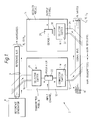
- Figure 1 is a schematic diagram of a first embodiment of the present invention;
- Figure 2 is a schematic diagram of a second embodiment of the present invention in which the receiver modules employ coherent homodyne optical demodulator;
- Figure 3 is a schematic diagram of a third embodiment of the present invention in which the receiver modules employ coherent heterodyne optical demodulators; and
- Figure 4 is a perspective schematic view of an optical bus and a module according to the present invention.
- Referring to Figure 1 an
interconnect network 2 has a reference bus 4 of m optical waveguides Ri to Rm each coupled to a respective optical source of distinct wavelength λi to λm shown collectively as areference generator 8, and asignal bus 10 of N optical waveguides Sl to SN. For clarity there is shown only one transmitter module Ti of upto NxM possible transmitter modules and onereceiver module 14 of up to NxM possible receiver modules connectable to the network of this particular embodiment. - The
transmitter module 12 in this example when fixed in position relative to thebusses 4 and 10 has a first and second group ofwaveguides busses 4 and 10 respectively. Each waveguide of the group ofwaveguides 16 is coupled to one of the waveguides Ri and in turn is optically coupled to areference selector switch 20 which is arranged to couple one of the waveguides Ri to anoptical modulator 22. Themodulator 22 modulates the carrier signal λi coupled from waveguide Si with the information signal to be transmitted. The output of themodulator 22 is couplable via aconnector switch 24 to a selected one waveguide of the group ofwaveguides 18 and hence to a selected one of the waveguides Si. - The
receiver module 14 includes a group ofwaveguides 26 and an N to 1selector switch 28 which in the same manner as theselector switch 16 andwaveguides 16 of thetransmitter module 12 can selectively couple one of the signal waveguides Si to ademodulator 29 via a frequency selectiveoptical filter 30. - An example of a means for coupling the waveguides of the
busses 4 and 10 the module waveguides ofgroups - The principle behind the bus architecture of this embodiment present invention is that the signal bus forms a message bearer bus carrying optical signals from the transmitter modules in a manner that is accessible to the receiver modules and that the reference bus provides a range of optical frequencies of carrier signal which can be selected by a given
transmitter module 12. An interconnection path is established by selecting one wavelength of carrier signal by means of theselector switch 20 modulating the carrier so obtained by the message information and then connecting the modulated carrier via theconnector switch 24 to the selected signal waveguide Si. - Each waveguide Si can therefore carry a wavelength multiplex of M wavelengths, each transmitter being associated with a unique combination of wavelength λi and waveguide Sj.
- A receiver can select the information signal to be received by connecting the appropriate waveguide Sj via the
signal selector switch 28 and passing only the required wavelength λi to the optical demodulator by means of the frequencyselective filter 30. - The principle of using a hierarchy of multiplexing techniques can be extended by, for example, using time coding of transmission, coding of transmissions and so. Thus, for example a three layer hierarchy of space, frequency (as exemplified by the Figure 1 arrangement) together with time domain multiplexing of the information signals to the
modulators 22, each with a dimension of 100 channels would provide an interconnect power of 10⁶. This multiplication of the multiplexing power of each multiplexing technique therefore allows a much greater interconnect power than available from any one technique alone. - The ability to removably couple transmitter and receiver modules onto the
busses 4 and 10 permits ready growth of the network by the additional of modules until all the multiplex combinations are used when whereupon one additional multiplex may be added to the hierarchy to further increase the interconnect power of the network and for transmitter and receiver modules to be unplugged and moved to different locations on the optical bus as necessary. Thus, for example, once NxM transmitters and receivers had been connected to the network, the introduction of P time slot channels would allow expansion of the network to NxMxP transmitters and receivers. - The
transmitter modules waveguides - Alternatively, the transmitter modules may be provided with fixed or tunable optical sources, for example lasers, which eliminates the need for the reference bus 4. If two or more non-spatial hierarchies are employed then the signal bus need have only one waveguide, each transmitter and receiver module being evanescently coupled to it exclusively. In the case of spatial multiplexing, i.e. two or more waveguides in the signal optical bus, the modules can, analogously to the wavelength multiplexing example above, be dedicated or assignable. If the modules are dedicated then the signal connector or signal selector switch may be eliminated, the optical waveguide of the modules being located so that it couples to the required waveguide of the signal optical bus when co-located with the bus.
- Referring now to Figure 2, an
interconnection network 32 is shown which is as thenetwork 2 except that the wavelength selection in thereceiver module 14 is not by way of atunable filter 30 but by means of coherent, homodyne detection. This is achieved by means of anadditional selector switch 34 which selectively couples one of the reference waveguides Ri top thecoherent demodulator 36 corresponding to the wavelength channel to be demultiplexed. - Heterodyne detection can be achieved in a similar manner as by the incorporation of frequency shifters 38 between the reference generator and the
receiver modules 14 of the network of Figure 2 as shown in Figure 3. - A possible structure of the
busses 4, 10, of the groups ofwaveguides flat surface 46 close to the core 44 (as shown on Figure 4 with respect to only one of the figures 44). In this particular embodiment the core was about 0.5µm from the flat surface. - The three D-
fibres polymer substrate 50 30mm. The moulding was performed against a heated optical flat which ensure that the flat surfaces of the D-fibres align accurately in a common plane. Thefibres - The two of the
waveguide substrate 50 coupled to the lasers (not shown) performed the function of the optical bus 4 carrying the power. The third acts as a single signal bus waveguide but was coupled to a laser also to measure the coupling performance. The second substrate, acting as one of the module couplers, was positioned so it overlapped the first by 0.5mm. The close proximity of the cores provided evanescent coupling between them allowing a small fraction of the optical power to be tapped out of the fibre bus into the corresponding waveguide of the second substrate. - A photomicrograph of the
substrate 50 showed that the D-fibres appear as ridges 0.5µm high and 85µm wide, the remainder of the fibre diameter being concealed by polymer 'ears' which grip the fibres and slope away to the general substrate level. The top points of the flat surfaces of the fibre occupy a plane to well within an accuracy of 100nm with a spacing of 250µm ± 20µm. - The power splitting ratios between fibres are displayed in the table below, where the primed numerals indicate the equivalent fibres on the second substrate.

- The cross talk between unwanted pairs of fibres was below the measurement limit of -78dB. The ratio of wanted to unwanted signal was therefore at least 43dB at each tapping point.
- A detailed treatment of the tolerancing of the bus and connector substrates shows that with the present design, a lateral and angular misalignment 250µm, and 1° respectively, a fibre height variation of 0.75µm, or a wavelength change from 1.3 to 1.5µm, each give smaller variation in output power than 3dB. All these parameters are well within achievable engineering limits and have been achieved here. A more critical parameter is the "rocking" of the connector in the two available dimensions. However, by taking advantage of the close tolerance of the planes formed by the D-fibre flats (<100nm), the natural contact of these planes as the connector contacts the bus is well within the tolerance needed. It is obvious that the position of contact along the bus will be immaterial. Many connectors could therefore be connected to the bus along its length.
- Each connector substrate in principle only takes up a few mm of space on the D-fibre bus. The optical loss of D-fibre is below 1dB/m. It can therefore be envisaged that by expanding the present geometries and maintaining the physical tolerances already achieved an optical distribution bus capable of interconnecting large numbers of communicating terminals could be built using present optical technologies.
- Referring now to Figure 5 an optical interconnection network shows a portion an
optical fibre bus 60 having one signal optical D-fibre 62 embedded in athermoplastic substrate 64. A portion of thefibre 62 lies within awall structure 65 having aslot 66 and achannel 68 to avoid contact with the flat of the D-fibre 62. - A
module 70 comprising an optical D-fibre 72 embedded in athermoplastic substrate 74 is dimensioned to be a push fit in thewall structure 68. When pushed intostructure 68 thefibres fibre 72 extends through theslot 66 to a receiver or transmitter as required. - The
module 70 may be provided with a handle to ease removal of themodule 70 from thewall structure 64.
Claims (20)
- An optical interconnection network comprising an optical signal bus (4, 10, 50, 60) having at least one optical waveguide (S, 42, 62) and at least one connector module (70) for connection to the bus, the module having at least one optical waveguide (72) forming an evanescent coupling with a respective waveguide of the signal bus when the module is connected to the bus, characterised in that the signal bus (4, 10, 50, 60) comprises a first substrate (64) supporting a plurality of the optical waveguides (S, 42, 62), the waveguides each having a flat surface substantially co-planar with a surface of the substrate (64); the connector module (70) comprises a second substrate (74) supporting said at least one optical waveguide (72), the waveguide (72) having a flat surface substantially co-planar with a surface of the second substrate (74); and means (65) are provided for releasably coupling the module (70) to the signal bus (10, 50, 60) in a face-to-face relationship to form the said evanescent coupling between the two waveguides.
- A network according to claim 1 in which the releasable coupling means includes upstanding guide walls (65) on one of the substrates (64, 74) adapted to locate respective side edges of the other substrate such that the respective waveguides of the two substrates are aligned relative to one another over the length of the module.
- A network according to claim 2 in which the guide walls (65) include a first pair of opposed walls extending generally parallel to the direction of the waveguides in the respective substrates, and a second pair of opposed walls transverse to the first pair.
- A network according to claim 2 or 3 in which the guide walls (65) include aligned openings (66, 68) forming a passage for the respective optical waveguides in the two substrates when the module is coupled to the bus.
- A network according to any one of the claims 2-4 in which the guide walls define a socket and in which the connector module is a push-fit in the socket.
- A network according to claim 1 in which the releasable coupling is a plug-in coupling.
- A network according to any one of the preceding claims in which the waveguides comprise D-fibres.
- A network according to any one of the preceding claims in which the module (70) has a plurality of waveguides, one positioned to couple to each of the waveguides in the signal bus.
- A network according to claim 8 further comprising:
an optical signal transmitting means (12); and
first transmitter selection means (24) whereby the transmitting means is couplable to a selected one of the signal waveguides. - A network as in claim 9 in which the optical signal transmitting means comprises a tunable laser.
- A network as in claim 8 further comprising a receiving means (14) provided with a first receiver selection means (28) whereby the receiving means is couplable to a selected one of the signal waveguides.
- A network as in claim 11 in which the receiving means (14) comprises a tunable optical filter.
- A network as in claim 9 further comprising a reference optical bus (4) which includes two or more reference optical waveguides each coupled to an optical source (8) of a distinct wavelength, and in which the transmitting means (12) has a waveguide positioned to couple to a predetermined one of the reference waveguides and means (22) for modulating an optical signal coupled from said reference waveguides.
- A network as in claim 13 in which the transmitting means (12) has a plurality of waveguides (16) positioned to couple to each of the reference waveguides, and second transmitter selection means (20) whereby the transmitting means is couplable to a selected one of the reference waveguides.
- A network as in claim 11 further comprising a reference optical bus (14) which includes two or more reference optical waveguides each coupled to an optical source (8) of a distinct wavelength, and in which the receiving means (14) comprises a coherent demodulator (36), and the receiving means has a waveguide positioned to couple to a predetermined one of the reference waveguides whereby the coherent demodulator is couplable to one of the optical sources.
- A network as in claim 15 in which the receiving means (14) has a plurality of waveguides positioned to couple to each of the reference waveguides and a second receiver selection means (34) whereby the receiving means is couplable to a selected one of the reference waveguides.
- A network according to any one of the preceding claims wherein the optical signal bus (4, 10, 50, 60) has plural optical waveguides (S, 42, 62) defining a first plurality of spatially-multiplexed optical signal channels; and the connector module (70) couples an optical signal processor (12, 14) to at least one optical waveguide of the bus, the processor being capable of processing optical signals on at least one of a second plurality of non-spatially multiplexed optical signal channels on said at least one optical waveguide.
- A network according to claim 17 wherein additional signal channels are provided by independently multiplexing the signals transmitted along each of the spatially-multiplexed channels.
- A network according to claim 18 in which the independent multiplexing comprises wavelength and/or time division multiplexing.
- A method of optically interconnecting a transmitter station (12) with a receiver station (14) in an optical communication system having an optical signal bus (4, 10, 50, 60) between the two stations, characterised in that the method comprises forming a plurality of spaced-apart optical waveguides in the signal bus to define a first plurality of spatially-multiplexed optical signal channels releasably coupling a connector module (70) to the signal bus at the transmitter and/or receiver stations to form an evanescent face-to-face coupling between at least one of the waveguides in the bus and respective waveguides in the connector module, and providing a further plurality of non-spatially multiplexed signal channels by independently multiplexing the signals transmitted along each of the spatially-multiplexed channels.
Applications Claiming Priority (2)
| Application Number | Priority Date | Filing Date | Title |
|---|---|---|---|
| GB8902745 | 1989-02-08 | ||
| GB898902745A GB8902745D0 (en) | 1989-02-08 | 1989-02-08 | Optical interconnection network |
Publications (2)
| Publication Number | Publication Date |
|---|---|
| EP0382430A1 EP0382430A1 (en) | 1990-08-16 |
| EP0382430B1 true EP0382430B1 (en) | 1995-09-13 |
Family
ID=10651291
Family Applications (1)
| Application Number | Title | Priority Date | Filing Date |
|---|---|---|---|
| EP90301127A Expired - Lifetime EP0382430B1 (en) | 1989-02-08 | 1990-02-02 | Optical interconnection network |
Country Status (10)
| Country | Link |
|---|---|
| US (2) | US5253094A (en) |
| EP (1) | EP0382430B1 (en) |
| JP (1) | JP3145396B2 (en) |
| AT (1) | ATE127977T1 (en) |
| AU (1) | AU640633B2 (en) |
| CA (1) | CA2048597C (en) |
| DE (1) | DE69022259T2 (en) |
| ES (1) | ES2077638T3 (en) |
| GB (1) | GB8902745D0 (en) |
| WO (1) | WO1990009708A1 (en) |
Families Citing this family (19)
| Publication number | Priority date | Publication date | Assignee | Title |
|---|---|---|---|---|
| JPH05300188A (en) * | 1992-04-23 | 1993-11-12 | Hitachi Ltd | Parallel light transmitting device |
| CN1103930C (en) * | 1994-01-26 | 2003-03-26 | 英国公共电信有限公司 | Optical backplane interconnect |
| JP3006670B2 (en) * | 1995-08-18 | 2000-02-07 | 日本電気株式会社 | Optical submarine branching device and transmission line switching method thereof |
| GB9700008D0 (en) * | 1997-01-02 | 1997-02-19 | Eg & G Inc | Testing transmission lines |
| US6782210B1 (en) * | 1999-08-25 | 2004-08-24 | Nippon Telegraph And Telephone Corporation | Optical packet routing network system based on optical label switching technique |
| GB0000405D0 (en) | 2000-01-11 | 2000-03-01 | British Aerospace | Improvements relating to interfacing embedded optical transmission structures |
| US6937592B1 (en) * | 2000-09-01 | 2005-08-30 | Intel Corporation | Wireless communications system that supports multiple modes of operation |
| US6661949B1 (en) | 2001-03-01 | 2003-12-09 | Kenneth A. James | Totally photonic evanescent switch for optical fibers |
| CN1742512A (en) * | 2002-12-04 | 2006-03-01 | 康宁股份有限公司 | Fast-switching scalable optical interconnection design with fast contention resolution |
| US20050259919A1 (en) * | 2003-12-22 | 2005-11-24 | Aldridge Nigel B | Optical connector arrangement |
| US7366368B2 (en) * | 2004-06-15 | 2008-04-29 | Intel Corporation | Optical add/drop interconnect bus for multiprocessor architecture |
| US9417418B2 (en) | 2011-09-12 | 2016-08-16 | Commscope Technologies Llc | Flexible lensed optical interconnect device for signal distribution |
| US9488788B2 (en) | 2012-09-28 | 2016-11-08 | Commscope Technologies Llc | Fiber optic cassette |
| US9223094B2 (en) | 2012-10-05 | 2015-12-29 | Tyco Electronics Nederland Bv | Flexible optical circuit, cassettes, and methods |
| WO2018046677A1 (en) | 2016-09-08 | 2018-03-15 | CommScope Connectivity Belgium BVBA | Telecommunications distribution elements |
| MX2020002878A (en) | 2017-10-02 | 2020-07-22 | Commscope Technologies Llc | Fiber optic circuit and preparation method. |
| US10895687B2 (en) | 2018-10-31 | 2021-01-19 | Corning Research & Development Corporation | Alignment ferrule assemblies and connectors for evanescent optical couplers and evanescent optical couplers using same |
| US12339511B2 (en) | 2020-03-31 | 2025-06-24 | Commscope Technologies Llc | Fiber optic cable management systems and methods |
| EP4178132B1 (en) * | 2021-11-03 | 2024-01-10 | Deutsche Telekom AG | Method for establishing or switching an optical transmission path in order to transmit an optical signal, optical network node for establishing or switching an optical transmission path in order to transmit an optical signal, backbone network, aggregation network or telecommunications network, system, program and computer-readable medium |
Family Cites Families (22)
| Publication number | Priority date | Publication date | Assignee | Title |
|---|---|---|---|---|
| US3986020A (en) * | 1975-09-25 | 1976-10-12 | Bell Telephone Laboratories, Incorporated | Common medium optical multichannel exchange and switching system |
| US4234970A (en) * | 1977-11-03 | 1980-11-18 | Elliott Brothers (London) Limited | Fiber optic communication system |
| US4451916A (en) * | 1980-05-12 | 1984-05-29 | Harris Corporation | Repeatered, multi-channel fiber optic communication network having fault isolation system |
| DE3218022C2 (en) * | 1981-05-13 | 1984-08-02 | Felten & Guilleaume Fernmeldeanlagen GmbH, 8500 Nürnberg | Optical device for multiplexing |
| US4444460A (en) * | 1981-05-26 | 1984-04-24 | Gould Inc. | Optical fiber apparatus including subtstrate ruggedized optical fibers |
| FR2526255A1 (en) * | 1982-04-30 | 1983-11-04 | Rozenwaig Boris | OPTO-ELECTRONIC SWITCHES WITH MULTI-CHANNEL SELECTOR DEVICES FOR BROADBAND TELECOMMUNICATIONS SYSTEMS AND OPTO-ELECTRONIC SELECTOR DEVICES FOR SAID SWITCHES |
| US4611884A (en) * | 1982-11-24 | 1986-09-16 | Magnetic Controls Company | Bi-directional optical fiber coupler |
| US4592043A (en) * | 1983-07-08 | 1986-05-27 | At&T Bell Laboratories | Wavelength division multiplexing optical communications systems |
| WO1985000484A1 (en) * | 1983-07-08 | 1985-01-31 | American Telephone & Telegraph Company | Wavelength division multiplexing optical communications systems |
| US4699449A (en) * | 1985-03-05 | 1987-10-13 | Canadian Patents And Development Limited-Societe Canadienne Des Brevets Et D'exploitation Limitee | Optoelectronic assembly and method of making the same |
| GB2182516A (en) * | 1985-11-01 | 1987-05-13 | Stc Plc | Optical fibre network |
| EP0223258B1 (en) * | 1985-11-22 | 1994-01-26 | Nec Corporation | Wavelength division optical switching system having wavelength switching light modulators |
| US4742576A (en) * | 1985-12-23 | 1988-05-03 | Polaroid Corporation | Optical communication system employing coherent detection and method |
| US4759011A (en) * | 1986-03-03 | 1988-07-19 | Polaroid Corporation | Intranetwork and internetwork optical communications system and method |
| US4701909A (en) * | 1986-07-24 | 1987-10-20 | American Telephone And Telegraph Company, At&T Bell Laboratories | Collision detection technique for an optical passive star local area network using CSMA/CD |
| CA1331800C (en) * | 1987-09-30 | 1994-08-30 | Syuji Suzuki | Time and wavelength division switching system |
| US4883743A (en) * | 1988-01-15 | 1989-11-28 | E. I. Du Pont De Nemours And Company | Optical fiber connector assemblies and methods of making the assemblies |
| US4846540A (en) * | 1988-01-25 | 1989-07-11 | Bell Communications Research, Inc. | Optical wavegide junction |
| US4873681A (en) * | 1988-01-26 | 1989-10-10 | Bell Communications Research, Inc. | Hybrid optical and electronic packet switch |
| EP0335104A3 (en) * | 1988-03-31 | 1991-11-06 | Siemens Aktiengesellschaft | Arrangement to optically couple one or a plurality of optical senders to one or a plurality of optical receivers of one or a plurality of integrated circuits |
| GB8902746D0 (en) * | 1989-02-08 | 1989-03-30 | British Telecomm | Communications network |
| JP5857724B2 (en) | 2011-12-20 | 2016-02-10 | コニカミノルタ株式会社 | ORGANIC ELECTROLUMINESCENT ELEMENT MATERIAL, ORGANIC ELECTROLUMINESCENT ELEMENT, DISPLAY DEVICE, LIGHTING DEVICE, AND ORGANIC ELECTROLUMINESCENT ELEMENT MANUFACTURING METHOD |
-
1989
- 1989-02-08 GB GB898902745A patent/GB8902745D0/en active Pending
-
1990
- 1990-02-02 DE DE69022259T patent/DE69022259T2/en not_active Expired - Lifetime
- 1990-02-02 EP EP90301127A patent/EP0382430B1/en not_active Expired - Lifetime
- 1990-02-02 ES ES90301127T patent/ES2077638T3/en not_active Expired - Lifetime
- 1990-02-02 AT AT90301127T patent/ATE127977T1/en active
- 1990-02-05 US US07/762,025 patent/US5253094A/en not_active Expired - Lifetime
- 1990-02-05 WO PCT/GB1990/000169 patent/WO1990009708A1/en not_active Ceased
- 1990-02-05 JP JP50318490A patent/JP3145396B2/en not_active Expired - Lifetime
- 1990-02-05 CA CA002048597A patent/CA2048597C/en not_active Expired - Fee Related
- 1990-02-05 AU AU50926/90A patent/AU640633B2/en not_active Ceased
-
1993
- 1993-03-26 US US08/037,581 patent/US5504607A/en not_active Expired - Lifetime
Also Published As
| Publication number | Publication date |
|---|---|
| ATE127977T1 (en) | 1995-09-15 |
| JP3145396B2 (en) | 2001-03-12 |
| DE69022259T2 (en) | 1996-07-25 |
| JPH04503445A (en) | 1992-06-18 |
| AU640633B2 (en) | 1993-09-02 |
| WO1990009708A1 (en) | 1990-08-23 |
| US5504607A (en) | 1996-04-02 |
| AU5092690A (en) | 1990-09-05 |
| US5253094A (en) | 1993-10-12 |
| EP0382430A1 (en) | 1990-08-16 |
| DE69022259D1 (en) | 1995-10-19 |
| ES2077638T3 (en) | 1995-12-01 |
| CA2048597A1 (en) | 1990-08-09 |
| CA2048597C (en) | 1999-02-02 |
| GB8902745D0 (en) | 1989-03-30 |
Similar Documents
| Publication | Publication Date | Title |
|---|---|---|
| US5253094A (en) | Optical interconnection network | |
| US6661940B2 (en) | Apparatus and method for rebroadcasting signals in an optical backplane bus system | |
| CA2181336C (en) | Optical backplane interconnect | |
| US20020102046A1 (en) | Opto-electronic distributed crossbar switch | |
| GB2334396A (en) | Connecting circuit boards using optical WDM signals | |
| CA2477757A1 (en) | Apparatus and method for using fiber optic arrays in optical communication systems | |
| EP0856755A1 (en) | Optical waveguide coupler having low insertion loss | |
| US4957339A (en) | Optical communication system, particularly in the subscriber area | |
| EP0208729A1 (en) | OPTICAL NETWORK. | |
| EP0518570B1 (en) | Optical wavelength-division multiplex modules | |
| CN217279012U (en) | 1X 5 optical splitter chip | |
| EP1060581B1 (en) | Testing of optical transmitter and receiver modules | |
| US5091985A (en) | Optical signal connection device for units to be inserted in a rack | |
| CN104503039A (en) | Direct-dimming-type InP-based monolithic integration few-mode optical communication transmitter chip | |
| EP1188085A1 (en) | An optical transmitter-receiver module | |
| MacKenzie et al. | Optical interconnect based on a fibre bus | |
| CN224216905U (en) | Integrated wave combining and dividing device | |
| CN220962024U (en) | Optical module, optical system, optical transceiver module, laser radar and optical amplification system | |
| EP0530915A1 (en) | Telecommunication network comprising a single glass fibre cable | |
| JPS5915422B2 (en) | Optical transmission method between packages | |
| US20040114870A1 (en) | Optical add/drop patch cord | |
| SUMIDA et al. | High-silica guided-wave hybrid optical transmitting-receiving module | |
| MacKenzie et al. | D-fiber optical backplane interconnect | |
| CN121603107A (en) | Single-fiber bidirectional coherent optical module, optical communication equipment and network | |
| Smith et al. | Multidimensional optical switching networks |
Legal Events
| Date | Code | Title | Description |
|---|---|---|---|
| PUAI | Public reference made under article 153(3) epc to a published international application that has entered the european phase |
Free format text: ORIGINAL CODE: 0009012 |
|
| AK | Designated contracting states |
Kind code of ref document: A1 Designated state(s): AT BE CH DE DK ES FR GB GR IT LI LU NL SE |
|
| 17P | Request for examination filed |
Effective date: 19910110 |
|
| 17Q | First examination report despatched |
Effective date: 19940204 |
|
| GRAA | (expected) grant |
Free format text: ORIGINAL CODE: 0009210 |
|
| AK | Designated contracting states |
Kind code of ref document: B1 Designated state(s): AT BE CH DE DK ES FR GB GR IT LI LU NL SE |
|
| PG25 | Lapsed in a contracting state [announced via postgrant information from national office to epo] |
Ref country code: BE Effective date: 19950913 Ref country code: AT Effective date: 19950913 Ref country code: DK Effective date: 19950913 Ref country code: GR Free format text: LAPSE BECAUSE OF FAILURE TO SUBMIT A TRANSLATION OF THE DESCRIPTION OR TO PAY THE FEE WITHIN THE PRESCRIBED TIME-LIMIT Effective date: 19950913 |
|
| REF | Corresponds to: |
Ref document number: 127977 Country of ref document: AT Date of ref document: 19950915 Kind code of ref document: T |
|
| ITF | It: translation for a ep patent filed | ||
| REF | Corresponds to: |
Ref document number: 69022259 Country of ref document: DE Date of ref document: 19951019 |
|
| REG | Reference to a national code |
Ref country code: ES Ref legal event code: FG2A Ref document number: 2077638 Country of ref document: ES Kind code of ref document: T3 |
|
| ET | Fr: translation filed | ||
| PG25 | Lapsed in a contracting state [announced via postgrant information from national office to epo] |
Ref country code: LU Free format text: LAPSE BECAUSE OF NON-PAYMENT OF DUE FEES Effective date: 19960229 |
|
| PLBE | No opposition filed within time limit |
Free format text: ORIGINAL CODE: 0009261 |
|
| STAA | Information on the status of an ep patent application or granted ep patent |
Free format text: STATUS: NO OPPOSITION FILED WITHIN TIME LIMIT |
|
| 26N | No opposition filed | ||
| REG | Reference to a national code |
Ref country code: GB Ref legal event code: 732E |
|
| REG | Reference to a national code |
Ref country code: GB Ref legal event code: IF02 |
|
| PGFP | Annual fee paid to national office [announced via postgrant information from national office to epo] |
Ref country code: CH Payment date: 20020118 Year of fee payment: 13 |
|
| PGFP | Annual fee paid to national office [announced via postgrant information from national office to epo] |
Ref country code: NL Payment date: 20020121 Year of fee payment: 13 |
|
| PGFP | Annual fee paid to national office [announced via postgrant information from national office to epo] |
Ref country code: SE Payment date: 20020122 Year of fee payment: 13 |
|
| PGFP | Annual fee paid to national office [announced via postgrant information from national office to epo] |
Ref country code: ES Payment date: 20020205 Year of fee payment: 13 |
|
| PG25 | Lapsed in a contracting state [announced via postgrant information from national office to epo] |
Ref country code: SE Free format text: LAPSE BECAUSE OF NON-PAYMENT OF DUE FEES Effective date: 20030203 Ref country code: ES Free format text: LAPSE BECAUSE OF NON-PAYMENT OF DUE FEES Effective date: 20030203 |
|
| PG25 | Lapsed in a contracting state [announced via postgrant information from national office to epo] |
Ref country code: CH Free format text: LAPSE BECAUSE OF NON-PAYMENT OF DUE FEES Effective date: 20030228 Ref country code: LI Free format text: LAPSE BECAUSE OF NON-PAYMENT OF DUE FEES Effective date: 20030228 |
|
| PG25 | Lapsed in a contracting state [announced via postgrant information from national office to epo] |
Ref country code: NL Free format text: LAPSE BECAUSE OF NON-PAYMENT OF DUE FEES Effective date: 20030901 |
|
| EUG | Se: european patent has lapsed | ||
| REG | Reference to a national code |
Ref country code: CH Ref legal event code: PL |
|
| NLV4 | Nl: lapsed or anulled due to non-payment of the annual fee |
Effective date: 20030901 |
|
| REG | Reference to a national code |
Ref country code: ES Ref legal event code: FD2A Effective date: 20030203 |
|
| PG25 | Lapsed in a contracting state [announced via postgrant information from national office to epo] |
Ref country code: IT Free format text: LAPSE BECAUSE OF NON-PAYMENT OF DUE FEES;WARNING: LAPSES OF ITALIAN PATENTS WITH EFFECTIVE DATE BEFORE 2007 MAY HAVE OCCURRED AT ANY TIME BEFORE 2007. THE CORRECT EFFECTIVE DATE MAY BE DIFFERENT FROM THE ONE RECORDED. Effective date: 20050202 |
|
| REG | Reference to a national code |
Ref country code: GB Ref legal event code: 732E |
|
| REG | Reference to a national code |
Ref country code: FR Ref legal event code: TP |
|
| PGFP | Annual fee paid to national office [announced via postgrant information from national office to epo] |
Ref country code: DE Payment date: 20090219 Year of fee payment: 20 |
|
| PGFP | Annual fee paid to national office [announced via postgrant information from national office to epo] |
Ref country code: GB Payment date: 20090219 Year of fee payment: 20 |
|
| PGFP | Annual fee paid to national office [announced via postgrant information from national office to epo] |
Ref country code: FR Payment date: 20090220 Year of fee payment: 20 |
|
| REG | Reference to a national code |
Ref country code: GB Ref legal event code: PE20 Expiry date: 20100201 |
|
| PG25 | Lapsed in a contracting state [announced via postgrant information from national office to epo] |
Ref country code: GB Free format text: LAPSE BECAUSE OF EXPIRATION OF PROTECTION Effective date: 20100201 |
|
| PG25 | Lapsed in a contracting state [announced via postgrant information from national office to epo] |
Ref country code: DE Free format text: LAPSE BECAUSE OF EXPIRATION OF PROTECTION Effective date: 20100202 |