EP0381735B1 - Design and fabrication of synthetic superconductors - Google Patents
Design and fabrication of synthetic superconductors Download PDFInfo
- Publication number
- EP0381735B1 EP0381735B1 EP89908662A EP89908662A EP0381735B1 EP 0381735 B1 EP0381735 B1 EP 0381735B1 EP 89908662 A EP89908662 A EP 89908662A EP 89908662 A EP89908662 A EP 89908662A EP 0381735 B1 EP0381735 B1 EP 0381735B1
- Authority
- EP
- European Patent Office
- Prior art keywords
- layers
- layer
- thickness
- conducting
- lower conducting
- Prior art date
- Legal status (The legal status is an assumption and is not a legal conclusion. Google has not performed a legal analysis and makes no representation as to the accuracy of the status listed.)
- Expired - Lifetime
Links
- 239000002887 superconductor Substances 0.000 title claims abstract description 32
- 238000004519 manufacturing process Methods 0.000 title description 10
- 239000002800 charge carrier Substances 0.000 claims abstract description 26
- 230000008021 deposition Effects 0.000 claims abstract description 10
- 238000007747 plating Methods 0.000 claims abstract description 6
- 239000000463 material Substances 0.000 claims description 25
- 239000000969 carrier Substances 0.000 claims description 19
- 238000000034 method Methods 0.000 claims description 14
- 239000004065 semiconductor Substances 0.000 claims description 13
- 238000000151 deposition Methods 0.000 claims description 11
- 239000002245 particle Substances 0.000 claims description 9
- 229910052751 metal Inorganic materials 0.000 claims description 6
- 239000002184 metal Substances 0.000 claims description 6
- JBRZTFJDHDCESZ-UHFFFAOYSA-N AsGa Chemical group [As]#[Ga] JBRZTFJDHDCESZ-UHFFFAOYSA-N 0.000 claims description 5
- 229910001218 Gallium arsenide Inorganic materials 0.000 claims description 5
- RYGMFSIKBFXOCR-UHFFFAOYSA-N Copper Chemical compound [Cu] RYGMFSIKBFXOCR-UHFFFAOYSA-N 0.000 claims description 4
- 229910052802 copper Inorganic materials 0.000 claims description 4
- 239000010949 copper Substances 0.000 claims description 4
- 239000011810 insulating material Substances 0.000 claims description 4
- 239000007769 metal material Substances 0.000 claims description 4
- RTAQQCXQSZGOHL-UHFFFAOYSA-N Titanium Chemical compound [Ti] RTAQQCXQSZGOHL-UHFFFAOYSA-N 0.000 claims description 3
- 229910052782 aluminium Inorganic materials 0.000 claims description 3
- XAGFODPZIPBFFR-UHFFFAOYSA-N aluminium Chemical compound [Al] XAGFODPZIPBFFR-UHFFFAOYSA-N 0.000 claims description 3
- 230000015572 biosynthetic process Effects 0.000 claims description 3
- 238000009826 distribution Methods 0.000 claims description 3
- 238000004544 sputter deposition Methods 0.000 claims description 3
- 239000010936 titanium Substances 0.000 claims description 3
- 229910052719 titanium Inorganic materials 0.000 claims description 3
- OKTJSMMVPCPJKN-UHFFFAOYSA-N Carbon Chemical compound [C] OKTJSMMVPCPJKN-UHFFFAOYSA-N 0.000 claims description 2
- 229910052799 carbon Inorganic materials 0.000 claims description 2
- 150000002222 fluorine compounds Chemical class 0.000 claims description 2
- 239000011521 glass Substances 0.000 claims description 2
- PCHJSUWPFVWCPO-UHFFFAOYSA-N gold Chemical compound [Au] PCHJSUWPFVWCPO-UHFFFAOYSA-N 0.000 claims description 2
- 229910052737 gold Inorganic materials 0.000 claims description 2
- 239000010931 gold Substances 0.000 claims description 2
- 229910052709 silver Inorganic materials 0.000 claims description 2
- 239000004332 silver Substances 0.000 claims description 2
- 239000004411 aluminium Substances 0.000 claims 2
- BQCADISMDOOEFD-UHFFFAOYSA-N Silver Chemical compound [Ag] BQCADISMDOOEFD-UHFFFAOYSA-N 0.000 claims 1
- 229910052790 beryllium Inorganic materials 0.000 claims 1
- ATBAMAFKBVZNFJ-UHFFFAOYSA-N beryllium atom Chemical compound [Be] ATBAMAFKBVZNFJ-UHFFFAOYSA-N 0.000 claims 1
- 229910003460 diamond Inorganic materials 0.000 claims 1
- 239000010432 diamond Substances 0.000 claims 1
- 150000004767 nitrides Chemical class 0.000 claims 1
- 230000003993 interaction Effects 0.000 abstract description 2
- 239000013078 crystal Substances 0.000 description 11
- 238000010586 diagram Methods 0.000 description 7
- 238000000926 separation method Methods 0.000 description 7
- QPLDLSVMHZLSFG-UHFFFAOYSA-N Copper oxide Chemical compound [Cu]=O QPLDLSVMHZLSFG-UHFFFAOYSA-N 0.000 description 6
- 239000005751 Copper oxide Substances 0.000 description 6
- 125000004429 atom Chemical group 0.000 description 6
- 229910000431 copper oxide Inorganic materials 0.000 description 6
- 230000000694 effects Effects 0.000 description 5
- 239000012212 insulator Substances 0.000 description 5
- OYPRJOBELJOOCE-UHFFFAOYSA-N Calcium Chemical compound [Ca] OYPRJOBELJOOCE-UHFFFAOYSA-N 0.000 description 3
- 229910052788 barium Inorganic materials 0.000 description 3
- DSAJWYNOEDNPEQ-UHFFFAOYSA-N barium atom Chemical compound [Ba] DSAJWYNOEDNPEQ-UHFFFAOYSA-N 0.000 description 3
- 229910052791 calcium Inorganic materials 0.000 description 3
- 239000011575 calcium Substances 0.000 description 3
- 239000004020 conductor Substances 0.000 description 3
- 239000003989 dielectric material Substances 0.000 description 3
- 239000000203 mixture Substances 0.000 description 3
- 238000005381 potential energy Methods 0.000 description 3
- 239000000758 substrate Substances 0.000 description 3
- 229910052716 thallium Inorganic materials 0.000 description 3
- BKVIYDNLLOSFOA-UHFFFAOYSA-N thallium Chemical compound [Tl] BKVIYDNLLOSFOA-UHFFFAOYSA-N 0.000 description 3
- VYPSYNLAJGMNEJ-UHFFFAOYSA-N Silicium dioxide Chemical compound O=[Si]=O VYPSYNLAJGMNEJ-UHFFFAOYSA-N 0.000 description 2
- 150000001875 compounds Chemical class 0.000 description 2
- 230000005686 electrostatic field Effects 0.000 description 2
- 238000009472 formulation Methods 0.000 description 2
- 229910052727 yttrium Inorganic materials 0.000 description 2
- VWQVUPCCIRVNHF-UHFFFAOYSA-N yttrium atom Chemical compound [Y] VWQVUPCCIRVNHF-UHFFFAOYSA-N 0.000 description 2
- 229910052581 Si3N4 Inorganic materials 0.000 description 1
- 238000002441 X-ray diffraction Methods 0.000 description 1
- 239000000654 additive Substances 0.000 description 1
- 230000000996 additive effect Effects 0.000 description 1
- 239000000919 ceramic Substances 0.000 description 1
- 238000005229 chemical vapour deposition Methods 0.000 description 1
- 239000000470 constituent Substances 0.000 description 1
- 238000010276 construction Methods 0.000 description 1
- 238000001514 detection method Methods 0.000 description 1
- 230000005684 electric field Effects 0.000 description 1
- 230000009881 electrostatic interaction Effects 0.000 description 1
- 238000005290 field theory Methods 0.000 description 1
- 239000003574 free electron Substances 0.000 description 1
- 238000010191 image analysis Methods 0.000 description 1
- 239000007788 liquid Substances 0.000 description 1
- 238000002488 metal-organic chemical vapour deposition Methods 0.000 description 1
- 150000002739 metals Chemical class 0.000 description 1
- 238000001451 molecular beam epitaxy Methods 0.000 description 1
- 125000002524 organometallic group Chemical group 0.000 description 1
- 125000004430 oxygen atom Chemical group O* 0.000 description 1
- 235000012239 silicon dioxide Nutrition 0.000 description 1
- 239000000377 silicon dioxide Substances 0.000 description 1
- HQVNEWCFYHHQES-UHFFFAOYSA-N silicon nitride Chemical compound N12[Si]34N5[Si]62N3[Si]51N64 HQVNEWCFYHHQES-UHFFFAOYSA-N 0.000 description 1
- 239000000126 substance Substances 0.000 description 1
- 230000002194 synthesizing effect Effects 0.000 description 1
Images


Classifications
-
- H—ELECTRICITY
- H10—SEMICONDUCTOR DEVICES; ELECTRIC SOLID-STATE DEVICES NOT OTHERWISE PROVIDED FOR
- H10N—ELECTRIC SOLID-STATE DEVICES NOT OTHERWISE PROVIDED FOR
- H10N60/00—Superconducting devices
- H10N60/80—Constructional details
- H10N60/85—Superconducting active materials
- H10N60/855—Ceramic superconductors
- H10N60/857—Ceramic superconductors comprising copper oxide
Definitions
- the present invention relates to a synthetic superconductor operating at temperatures substantially above those temperatures near absolute zero where conventional superconduction has been observed. These elevated superconduction temperatures are already seen in a selected group of chemical compounds in the vicinity of 100°K, for example.
- Such high temperature superconductors comprise a crystal structure containing a copper oxide formulation in which various elements, including thallium, calcium, yttrium and barium, to name a few, are incorporated.
- the particular collection of elements leading to compounds which exhibit good superconductivity properties are obtained through trial and error.
- Various theories have attempted to provide a description of superconductivity. They all attribute such superconductivity to layers of two dimensional copper and oxygen atoms within the crystal lattice. These layers are separated by low conductivity monodirectional filaments or one dimensional chains of copper oxide in the crystal structure.
- the present invention consists in a heterogeneous multilayer superconductor comprising a plurality of higher conducting layers formed of a metallic material or doped semiconductor material, having a first electrical conductance in a direction parallel to the layer and a first charge carrier density per unit area of the layer; at least one lower conducting layer formed of a metallic material or doped semiconductor material, having a second said electrical conductance lower than the first and a second said charge carrier density per unit area lower than said first charge carrier density; and a plurality of electrically insulating layers wherein each of said higher conducting layers is separated from a lower conducting layer by one of said electrically insulating layers, the higher and lower conducting layers being from one to several atoms in thickness and the electrically insulating layers having a thickness of several ⁇ ngströms whereby said higher and lower conducting layers cooperate to cause charge carriers in the first higher conducting layers to be electrostatically bound by a potential well induced by a charge distribution in the lower conducting layer, to provide superconduction in a direction parallel to said layers.
- the spacing function is provided by any insulating material including dielectrics, free space, etc.
- the layers, their spacing and conductivity levels are selected to produce electrostatic forces between the free charge carriers of the higher and lower conducting layers which cause the carriers in the lower conducting layers to be electrostatically paired or grouped in small clusters defined by potential wells resulting from the properties and geometry of the layered structure.
- the resulting construction provides for superconductivity through the interplay of the higher and lower conducting layers.
- the lower conducting layer is thus central to the exhibited superconductivity.
- the superconductors according to the present invention are fabricated, in one embodiment, by depositing or plating layers of the higher and lower conducting strata one to several atoms in thickness, separated by an insulator, typically of very low dielectric constant, in order to permit the electrostatic forces required for charge pairing in the lower conducting layers to be strong.
- the arrangement of the present invention is distinct from conventional elevated temperature superconducting materials which comprise a crystal of, among other constituents, copper oxide as illustrated in Figs. 1A-1C.
- crystal structures of the indicated formulation have been analyzed by X-ray diffraction to indicate a plurality of generally parallel planes 12 of copper oxide 14. These are spaced by one dimensional linear chains 16 of copper oxide 18.
- Additive atoms of thallium, barium, calcium, etc. are interspaced in the crystal to promote free carrier formation. The superconduction is envisioned as occurring the planes 12. Fabrication of the crystal structure of Figs.
- 1A-1C includes combining the requisite elements, such as selected combinations of thallium, yttrium, barium or calcium, with copper and their oxides, for example.
- the controls over fabrication of superconducting materials according to this recipe is not understood and obtaining superconducting results is strictly by trial and error.
- the crystal structure which results when the lattice is realized is a complex combination of various elements and copper oxide networks without any predictability of results based upon the crystal structure appearance.
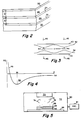
- a superconductor according to the present invention comprises a set of higher conducting layers 20 and 22 separated by a lower conducting layer 24 with each of the higher or lower conducting layers 20, 22 and 24 spaced by insulating layers 26 and 28 which may be a dielectric material or free space.
- the layered structure is typically assembled on a substrate 30 by plating or particle deposition and may be repeated a plurality of times upon top of the layer 20.
- the layers 20 and 22 will be the same metal conductor while the layers 26 and 28 will be the same insulating or dielectric material.
- Various processes may be used to produce each layer.
- particle deposition by sputtering and other techniques can be used to produce a disordered amorphous or polycrystalline film layer.
- Single crystal expitaxial film layers can be grown by chemical vapor deposition (CVD or MOCVD) organo metallic CVD, or high vacuum molecular beam epitaxy (MBE).
- CVD or MOCVD chemical vapor deposition
- MBE high vacuum molecular beam epitaxy
- Assisted or reactive deposition, liquid melt deposition as well as plating may be used as appropriate.
- the layer 24 in one embodiment is achieved by depositing the same material utilized to produce the layers 20 and 22 but at a sufficiently lower thickness in order to lower its overall conductivity according to the theoretical considerations presented below.
- the layer 24 may be of a thickness, for example, of three atoms while the layers 20 and 30 may be several times that in thickness.
- the materials for the layers 20 and 22, and optionally layer 24, are typically chosen to have good electrical conductivity properties and in particular are selected for as many free electrons per atom as can be conveniently obtained. Typical examples of such materials are metal like, gold, silver, berryllium and copper.
- the partial or lesser conducting layer 24, if of a different material than the metals used for the layers 20 and 22, may be of titanium, or aluminum as examples. None of these examples are intended to be limitations on the metal or its nature for the layers 20, 22 and 24. The theoretical considerations presented below will indicate the guidelines for the use of other materials.
- the layers 20 and 24 as well as 22 and 24 are spaced by a thickness, "C", which is typically on the order of ten Angstroms, but is more generally governed by the theoretical considerations identified below. It is preferable that the dielectric constant of the layers 26 and 28 separating the layers 20, 24 and 22 be relatively low, typically as close to 1 as is reasonable. This is for practical considerations of dimensioning the layers and not seen as a limitation.
- Typical examples for the layers 26 and 28 include silicon dioxide, silicon nitride, various fluoride compounds, glasses, and a diamond-like carbon film layer.
- the lower conducting layer of a doped GaAs semiconductor and the higher conducting layer of a grown metal layer or degeneratively doped GaAs are convenient to make the lower conducting layer of a doped GaAs semiconductor and the higher conducting layer of a grown metal layer or degeneratively doped GaAs.
- the conductive layers would be separated by grown layers of insulator, Al X Ga 1-x As.
- the higher conducting layer can have the number of charge carriers in a one cm square area of thickness t equal to or greater than 10 13 . This implies a thickness t, for this layer greater than 10 13 /n, where n is the density of charge carriers per cm 3 .
- the number of charge carriers in a one cm square area of thickness t should be less than 10 12 .
- the layer thickness T is then constrained to be less than 10 12 /n. If a one atom thick layer is considered, then n is limited to be less than 3 X 10 19 /cm 3 for the lower conducting layer. For the higher conducting layer n could exceed 10 21 /cm 3 .
- first and second conducting plates 40 and 42 are shown to represent respectively the conductors 20 and 22. Centered between the plates 40 and 42 are charge carriers 44 which may be either positive or negative charge carriers typically representing the free or partially free charge carriers in the lower conducting layer 24.
- charge carriers 44 may be either positive or negative charge carriers typically representing the free or partially free charge carriers in the lower conducting layer 24.
- image analysis in which case an array of additional alternately charged particles 46 are substituted for the plates 40 and 42.
- the resulting field and potential equation results from the superposition of the contributions from each carrier 44 and each particle 46.
- the resulting field can be summarized in a potential energy diagram illustrated in Fig. 4 as a function of the distance, "d", separating the charge carriers 44 from each other.
- Different sets of potential curves 48 can be generated for different values of "C".
- C the distance
- a potential diagram as illustrated in Fig. 4 will result.
- the potential curve shows a potential well 50 indicating that the carriers 44, contrary to conventional thinking, will not be repulsed from each other but will rather be attracted to each other to a stable separation distance, represented by the bottom of the potential well 50, at the separation "d o ".
- each of the carriers 44 will cause free carriers in the layers 40 and 42 to move under the influence of the electrostatic effects produced by the carriers 44 creating charge distributions 52 and 54 respectively in each plate as illustrated.
- the charges in the plates 40 and 42 will cause an attractive effect between the carriers 44. Because of the conductivity of the plates 40 and 42 the charge bunching in plates 40 and 42 produced by one carrier 44 will have no net effect on that carrier 44 but the charge bunching produced by its neighboring carrier 44 will indeed be felt by the first carrier 44 in such manner as to draw the carriers 44 together forming pairs despite being of the same charge.
- the layer 24, containing the carriers 44 should have relatively fewer free or partially free charge carriers in order that their electric fields will not be shielded and cancelled, so that effective pairing or grouping in repeating clusters of carriers 44 will occur according to the electrostatics described above. If the charge carriers in the layer 24 are too prevalent, there will result a situation simply reflected by two parallel conductors.
- the dimension of the separation of the conducting layers, "C” is governed by the consideration that the binding energy between the charge carriers 44, considered as the difference between the bottom of the energy well 50 and the asymptotically approached limit of potential energy 54, reached at "d" equal to infinity, varies as a function of a factor representing the conductivity of the layers 20 and 22 over the product of the separation, "C/2" and the dielectric constant of the insulators 26 and 28.
- hindsight indicates that fitting this theoretical potential energy theory to the experimentally observed results for known materials of the type illustrated in Fig. 1 indicates a substantially perfect fit, confirming the accuracy of the theory in predicting superconductivity.
- a more practical approach to achieving superconductivity is achieved by synthesizing materials constituted of layers of the sort illustrated in Fig. 2 or a more controlled approach in which strata of conducting and lesser conducting layers are achieved.
- the constraints on the dimensions are indeed limited only by the necessity to achieve a potential well effect as illustrated in Fig. 4 and a controlled number of charge carriers, holes or electrons, freely available in the layer 24, as well as a limited number of carriers paired or grouped in each potential well, typically a few electrons or holes as the case may be.
- the diameter of the grouped carrier ensemble is typically on the same size order, 10 to 15 Angstroms, as the separation, "C", of the conducting layers 20 and 22.
- the important considerations are thus a relatively good level or density of free charge carriers in the conducting layers 20 and 22 and a more restricted availability in the layers 24.
- a separation of the layers as a function of the dielectric constant is also important. Consistent with the above observations the conducting layers 20 and 22 will typically have the number of carriers in a one cm 2 area be greater than 10 13 . For practical thicknesses, the volume density of carriers will be greater than 10 21 per cm 3 .
- the layers should be of high purity as well.
- the lower conducting layers will have volume densities of carriers on the order of 10 12 particles per cm 3 or less and a Debye length which is greater than the average interparticle spacing in order to permit the electrostatic fields to act through the lower conducting layers.
- Apparatus for producing the layered structure of the embodiment represented in Fig. 2 can include any form of appropriate deposition, plating or microstructure forming apparatus. Such apparatus is illustrated in Fig. 5 in general in which layers 62, 64, 66 on a substrate 68 are deposited, grown or otherwise built up by any of the processes noted above or any other suitable processes within a vacuum chamber 60.
- An evacuating apparatus 61 maintains the interior 72 of the chamber 60 at a low enough pressure which prevents interference with the layer generation process. Particles 74 from a source 70, collect on the top surface of the layered structure.
- step 80 the substrate 66 is placed into the chamber 60 and an appropriate vacuum, achieved. With the appropriate vacuum, a subsequent step 82 deposits the first layer 22. Subsequent steps 84, 86, 88, and 90 deposit the layers 28, 24, 26, and 20 as illustrated above. Steps 84 through 90 may be repeated by exiting a decision step 92 on a branch 94 calling for repetition of the layers in a repeating sandwich structure. Alternatively, decision step 92 may limit or terminate the layering according to programmed control produced by a controller 96. The commencement of layer formation may begin at any layer so long as the correct sequence is followed.
- Additional instrumentation may be associated with the processing chamber 60, such as thickness detection instrumentation, in order to automatically terminate deposition as a function of deposited layer thickness.
Landscapes
- Chemical & Material Sciences (AREA)
- Engineering & Computer Science (AREA)
- Ceramic Engineering (AREA)
- Superconductor Devices And Manufacturing Methods Thereof (AREA)
- Superconductors And Manufacturing Methods Therefor (AREA)
- Containers, Films, And Cooling For Superconductive Devices (AREA)
Abstract
Description
- The present invention relates to a synthetic superconductor operating at temperatures substantially above those temperatures near absolute zero where conventional superconduction has been observed. These elevated superconduction temperatures are already seen in a selected group of chemical compounds in the vicinity of 100°K, for example. Such high temperature superconductors comprise a crystal structure containing a copper oxide formulation in which various elements, including thallium, calcium, yttrium and barium, to name a few, are incorporated. The particular collection of elements leading to compounds which exhibit good superconductivity properties are obtained through trial and error. Various theories have attempted to provide a description of superconductivity. They all attribute such superconductivity to layers of two dimensional copper and oxygen atoms within the crystal lattice. These layers are separated by low conductivity monodirectional filaments or one dimensional chains of copper oxide in the crystal structure.
- The production of materials which are superconducting at elevated temperatures suffers from a number of production problems which limit the utility of such superconducting materials. These problems include not only the difficulty of identifying appropriate compositional mixes and production parameters which lead to superconductivity but also the difficulty in producing superconducting materials with mechanical strength, chemical stability and dimensional properties useful for high current applications. The difficulty in identifying new materials with desirable properties is attributable to a lack of an understanding of the superconducting mechanism in the new generation of elevated temperature superconducting materials, and has left these high temperature superconductors without present serious utility in actual industrial applications.
- The present invention consists in a heterogeneous multilayer superconductor comprising a plurality of higher conducting layers formed of a metallic material or doped semiconductor material, having a first electrical conductance in a direction parallel to the layer and a first charge carrier density per unit area of the layer; at least one lower conducting layer formed of a metallic material or doped semiconductor material, having a second said electrical conductance lower than the first and a second said charge carrier density per unit area lower than said first charge carrier density; and a plurality of electrically insulating layers wherein each of said higher conducting layers is separated from a lower conducting layer by one of said electrically insulating layers, the higher and lower conducting layers being from one to several atoms in thickness and the electrically insulating layers having a thickness of several Ångströms whereby said higher and lower conducting layers cooperate to cause charge carriers in the first higher conducting layers to be electrostatically bound by a potential well induced by a charge distribution in the lower conducting layer, to provide superconduction in a direction parallel to said layers.
- In the following description, an understanding of the conduction mechanism of superconduction at elevated superconduction temperatures is first presented. A description is then presented of synthetic superconductor structures and a fabrication which will lead to useful superconductivity at elevated superconduction temperatures.
- The spacing function is provided by any insulating material including dielectrics, free space, etc. The layers, their spacing and conductivity levels are selected to produce electrostatic forces between the free charge carriers of the higher and lower conducting layers which cause the carriers in the lower conducting layers to be electrostatically paired or grouped in small clusters defined by potential wells resulting from the properties and geometry of the layered structure. The resulting construction provides for superconductivity through the interplay of the higher and lower conducting layers. The lower conducting layer is thus central to the exhibited superconductivity.
- The superconductors according to the present invention are fabricated, in one embodiment, by depositing or plating layers of the higher and lower conducting strata one to several atoms in thickness, separated by an insulator, typically of very low dielectric constant, in order to permit the electrostatic forces required for charge pairing in the lower conducting layers to be strong.
- Preferred embodiments of the present invention will now be described in detail with reference to the accompanying drawings in which:
- FIGS. 1A, 1B and 1C are crystal structures illustrating prior art superconducting ceramic designs;
- FIG. 2 is a structure diagram illustrating the fabrication of a superconductor according to the present invention;
- FIG. 3 is a diagram illustrating the electrostatic interaction leading to superconduction according to the present invention;
- FIG. 4 is a potential diagram illustrating the electrostatic attraction effects of Fig. 3;
- FIG. 5 is a diagram illustrating one form of deposition equipment for producing layered superconducting material of the present invention; and
- FIG. 6 is a processing diagram illustrating the steps in the fabrication of a superconductor according to the present invention.
- The arrangement of the present invention is distinct from conventional elevated temperature superconducting materials which comprise a crystal of, among other constituents, copper oxide as illustrated in Figs. 1A-1C. As shown in Figs. 1A-1C, crystal structures of the indicated formulation have been analyzed by X-ray diffraction to indicate a plurality of generally
parallel planes 12 ofcopper oxide 14. These are spaced by one dimensionallinear chains 16 ofcopper oxide 18. Additive atoms of thallium, barium, calcium, etc. are interspaced in the crystal to promote free carrier formation. The superconduction is envisioned as occurring theplanes 12. Fabrication of the crystal structure of Figs. 1A-1C includes combining the requisite elements, such as selected combinations of thallium, yttrium, barium or calcium, with copper and their oxides, for example. The controls over fabrication of superconducting materials according to this recipe is not understood and obtaining superconducting results is strictly by trial and error. The crystal structure which results when the lattice is realized is a complex combination of various elements and copper oxide networks without any predictability of results based upon the crystal structure appearance. - By contrast, superconductivity according to the present invention is accomplished by a controlled layering of higher and lower conducting strata separated by insulators as generally illustrated in Fig. 2. As shown there, a superconductor according to the present invention comprises a set of higher conducting
layers layer 24 with each of the higher or lower conductinglayers insulating layers substrate 30 by plating or particle deposition and may be repeated a plurality of times upon top of thelayer 20. Typically thelayers layers - The
layer 24 in one embodiment is achieved by depositing the same material utilized to produce thelayers layer 24 may be of a thickness, for example, of three atoms while thelayers layers layer 24, are typically chosen to have good electrical conductivity properties and in particular are selected for as many free electrons per atom as can be conveniently obtained. Typical examples of such materials are metal like, gold, silver, berryllium and copper. The partial or lesser conductinglayer 24, if of a different material than the metals used for thelayers layers - The
layers layers layers layers - While the description above has focused on exemplary layers 20-30 in substantially planar disposition, it is to be understood that the invention is not to be so limited, but includes curved layers as might result from forming the layers as cylinders on a rotating preform. Additionally, the layers could be produced as semiconductor layers with suitable doping.
- In the case of semiconductor layering in a semiconductor such as gallium arsenide, it is convenient to make the lower conducting layer of a doped GaAs semiconductor and the higher conducting layer of a grown metal layer or degeneratively doped GaAs. The conductive layers would be separated by grown layers of insulator, AlX Ga1-x As. The higher conducting layer can have the number of charge carriers in a one cm square area of thickness t equal to or greater than 1013. This implies a thickness t, for this layer greater than 1013/n, where n is the density of charge carriers per cm3. For the lower conducting layer the number of charge carriers in a one cm square area of thickness t should be less than 1012. The layer thickness T is then constrained to be less than 1012/n. If a one atom thick layer is considered, then n is limited to be less than 3 X 10¹⁹/cm3 for the lower conducting layer. For the higher conducting layer n could exceed 1021/cm3.
- To understand the specific dimensioning and composition of the superconducting material of Fig. 2 a theoretical explanation illustrated by Figs. 3 and 4 provides useful guidelines. In Fig. 3, first and
second conducting plates 40 and 42 are shown to represent respectively theconductors plates 40 and 42 arecharge carriers 44 which may be either positive or negative charge carriers typically representing the free or partially free charge carriers in thelower conducting layer 24. In order to develop a field theory for the electrostatic field surrounding thecarriers 44 as well as the potential field around them, resort is had to image analysis, in which case an array of additional alternately chargedparticles 46 are substituted for theplates 40 and 42. The resulting field and potential equation results from the superposition of the contributions from eachcarrier 44 and eachparticle 46. The resulting field can be summarized in a potential energy diagram illustrated in Fig. 4 as a function of the distance, "d", separating thecharge carriers 44 from each other. Different sets ofpotential curves 48 can be generated for different values of "C". For a range of C's, typically in the 10 Angstrom range, a potential diagram as illustrated in Fig. 4 will result. The potential curve shows apotential well 50 indicating that thecarriers 44, contrary to conventional thinking, will not be repulsed from each other but will rather be attracted to each other to a stable separation distance, represented by the bottom of thepotential well 50, at the separation "do". - Returning to the considerations of the
higher conducting layer 40 and 42 in Fig. 3, each of thecarriers 44 will cause free carriers in thelayers 40 and 42 to move under the influence of the electrostatic effects produced by thecarriers 44 creatingcharge distributions plates 40 and 42 will cause an attractive effect between thecarriers 44. Because of the conductivity of theplates 40 and 42 the charge bunching inplates 40 and 42 produced by onecarrier 44 will have no net effect on thatcarrier 44 but the charge bunching produced by its neighboringcarrier 44 will indeed be felt by thefirst carrier 44 in such manner as to draw thecarriers 44 together forming pairs despite being of the same charge. For this to function effectively, it is advantageous to have theplates 40 and 42, or thelayers layer 24, containing thecarriers 44, should have relatively fewer free or partially free charge carriers in order that their electric fields will not be shielded and cancelled, so that effective pairing or grouping in repeating clusters ofcarriers 44 will occur according to the electrostatics described above. If the charge carriers in thelayer 24 are too prevalent, there will result a situation simply reflected by two parallel conductors. - Returning to theory, the dimension of the separation of the conducting layers, "C", is governed by the consideration that the binding energy between the
charge carriers 44, considered as the difference between the bottom of the energy well 50 and the asymptotically approached limit ofpotential energy 54, reached at "d" equal to infinity, varies as a function of a factor representing the conductivity of thelayers insulators - Given this theory, a more practical approach to achieving superconductivity is achieved by synthesizing materials constituted of layers of the sort illustrated in Fig. 2 or a more controlled approach in which strata of conducting and lesser conducting layers are achieved. Under these theoretical guidelines, the constraints on the dimensions are indeed limited only by the necessity to achieve a potential well effect as illustrated in Fig. 4 and a controlled number of charge carriers, holes or electrons, freely available in the
layer 24, as well as a limited number of carriers paired or grouped in each potential well, typically a few electrons or holes as the case may be. The diameter of the grouped carrier ensemble is typically on the same size order, 10 to 15 Angstroms, as the separation, "C", of the conducting layers 20 and 22. - The important considerations are thus a relatively good level or density of free charge carriers in the conducting layers 20 and 22 and a more restricted availability in the
layers 24. In addition, a separation of the layers as a function of the dielectric constant is also important. Consistent with the above observations the conducting layers 20 and 22 will typically have the number of carriers in a one cm2 area be greater than 1013. For practical thicknesses, the volume density of carriers will be greater than 1021 per cm3. The layers should be of high purity as well. Similarly the lower conducting layers will have volume densities of carriers on the order of 1012 particles per cm3 or less and a Debye length which is greater than the average interparticle spacing in order to permit the electrostatic fields to act through the lower conducting layers. As the dielectric constant of theinsulators layers - Apparatus for producing the layered structure of the embodiment represented in Fig. 2 can include any form of appropriate deposition, plating or microstructure forming apparatus. Such apparatus is illustrated in Fig. 5 in general in which layers 62, 64, 66 on a
substrate 68 are deposited, grown or otherwise built up by any of the processes noted above or any other suitable processes within a vacuum chamber 60. An evacuatingapparatus 61 maintains the interior 72 of the chamber 60 at a low enough pressure which prevents interference with the layer generation process.Particles 74 from asource 70, collect on the top surface of the layered structure. - In typical implementation the fabrication process will proceed according to the steps of Fig. 6. Initially, in
step 80 thesubstrate 66 is placed into the chamber 60 and an appropriate vacuum, achieved. With the appropriate vacuum, asubsequent step 82 deposits thefirst layer 22.Subsequent steps layers Steps 84 through 90 may be repeated by exiting adecision step 92 on abranch 94 calling for repetition of the layers in a repeating sandwich structure. Alternatively,decision step 92 may limit or terminate the layering according to programmed control produced by a controller 96. The commencement of layer formation may begin at any layer so long as the correct sequence is followed. - In practical application, there will typically be provided within the chamber 60
plural particle sources 70 to accommodate the various materials to be produced in each of the processing steps 82-90. This avoids the necessity to break the vacuum in the processing chamber 60 between each deposited layer in order to install an additional sputtered particle source. - Additional instrumentation may be associated with the processing chamber 60, such as thickness detection instrumentation, in order to automatically terminate deposition as a function of deposited layer thickness.
Claims (26)
- A heterogeneous multilayer superconductor comprising:a plurality of higher conducting layers (20, 22) formed of a metallic material or doped semiconductor material, having a first electrical conductance in a direction parallel to the layer and a first charge carrier density per unit area of the layer;at least one lower conducting layer (24) formed of a metallic material or doped semiconductor material, having a second said electrical conductance lower than the first and a second said charge carrier density per unit area lower than said first charge carrier density; anda plurality of electrically insulating layers (26, 28)wherein each of said higher conducting layers (20, 22) is separated from a lower conducting layer (24) by one of said electrically insulating layers (26, 28),the higher and lower conducting layers being from one to several atoms in thickness and the electrically insulating layers having a thickness of several Ångströms whereby said higher and lower conducting layers cooperate to cause charge carriers in the first higher conducting layers to be electrostatically bound by a potential well induced by a charge distribution in the lower conducting layer, to provide superconduction in a direction parallel to said layers.
- A superconductor according to claim 1 which includes a plurality of alternating higher conducting layers (20, 22) and lower conducting layers (24) each separated by one of said insulating layers (26, 28).
- A superconductor according to claim 1 or claim 2 wherein the electrically insulating layers (26, 28) are of a thickness of the order of 1nm.
- A superconductor according to any preceding claim wherein the electrically insulating layers are characterised by a dielectric constant that is substantially 1.
- A superconductor according to any preceding claim wherein the material of said higher conducting layers (20, 22) is selected from a degenerately doped semiconductor, titanium, aluminium, beryllium, gold, silver, and copper.
- A superconductor according to claim 5 wherein the semiconductor is gallium arsenide.
- A superconductor according to any preceding claim wherein the material of the lower conducting layer (24) is selected from a non-degenerately doped semiconductor, titanium and aluminium.
- A superconductor according to claim 7 wherein the semiconductor is gallium arsenide.
- A superconductor according to any preceding claim wherein each electrically insulating layer (26, 28) comprises AlxGa1-xAs (where 0 < x < 1), oxides, nitrides, fluorides, glasses or a carbon film with a diamond structure.
- A superconductor according to any preceding claim wherein the higher conducting layer (20, 22) is characterised by a volume density of carriers greater than 1021 charge carriers per cm3.
- A superconductor according to any preceding claim wherein each said higher conducting layer (20, 22) is of a thickness such that it has a charge carrier density of at least 1013 carriers per cm2 of the layer.
- A superconductor according to any preceding claim wherein the lower conducting layer (24) is characterised by a volume density of carriers less than 3 x 10¹⁹ carriers per cm3.
- A superconductor according to any preceding claim wherein the or each said lower conducting layer (24) is of a thickness such that it has a charge carrier density of at least 1012 carriers per cm2.
- A superconductor according to any preceding claim wherein the or each said lower conducting layer (24) is from one to three atoms thick.
- A superconductor according to claim 14 wherein each said higher conducting layer (20, 22) has a thickness several times that of the lower conducting layer (24).
- A superconductor according to any one of claims 1 to 14 wherein each of said higher and lower conducting layers (20, 22, 24) is of substantially the same thickness, the higher conducting layers (20, 22) being of a metal of higher conductivity than that of the material of the lower conducting layer (24).
- A superconductor according to any preceding claim wherein the higher conducting layers (20, 22) have a Debye length greater than the average interparticle spacing.
- A superconductor according to any preceding claim wherein said layers (20, 22, 24, 26, 28) have a curved shape.
- A process for forming a superconductor according to any preceding claim which includes the steps of forming, in sequence, a higher conducting layer (22) at a thickness of one to several atoms, a layer (28) of an insulating material with a thickness of several Ångströms, a lower conducting layer (24) at a thickness from one to several atoms, another layer (26) of insulating material with a thickness of one to several Ångströms and another said higher layer (20) of a thickness of one to several atoms.
- A process according to claim 19 wherein said higher and lower conducting layers (20, 22, 24) are formed by deposition, plating or layer growth with or without doping.
- A process according to claim 19 or claim 20, wherein the formation of said higher and lower conducting layers (20, 22, 24) includes the step of sputtering.
- A process according to any one of claims 19 to 21, wherein said insulating layers (26, 28) are formed by particle deposition.
- A process according to any one of claims 19 to 21, wherein the insulating layers (26, 28) are formed by sputtering.
- A process according to any one of claims 19 to 23, wherein said higher (20, 22) and lower (24) conducting layers are formed by applying layers of the same material for said higher and lower conducting layers, the higher conducting layers (20, 22) being applied at a greater thickness than the lower conducting layer (24).
- A process according to any one of claims 19 to 24, wherein said layers are formed in a curved shape.
- A process according to any one of claims 19 to 25, wherein said higher and lower conducting layers (20, 22, 24) are formed by forming doped semiconductor layers.
Applications Claiming Priority (3)
| Application Number | Priority Date | Filing Date | Title |
|---|---|---|---|
| US22280688A | 1988-07-22 | 1988-07-22 | |
| US222806 | 1988-07-22 | ||
| PCT/US1989/003063 WO1990001218A1 (en) | 1988-07-22 | 1989-07-17 | Design and fabrication of synthetic superconductors |
Publications (2)
| Publication Number | Publication Date |
|---|---|
| EP0381735A1 EP0381735A1 (en) | 1990-08-16 |
| EP0381735B1 true EP0381735B1 (en) | 1997-04-23 |
Family
ID=22833765
Family Applications (1)
| Application Number | Title | Priority Date | Filing Date |
|---|---|---|---|
| EP89908662A Expired - Lifetime EP0381735B1 (en) | 1988-07-22 | 1989-07-17 | Design and fabrication of synthetic superconductors |
Country Status (5)
| Country | Link |
|---|---|
| EP (1) | EP0381735B1 (en) |
| JP (1) | JPH03501672A (en) |
| CA (1) | CA1337704C (en) |
| DE (1) | DE68927994T2 (en) |
| WO (1) | WO1990001218A1 (en) |
Families Citing this family (3)
| Publication number | Priority date | Publication date | Assignee | Title |
|---|---|---|---|---|
| US5605730A (en) * | 1994-06-15 | 1997-02-25 | Westlake Ventures, L.L.C. | Label |
| WO2009069660A1 (en) * | 2007-11-29 | 2009-06-04 | Kyushu Institute Of Technology | Noncontact measurement method for superconductor surface resistivity, measurement apparatus for the method, and superconductor |
| JP5574520B2 (en) * | 2007-11-29 | 2014-08-20 | 国立大学法人九州工業大学 | Superconductor |
-
1989
- 1989-07-17 WO PCT/US1989/003063 patent/WO1990001218A1/en not_active Ceased
- 1989-07-17 EP EP89908662A patent/EP0381735B1/en not_active Expired - Lifetime
- 1989-07-17 DE DE68927994T patent/DE68927994T2/en not_active Expired - Fee Related
- 1989-07-17 JP JP1508104A patent/JPH03501672A/en active Pending
- 1989-07-19 CA CA000606089A patent/CA1337704C/en not_active Expired - Fee Related
Non-Patent Citations (1)
| Title |
|---|
| Physical Review Letters, Vol. 55, No. 17, 21 October 1985, The American Physical Society (New York, US), R. MERLIN et al.: "Quasiperidic GaAs-A1As heterostructures", pages 1768-1770 * |
Also Published As
| Publication number | Publication date |
|---|---|
| CA1337704C (en) | 1995-12-05 |
| EP0381735A1 (en) | 1990-08-16 |
| WO1990001218A1 (en) | 1990-02-08 |
| DE68927994T2 (en) | 1997-09-04 |
| DE68927994D1 (en) | 1997-05-28 |
| JPH03501672A (en) | 1991-04-11 |
Similar Documents
| Publication | Publication Date | Title |
|---|---|---|
| US4050147A (en) | Method for the production of ductile and stable particle-superconductors | |
| EP0285030B1 (en) | Process for producing superconducting thin films | |
| EP0287325B1 (en) | Superconducting material and process for producing the same | |
| DE68927760T2 (en) | Solar cell with a deposited silicon layer | |
| Schwarz et al. | Zirconium nitride—A new material for Josephson junctions | |
| EP0291044B1 (en) | Method and apparatus for sputtering thin film of compound having large area | |
| US4101731A (en) | Composite multifilament superconductors | |
| US4520039A (en) | Compositionally varied materials and method for synthesizing the materials | |
| WO1995008831A1 (en) | High performance capacitors using nano-structure multilayer materials fabrication | |
| US12239030B2 (en) | High temperature superconductor | |
| US5151406A (en) | Laminated superconductor | |
| US4664960A (en) | Compositionally varied materials and method for synthesizing the materials | |
| US6154599A (en) | Superconducting wires fabricated using thin optical fibers | |
| Haddon et al. | Electrical Resistivity and Stoichiometry of Ca x C60 and Sr x C60 Films | |
| US5637260A (en) | Process for producing stabilized carbon cluster conducting material | |
| CA1337704C (en) | Design and fabrication of synthetic superconductor | |
| Wertheim et al. | Charge Donation by Calcium into the t 1g Band of C60 | |
| EP0342039B1 (en) | Josephson device and method of making same | |
| WO1995001870A1 (en) | Design and fabrication of synthetic superconductors | |
| EP0306286B1 (en) | Method and apparatus for manufacturing superconducting ceramics materials | |
| US5538763A (en) | Method of preparing carbon cluster film having electrical conductivity | |
| US5340793A (en) | Layer-by-layer process for forming Bi -containing oxide superconducting films | |
| JP2675124B2 (en) | Uranium isotope separator | |
| EP0505112B1 (en) | Bi-Sr-Ca-Cu-O system superconducting thin film and method of forming the same | |
| Mitsen et al. | Negative U centers, percolation, and the insulator-metal transition in high-T c superconductors |
Legal Events
| Date | Code | Title | Description |
|---|---|---|---|
| PUAI | Public reference made under article 153(3) epc to a published international application that has entered the european phase |
Free format text: ORIGINAL CODE: 0009012 |
|
| 17P | Request for examination filed |
Effective date: 19900317 |
|
| AK | Designated contracting states |
Kind code of ref document: A1 Designated state(s): DE FR GB |
|
| 17Q | First examination report despatched |
Effective date: 19930310 |
|
| GRAH | Despatch of communication of intention to grant a patent |
Free format text: ORIGINAL CODE: EPIDOS IGRA |
|
| GRAH | Despatch of communication of intention to grant a patent |
Free format text: ORIGINAL CODE: EPIDOS IGRA |
|
| GRAA | (expected) grant |
Free format text: ORIGINAL CODE: 0009210 |
|
| AK | Designated contracting states |
Kind code of ref document: B1 Designated state(s): DE FR GB |
|
| REF | Corresponds to: |
Ref document number: 68927994 Country of ref document: DE Date of ref document: 19970528 |
|
| ET | Fr: translation filed | ||
| PG25 | Lapsed in a contracting state [announced via postgrant information from national office to epo] |
Ref country code: GB Free format text: LAPSE BECAUSE OF NON-PAYMENT OF DUE FEES Effective date: 19970723 |
|
| PLBE | No opposition filed within time limit |
Free format text: ORIGINAL CODE: 0009261 |
|
| STAA | Information on the status of an ep patent application or granted ep patent |
Free format text: STATUS: NO OPPOSITION FILED WITHIN TIME LIMIT |
|
| GBPC | Gb: european patent ceased through non-payment of renewal fee |
Effective date: 19970723 |
|
| PG25 | Lapsed in a contracting state [announced via postgrant information from national office to epo] |
Ref country code: FR Free format text: LAPSE BECAUSE OF NON-PAYMENT OF DUE FEES Effective date: 19980331 |
|
| PG25 | Lapsed in a contracting state [announced via postgrant information from national office to epo] |
Ref country code: DE Free format text: LAPSE BECAUSE OF NON-PAYMENT OF DUE FEES Effective date: 19980401 |
|
| 26N | No opposition filed | ||
| REG | Reference to a national code |
Ref country code: FR Ref legal event code: ST |