EP0371468A2 - Side tone preventive circuit for telephone - Google Patents
Side tone preventive circuit for telephone Download PDFInfo
- Publication number
- EP0371468A2 EP0371468A2 EP89121970A EP89121970A EP0371468A2 EP 0371468 A2 EP0371468 A2 EP 0371468A2 EP 89121970 A EP89121970 A EP 89121970A EP 89121970 A EP89121970 A EP 89121970A EP 0371468 A2 EP0371468 A2 EP 0371468A2
- Authority
- EP
- European Patent Office
- Prior art keywords
- circuit
- impedance
- telephone
- resistor
- side tone
- Prior art date
- Legal status (The legal status is an assumption and is not a legal conclusion. Google has not performed a legal analysis and makes no representation as to the accuracy of the status listed.)
- Granted
Links
- 230000003449 preventive effect Effects 0.000 title claims abstract description 26
- 238000005259 measurement Methods 0.000 claims abstract description 15
- 239000003990 capacitor Substances 0.000 claims description 25
- 230000003405 preventing effect Effects 0.000 abstract description 6
- 238000009434 installation Methods 0.000 abstract description 3
- 230000005540 biological transmission Effects 0.000 abstract description 2
- 230000002265 prevention Effects 0.000 description 10
- 230000003068 static effect Effects 0.000 description 9
- 229910052980 cadmium sulfide Inorganic materials 0.000 description 8
- WUPHOULIZUERAE-UHFFFAOYSA-N 3-(oxolan-2-yl)propanoic acid Chemical compound OC(=O)CCC1CCCO1 WUPHOULIZUERAE-UHFFFAOYSA-N 0.000 description 5
- 238000000034 method Methods 0.000 description 5
- 238000001514 detection method Methods 0.000 description 4
- 238000010586 diagram Methods 0.000 description 4
- 230000008859 change Effects 0.000 description 3
- 230000010354 integration Effects 0.000 description 3
- 238000004891 communication Methods 0.000 description 2
- 230000005669 field effect Effects 0.000 description 2
- 238000012986 modification Methods 0.000 description 2
- 230000004048 modification Effects 0.000 description 2
- 230000004044 response Effects 0.000 description 2
- 238000006467 substitution reaction Methods 0.000 description 2
- 230000000694 effects Effects 0.000 description 1
- 230000006872 improvement Effects 0.000 description 1
- 229910044991 metal oxide Inorganic materials 0.000 description 1
- 150000004706 metal oxides Chemical class 0.000 description 1
- 230000003071 parasitic effect Effects 0.000 description 1
- 239000004065 semiconductor Substances 0.000 description 1
- 230000001131 transforming effect Effects 0.000 description 1
- 238000002834 transmittance Methods 0.000 description 1
Images



Classifications
-
- H—ELECTRICITY
- H04—ELECTRIC COMMUNICATION TECHNIQUE
- H04M—TELEPHONIC COMMUNICATION
- H04M1/00—Substation equipment, e.g. for use by subscribers
- H04M1/58—Anti-side-tone circuits
-
- H—ELECTRICITY
- H04—ELECTRIC COMMUNICATION TECHNIQUE
- H04M—TELEPHONIC COMMUNICATION
- H04M1/00—Substation equipment, e.g. for use by subscribers
- H04M1/58—Anti-side-tone circuits
- H04M1/585—Anti-side-tone circuits implemented without inductive element
Definitions
- the present invention relates to an improvement of a side tone preventive circuit for telephones, namely, a circuit for preventing the output of the transmitter on the speaker's side from being transmitted (output) to the receiver on the same side.
- Most of the present telephones are connected to a two-wire telephone circuit, which is divided into a circuit on the receiver's side and a circuit on the transmitter's side by a two-wire four-wire converter consisting of an impedance bridge, and a signal is transmitted.
- a two-wire four-wire converter consisting of an impedance bridge
- the output of the transmitter on the speaker's side is transmitted to the receiver on the same side, so that the voice of the speaker is output from the receiver, thereby disturbing a good communication.
- the impedance balance of the two-wire four-wire converter is controlled.
- a telephone office 100 has an exchanger for connecting a plurality of telephone circuits.
- the exchanger has one trunk circuit 10 per telephone circuit connected thereto.
- the telephone circuit from the telephone office 100 is connected to a telephone 300 installed in a home or the like through telephone lines 200.
- the telephone line 200 is composed of a resistance of the telephone line itself which changes in accordance with the diameter of the line, the distance and the like and a stray capacity which is parasitic on the resistance, as schematically shown in Fig. 10.
- the telephone lines 200 can therefore equivalently represented by resistors, capacitors and the like, as shown in Fig. 10.
- the circuit impedance Z L seen from the side of the telephone 300 is determined by the impedance of the trunk circuit 10 and the telephone lines 200 seen from the side of the connecting terminals L1 and L2 of the telephone 300.
- the telephone 300 has an internal circuit 12 for connecting the connecting terminals L1 and L2, and the internal circuit 12, the telephone line 200 and the trunk circuit 10 are connected with each other in parallel.
- the connecting terminal L2 is grounded, and balance impedance elements R9 and R10 for constituting a bridge circuit are connected in series to the connecting terminal L2.
- One end of the balance adjustment circuit 14 is connected to the connecting terminal L1, and the other end thereof is connected to one end of the balancing resistance R10.
- the balancing resistances R9 and R10, the balance adjustment circuit 14 and the circuit consisting of the internal circuit 12 and the external circuit which are connected with each other in parallel constitute an impedance bridge.
- a receiver 16 is provided between the connecting terminal L2 and the connecting point of the resistor R10 and the balance adjustment circuit 14, and a transmitter 18 is provided between the connecting point of the resistors R9 and R10 and the connecting terminal L1.
- the circuit impedance Z L seen from the side of the telephone 300 greatly changes in accordance with the diameter of the telephone line 200 and the distance.
- the telephone line 200 a line having a diameter of 0.32, 0.4, 0.5, 0.65, 0.9 mm or the like is used, and the loss of the signal level changes by about 0 to 7 dB in accordance with the distance of the telephone line 200. Therefore, the circuit impedance Z L greatly changes depending upon the state in which the telephone 300 is installed.
- the balance adjustment circuit 14 in a conventional telephone 300 is composed of a stationary CR circuit net, it cannot respond to the impedance Z L of the telephone circuit which greatly changes.
- a side tone preventive circuit for telephones comprises: an impedance measuring circuit which is connected to the connecting terminal of a telephone circuit so as to measure the impedance of the telephone circuit; a bridge circuit for connecting the connecting terminal with a receiver and a transmitter and balancing the impedance at the connecting terminal of the receiver, the bridge circuit including a telephone internal circuit having a predetermined impedance, balance impedance elements and a balance adjustment circuit; and a controller for controlling the impedance of the balance adjustment circuit in accordance with the result of the measurement of the impedance measuring circuit; wherein the balancing condition of the bridge circuit is satisfied by changing the impedance of the balance adjustment circuit in accordance with the measured impedance of the telephone circuit so as to prevent a side tone.
- the side tone preventive circuit for telephones having the above-described structure, it is possible to measure the impedance of the telephone circuit by the impedance measuring circuit.
- the impedance of the balance control circuit is controlled on the basis of the result of the measurement. It is therefore possible to constantly balance the bridge circuit even if the circuit impedance of the telephone circuit greatly varies, thereby realizing a good side tone prevention.
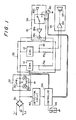
- Fig. 1 is a block diagram of the schematic structure of an embodiment of a side tone preventive circuit for telephones according to the present invention.
- the connecting terminals L1, L2 of the telephone circuit which are connected to an external two-wire telephone circuit, are connected to a rectifier 30 consisting of diodes connected in a bridge.
- the minus connective terminal of the rectifier 30 is grounded and the plus connective terminal thereof is connected to an impedance measuring circuit 32.
- the impedance measuring circuit 32 appropriately measures the impedance of the telephone circuit in response to the instruction from a balance adjustment circuit 34.
- the output side of the impedance measuring circuit 32 is connected to a bridge circuit 36 for side tone prevention.
- a switch 50 is turned on so that a signal is transmitted while bypassing the impedance measuring circuit 32.
- the bridge circuit 36 for side tone prevention includes a telephone internal circuit 12, a balance adjustment circuit 14 and balance impedance elements R9, R10, as in the prior art shown in Fig. 9.
- a receiver 16 and a transmitter 18 are connected to the bridge circuit 36.
- the receiver 16 includes an operational amplifier 16a and a speaker SP.
- the transmitter 18 includes a current amplifier 18a, an operational amplifier 18b and a microphone MIC.
- a switch 38 is inserted between the microphone MIC and the operational amplifier 18b.
- the switch 38 can connect an oscillator 40 to the operational amplifier 18b.
- a switch 44 turns on and off the controller 34.
- the feature of the present invention lies in that the impedance measuring circuit 32 can measure the impedance of the telephone circuit to which the telephone is connected, namely, the circuit impedance Z L . Such measurement of the circuit impedance Z L by the impedance measuring circuit 32 is generally carried out when the telephone is installed.
- a detection circuit 42 is provided.
- the detection circuit 42 is constituted, for example, by an integration circuit consisting of a resistor disposed on the power source side and a capacitor on the grounding side which are connected in series, the integration circuit measuring the potential of the connecting point of the resistor and the capacitor and outputting a pulse when the potential exceeds a predetermined threshold value. Since the integration circuit outputs a pulse only when the voltage of the power source side changes from a low level to a high level, the detection circuit 42 is capable of detecting the connection between the telephone and the telephone circuit. When the detection circuit 42 detects the connection between the telephone and the telephone circuit, the controller 34 is actuated, thereby enabling the measurement of the circuit impedance and the adjustment of the impedance.
- the measurement of the circuit impedance is controlled by the controller 34. More specifically, the switch 38 is changed to the side of the oscillator 40 in response to the instruction of the controller 34, and the oscillator 40 outputs a signal having a predetermined frequency to the telephone circuit. Consequently, the predetermined signal output from the oscillator 40 is output to the telephone circuit, whereby the impedance measuring circuit 32 can measure the circuit impedance Z L .
- the circuit impedance Z L of the telephone circuit measured by the impedance measuring circuit 32 in the above-described way is input to the controller 34.
- the controller 34 determines the resistances and the static capacitance in the balance adjustment circuit 14 by a predetermined calculation based on the circuit impedance Z L of the telephone circuit.
- the resistances and the static capacitance of the balance adjustment circuit 14 are adjusted to the thus-determined values by the operation of the switch or the like in the balance adjustment circuit 14.
- the switch 44 is turned on so as to inhibit the operation of the controller 34, which is unnecessary thereafter.
- the bridge circuit 36 in the present invention is capable of constantly balancing the impedance Z L . Accordingly, it is possible to constantly achieve a good side tone prevention even if the circuit impedance Z L of the external telephone circuit greatly varies.
- a current is applied to a resistor R by turning off a change-over switch 50 so that the impedance measuring circuit is actuated.
- the impedance measuring circuit 32 is provided with a resistor R and two voltmeters 54, 56, so as to measure the voltage V1 of the resistor R on the side of the oscillator 40 and the voltage V2 which has passed the resistor R.
- the switch 38 is operated so as to connect the oscillator 40 to the bridge circuit 36 in place of the transmitter 18.
- the circuit impedance Z L at the frequency f is obtained from the following formula:
- f R/(V1/V2 - 1)
- FIG. 2(A) Another example of the impedance measuring circuit 32 is shown in Fig. 2(A).
- a telephone circuit 52 for operating a telephone as an ordinary telephone is separated by the change-over switch 50 and the oscillator 40 is connected directly to the impedance measuring circuit 32.
- the circuit impedance Z L of the telephone circuit at the connecting terminals L1, L2 of the telephone 300 is schematically represented by Z L .
- the impedance measuring circuit 32 has the resistor R and the two voltmeters 54, 56 as in the impedance measuring circuit 32 shown in Fig. 1.
- the voltmeters 54, 56 measure the voltage V1 of the resistor R on the side of the oscillator 40 and the voltage V2 which has passed the resistor R.
- a voltmeter 60 and an ampere meter 62 are provided in the route from the oscillator 40 to the external telephone circuit, as shown in Fig. 2(B).
- the circuit impedance Z L is obtained from the following formula on the basis of the detected values V and I of the voltmeter 60 and the ampere meter 62, respectively:
- V/I
- the circuit impedance Z L is obtained in the above-described way.
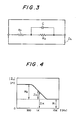
- the circuit impedance Z L consists of a combination of resistance components R1, R2 and a stray capacitance C, as shown in Fig. 3. Calculation of these values will be explained hereinunder.
- the circuit impedance Z L is equivalent to the circuit of a combination of resistors and a capacitor shown in Fig. 3. That is, the circuit composed of the resistor R1, and a parallel connecting circuit of the resistor R2 and the capacitor C which is connected to the resistor R1 in series is equivalent to the circuit impedance Z L . In this kind of circuit, the circuit impedance Z L is different depending upon the frequency f of the signal applied thereto.
- the frequency characteristic of the circuit impedance Z L is shown in Fig. 4.
- a capacitor has a low impedance at a high frequency and a high impedance at a low frequency. Therefore, when the frequency is about 300 H Z , the value of the capacitor C is substantially infinite, while the value of the capacitor C is substantially 0 ⁇ and, hence, the capacitor is short-circuited at a frequency of about 10 kHz, as shown in Fig. 4. Consequently, it is possible to obtain the value of the resistor R1 of the circuit by measuring the circuit impedance Z L at a frequency of 10 kHz.
- R1
- the value of the capacitor C in the circuit impedance Z L is then obtained from the circuit impedance Z L at a frequency of 1 kH Z .
- the circuit impedance Z L at a frequency of 1 kH Z is the impedance of the circuit composed of the resistor R1 and a parallel connecting circuit of the resistor R2 and the capacitor C. It is now assumed that the impedance of the parallel connection circuit of the resistor R2 and the capacitor C is Z c .
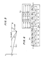
- the locus of the circuit impedance is such as that shown in Fig. 5.
- the circuit impedance Z L is therefore represented by the following formula:
- (R1 + Z c ⁇ cos ⁇ )2 + (Z c ⁇ sin ⁇ )2
- - R12 2 ⁇ R1 ⁇ Z c ⁇ cos ⁇ + Z c 2
- X c ⁇ R22 ⁇ (Z L 2 - R12)/(2 ⁇ R2 ⁇ R2 + R22 -Z L 2 + R12) ⁇ 1/2
- the impedance Z BN of the balance adjustment circuit 36 It is impossible to match the impedance Z BN of the balance adjustment circuit 36 and the impedance of another circuit if the impedance of the telephone internal circuit 12 is also in a predetermined range. If the impedance Z SN of the telephone internal circuit is intended to be set at about 620 ⁇ , a resistor is inserted in the telephone internal circuit at a predetermined position to adjust the impedance.
- the impedance Z BN of the balance adjustment circuit 14 is adjusted in correspondence with these values.
- the resistances and the capacitance of the balance adjustment circuit 14 are adjusted by controlling the groups S1, S2 and S3 of switches appropriately and controlling the connections between resistors R121 to R124, R111 to R114 and capacitors C 131 to C134 , as shown in Fig. 6. For example, if the values of the resistors R121 to R124, R111 to R114 and the capacitors C 131 to C134 are set at 1 : 2 : 4 : 8, respectively, the resistances and the capacitance of the balance adjustment circuit 14 can be set at 1 to 15 times of the respective values.
- the balance adjustment circuit 14 can be constituted by variable resistance elements R12, R11 and R OB , a capacitor C131 and a variable capacity diode (Varicap diode) C132, as shown in Fig. 7.
- the static capacitance of the Varicap diode C132 changes in correspondence with the inverse voltage applied thereto.
- the static capacitance is varied in correspondence with the inverse voltage applied thereto by a variable DC power source E V .
- a coil L13 removes an influence of the impeadance of the variable DC power source E V which applies the voltage to the Varicap diode C132.
- the resistances of the variable resistance elements R12, R11 and R OB are set at predetermined values by the instruction from the controller 34. For example such as those shown in Fig. 8 are adopted as the variable resistance elements R12, R11 and R OB .
- Fig. 8(A) shows a variable resistance element using an LED-CdS (Light Emission Cadmium Sulfide element).
- the resistance of the cadmium sulfide element CdS varies in correspondence with the amount of light emission of the light emission diode LED. Since the amount of light emission of the light emission diode LED varies in correspondence with the amount of current, the resistance of the cadmium sulfide element CdS varies in correspondence with the amount of current. It is therefore possible to control the resistance by varying the amount of current.
- Fig. 8(B) shows a variable resistance element using a Lamp-CdS (Lamp Cadmium Sulfide element).
- Lamp-CdS Lamp Cadmium Sulfide element
- Fig. 8(C) shows a variable resistance element using a MOS-FET (Metal Oxide Semiconductor Field Effect Transistor).
- MOS-FET Metal Oxide Semiconductor Field Effect Transistor
- Fig. 8(D) shows a variable resistance element using a J-FET (Junction-type Field Effect Transistor).
- J-FET Junction-type Field Effect Transistor
- variable resistance element such as those shown in Figs. 8(A) to 8(D)
- the resistances in the balance adjustment circuit 14 become easily adjustable.
- the balance resistors R9 and R10 are adopted, but any impedance elements having a constant ratio can produce the same effect, as is clear from the above formula.
- Fig. 9 shows the side tone preventing characteristic of the bridge circuit in the embodiment.
- the abscissa represents a loss of a signal level (telephone line distance) in the telephone circuit and the ordinate represents a side tone. From Fig. 9, it is clear that a good side tone prevention is constantly carried out irrespective of a change in the loss of a signal level (telephone line distance) in the telephone circuit. In contrast, in the prior art, when the loss of a signal level (telephone line distance) changes, a good side tone prevention is obtained only at one point.
- the adjustment is generally carried out at the time of installation of a telephone, but it may also be carried out when the circuit impedance changes, as occasion demands.
- a good side tone prevention is constantly carried out irrespective of a change in the circuit impedance.
- a side tone preventive circuit for telephones which prevents the output of the transmitter on the speaker's side from being transmitted to the receiver on the same side.
- the balance of the impedance bridge in a bridge circuit for separating a transmission signal and a reception signal is automatically adjusted in accordance with the circuit impedance at the location at which a telephone is installed.
- An impedance measuring circuit measures the impedance of the telephone circuit, and a balance adjustment circuit the impedance of which is adjustable is provided in the bridge circuit.
- the impedance of the telephone circuit is measured at the time of installation of a telephone, and the impedance of the balance adjustment circuit is adjusted in correspondence with the result of measurement.
- the impedance balance of the bridge circuit is adjusted in correspondence with the circuit impedance, thereby effectively preventing a side tone.
Landscapes
- Engineering & Computer Science (AREA)
- Signal Processing (AREA)
- Cable Transmission Systems, Equalization Of Radio And Reduction Of Echo (AREA)
- Telephone Function (AREA)
Abstract
Description
- The present invention relates to an improvement of a side tone preventive circuit for telephones, namely, a circuit for preventing the output of the transmitter on the speaker's side from being transmitted (output) to the receiver on the same side.
- Most of the present telephones are connected to a two-wire telephone circuit, which is divided into a circuit on the receiver's side and a circuit on the transmitter's side by a two-wire four-wire converter consisting of an impedance bridge, and a signal is transmitted. When the balance of the impedance bridge is lost, the output of the transmitter on the speaker's side is transmitted to the receiver on the same side, so that the voice of the speaker is output from the receiver, thereby disturbing a good communication. To prevent such a side tone in a conventional telephone, the impedance balance of the two-wire four-wire converter is controlled.
- The side tone preventive circuit in a conventional telephone will be explained with reference to Fig. 10. In Fig. 10, a
telephone office 100 has an exchanger for connecting a plurality of telephone circuits. The exchanger has onetrunk circuit 10 per telephone circuit connected thereto. The telephone circuit from thetelephone office 100 is connected to atelephone 300 installed in a home or the like throughtelephone lines 200. - The
telephone line 200 is composed of a resistance of the telephone line itself which changes in accordance with the diameter of the line, the distance and the like and a stray capacity which is parasitic on the resistance, as schematically shown in Fig. 10. Thetelephone lines 200 can therefore equivalently represented by resistors, capacitors and the like, as shown in Fig. 10. - The circuit impedance ZL seen from the side of the
telephone 300 is determined by the impedance of thetrunk circuit 10 and thetelephone lines 200 seen from the side of the connecting terminals L₁ and L₂ of thetelephone 300. - The
telephone 300 has aninternal circuit 12 for connecting the connecting terminals L₁ and L₂, and theinternal circuit 12, thetelephone line 200 and thetrunk circuit 10 are connected with each other in parallel. The connecting terminal L₂ is grounded, and balance impedance elements R₉ and R₁₀ for constituting a bridge circuit are connected in series to the connecting terminal L₂. One end of thebalance adjustment circuit 14 is connected to the connecting terminal L₁, and the other end thereof is connected to one end of the balancing resistance R₁₀. In this way, the balancing resistances R₉ and R₁₀, thebalance adjustment circuit 14 and the circuit consisting of theinternal circuit 12 and the external circuit which are connected with each other in parallel constitute an impedance bridge. - A
receiver 16 is provided between the connecting terminal L₂ and the connecting point of the resistor R₁₀ and thebalance adjustment circuit 14, and atransmitter 18 is provided between the connecting point of the resistors R₉ and R₁₀ and the connecting terminal L₁. - Therefore, if the impedance thereof satisfies the following relationship:
(ZL // ZSN) · R₁₀ = ZBN · R₉
the impedance bridge satisfies the balancing condition, so that the output of thetransmittance 18 is not transmitted to thereceiver 16. ZL // ZSN represents the impedance of ZL and ZSN connected in parallel. - In such a conventional impedance bridge, if the above-described balancing condition is satisfied, a sufficiently good side tone prevention is achieved. However, the circuit impedance ZL seen from the side of the
telephone 300 greatly changes in accordance with the diameter of thetelephone line 200 and the distance. As the thetelephone line 200, a line having a diameter of 0.32, 0.4, 0.5, 0.65, 0.9 mm or the like is used, and the loss of the signal level changes by about 0 to 7 dB in accordance with the distance of thetelephone line 200. Therefore, the circuit impedance ZL greatly changes depending upon the state in which thetelephone 300 is installed. However, since thebalance adjustment circuit 14 in aconventional telephone 300 is composed of a stationary CR circuit net, it cannot respond to the impedance ZL of the telephone circuit which greatly changes. - It is at one point in the impedance ZL of the telephone circuit which greatly changes that the impedance bridge satisfies the balancing condition, and the impedance bridge is not balanced under other conditions. Therefore, when the circuit impedance ZL changes, it is impossible to achieve a good side tone prevention.
- Accordingly, it is an object of the present invention to eliminate the above-described problems in the related art and to provide a side tone preventive circuit for telephones which is capable of balancing the impedance bridge so as to obtain a good side tone preventing property under varying telephone circuit conditions.
- To achieve this aim, a side tone preventive circuit for telephones according to the present invention comprises: an impedance measuring circuit which is connected to the connecting terminal of a telephone circuit so as to measure the impedance of the telephone circuit; a bridge circuit for connecting the connecting terminal with a receiver and a transmitter and balancing the impedance at the connecting terminal of the receiver, the bridge circuit including a telephone internal circuit having a predetermined impedance, balance impedance elements and a balance adjustment circuit; and a controller for controlling the impedance of the balance adjustment circuit in accordance with the result of the measurement of the impedance measuring circuit; wherein the balancing condition of the bridge circuit is satisfied by changing the impedance of the balance adjustment circuit in accordance with the measured impedance of the telephone circuit so as to prevent a side tone.
- In the side tone preventive circuit for telephones according to the present invention having the above-described structure, it is possible to measure the impedance of the telephone circuit by the impedance measuring circuit. The impedance of the balance control circuit is controlled on the basis of the result of the measurement. It is therefore possible to constantly balance the bridge circuit even if the circuit impedance of the telephone circuit greatly varies, thereby realizing a good side tone prevention.
- The above and other objects, features and advantages of the present invention will become clear from the following description of the preferred embodiment thereof, taken in conjunction with the accompanying drawings.
-
- Fig. 1 shows the structure of an embodiment of a side tone preventive circuit for telephones according to the present invention;
- Figs. 2(A) and 2(B) show the structures of examples of the impedance measuring circuit in the embodiment shown in Fig. 1;
- Fig. 3 shows an equivalent circuit of a circuit impedance ZL;
- Fig. 4 is a characteristic curve of the frequency characteristic of the circuit impedance ZL;
- Fig. 5 is an explanatory view of the locus of the circuit impedance ZL;
- Fig. 6 is a circuit diagram of an example the balance adjustment circuit;
- Fig. 7 is a circuit diagram of another example the balance adjustment circuit;
- Figs. 8(A) to 8(D) are the circuit diagrams of examples of the structure of a variable resistance element;
- Fig. 9 is a characteristic curve of the side tone preventing property of the embodiment shown in Fig. 1; and
- Fig. 10 shows the structure of a conventional side tone preventive circuit for telephones.
- An embodiment of a side tone preventive circuit for telephones will be explained with reference to the accompanying drawings.
- Fig. 1 is a block diagram of the schematic structure of an embodiment of a side tone preventive circuit for telephones according to the present invention. In Fig. 1, the connecting terminals L₁, L₂ of the telephone circuit, which are connected to an external two-wire telephone circuit, are connected to a
rectifier 30 consisting of diodes connected in a bridge. The minus connective terminal of therectifier 30 is grounded and the plus connective terminal thereof is connected to an impedance measuringcircuit 32. - The impedance measuring
circuit 32 appropriately measures the impedance of the telephone circuit in response to the instruction from abalance adjustment circuit 34. The output side of theimpedance measuring circuit 32 is connected to abridge circuit 36 for side tone prevention. At an ordinary time, when theimpedance circuit 32 is unnecessary, aswitch 50 is turned on so that a signal is transmitted while bypassing theimpedance measuring circuit 32. - The
bridge circuit 36 for side tone prevention includes a telephoneinternal circuit 12, abalance adjustment circuit 14 and balance impedance elements R₉, R₁₀, as in the prior art shown in Fig. 9. Areceiver 16 and atransmitter 18 are connected to thebridge circuit 36. - The
receiver 16 includes anoperational amplifier 16a and a speaker SP. Thetransmitter 18 includes acurrent amplifier 18a, anoperational amplifier 18b and a microphone MIC. In the present invention, aswitch 38 is inserted between the microphone MIC and theoperational amplifier 18b. Theswitch 38 can connect anoscillator 40 to theoperational amplifier 18b. Aswitch 44 turns on and off thecontroller 34. - In the case of holding ordinary communication in a telephone having the above described structure, when the speaker inputs a voice into the microphone MIC of the
transmitter 18, a predetermined current flows on thecurrent amplifier 18a in correspondence with the voice and is output to the telephone circuit through the connecting terminals L₁, L₂. The signal input into the telephone circuit is output from the speaker SP of thereceiver 16 as a voice. - If the impedance of the
bridge circuit 36 satisfies the following balancing condition:
(ZL // ZSN) · R₁₀ = ZBN · R₉
the signal input into thetransmitter 18 is not output from thereceiver 16. - The feature of the present invention lies in that the
impedance measuring circuit 32 can measure the impedance of the telephone circuit to which the telephone is connected, namely, the circuit impedance ZL. Such measurement of the circuit impedance ZL by theimpedance measuring circuit 32 is generally carried out when the telephone is installed. - In this embodiment, a
detection circuit 42 is provided. Thedetection circuit 42 is constituted, for example, by an integration circuit consisting of a resistor disposed on the power source side and a capacitor on the grounding side which are connected in series, the integration circuit measuring the potential of the connecting point of the resistor and the capacitor and outputting a pulse when the potential exceeds a predetermined threshold value. Since the integration circuit outputs a pulse only when the voltage of the power source side changes from a low level to a high level, thedetection circuit 42 is capable of detecting the connection between the telephone and the telephone circuit. When thedetection circuit 42 detects the connection between the telephone and the telephone circuit, thecontroller 34 is actuated, thereby enabling the measurement of the circuit impedance and the adjustment of the impedance. - The measurement of the circuit impedance is controlled by the
controller 34. More specifically, theswitch 38 is changed to the side of theoscillator 40 in response to the instruction of thecontroller 34, and theoscillator 40 outputs a signal having a predetermined frequency to the telephone circuit. Consequently, the predetermined signal output from theoscillator 40 is output to the telephone circuit, whereby theimpedance measuring circuit 32 can measure the circuit impedance ZL. - The circuit impedance ZL of the telephone circuit measured by the
impedance measuring circuit 32 in the above-described way is input to thecontroller 34. Thecontroller 34 determines the resistances and the static capacitance in thebalance adjustment circuit 14 by a predetermined calculation based on the circuit impedance ZL of the telephone circuit. The resistances and the static capacitance of thebalance adjustment circuit 14 are adjusted to the thus-determined values by the operation of the switch or the like in thebalance adjustment circuit 14. - It is preferable that after the
controller 34 is operated once at the time of installment, theswitch 44 is turned on so as to inhibit the operation of thecontroller 34, which is unnecessary thereafter. - In this way, the circuit impedance ZL of the telephone circuit is measured and the resistances and the static capacitance in the
balance adjustment circuit 14 are determined. Thus, thebridge circuit 36 in the present invention is capable of constantly balancing the impedance ZL. Accordingly, it is possible to constantly achieve a good side tone prevention even if the circuit impedance ZL of the external telephone circuit greatly varies. - The measurement of the circuit impedance ZL will now be explained. As a measuring method, a resistance substitution method, a voltage and current measuring method, etc. are known.
- The measurement of the circuit impedance ZL by a resistance substitution method will first be explained with reference to Fig. 1. In this example, a current is applied to a resistor R by turning off a change-
over switch 50 so that the impedance measuring circuit is actuated. - The
impedance measuring circuit 32 is provided with a resistor R and twovoltmeters oscillator 40 and the voltage V₂ which has passed the resistor R. Theswitch 38 is operated so as to connect theoscillator 40 to thebridge circuit 36 in place of thetransmitter 18. When a signal having a predetermined frequency f is transmitted from theoscillator 40, the circuit impedance ZL at the frequency f is obtained from the following formula:
| ZL| f = R/(V₁/V₂ - 1) - Another example of the
impedance measuring circuit 32 is shown in Fig. 2(A). In theimpedance measuring circuit 32 shown in Fig. 2(A), atelephone circuit 52 for operating a telephone as an ordinary telephone is separated by the change-over switch 50 and theoscillator 40 is connected directly to theimpedance measuring circuit 32. In Fig. 2A, the circuit impedance ZL of the telephone circuit at the connecting terminals L₁, L₂ of thetelephone 300 is schematically represented by ZL. - The
impedance measuring circuit 32 has the resistor R and the twovoltmeters impedance measuring circuit 32 shown in Fig. 1. Thevoltmeters oscillator 40 and the voltage V₂ which has passed the resistor R. - In the case of measuring the circuit impedance ZL by a voltage and current measuring method, a
voltmeter 60 and anampere meter 62 are provided in the route from theoscillator 40 to the external telephone circuit, as shown in Fig. 2(B). The circuit impedance ZL is obtained from the following formula on the basis of the detected values V and I of thevoltmeter 60 and theampere meter 62, respectively:
| ZL | = V/I - The circuit impedance ZL is obtained in the above-described way. The circuit impedance ZL consists of a combination of resistance components R₁, R₂ and a stray capacitance C, as shown in Fig. 3. Calculation of these values will be explained hereinunder.
- The circuit impedance ZL is equivalent to the circuit of a combination of resistors and a capacitor shown in Fig. 3. That is, the circuit composed of the resistor R₁, and a parallel connecting circuit of the resistor R₂ and the capacitor C which is connected to the resistor R₁ in series is equivalent to the circuit impedance ZL. In this kind of circuit, the circuit impedance ZL is different depending upon the frequency f of the signal applied thereto.
- The frequency characteristic of the circuit impedance ZL is shown in Fig. 4. A capacitor has a low impedance at a high frequency and a high impedance at a low frequency. Therefore, when the frequency is about 300 HZ, the value of the capacitor C is substantially infinite, while the value of the capacitor C is substantially 0Ω and, hence, the capacitor is short-circuited at a frequency of about 10 kHz, as shown in Fig. 4. Consequently, it is possible to obtain the value of the resistor R₁ of the circuit by measuring the circuit impedance ZL at a frequency of 10 kHz.
R₁ = | ZL| 10k
The circuit impedance ZL at a frequency of 300 Hz is an impedance of the resistor R₁ and the resistor R₂ connected in series. Accordingly, the value of the resistor R₂ is obtained by subtracting the value of resistor R₁ from the circuit impedance ZL at that time:
R₂ = | ZL |₃₀₀ - R₁ - The value of the capacitor C in the circuit impedance ZL is then obtained from the circuit impedance ZL at a frequency of 1 kHZ. As shown in Fig. 4, the circuit impedance ZL at a frequency of 1 kHZ is the impedance of the circuit composed of the resistor R₁ and a parallel connecting circuit of the resistor R₂ and the capacitor C. It is now assumed that the impedance of the parallel connection circuit of the resistor R₂ and the capacitor C is Zc. The locus of the circuit impedance is such as that shown in Fig. 5.
- The circuit impedance ZL is therefore represented by the following formula:
| ZL | = (R1 + Zc · cos ϑ)² + (Zc · sin ϑ)²
By transforming the formula, the following formula is obtained:
| ZL | - R₁² = 2 · R₁ · Zc · cos ϑ + Zc² - Since the resistor R₂ and the capacitor C are connected in parallel, the impedance thereof is represented by the following formula: 1/Zc² = 1/Xc² + 1/R₂²
wherein Xc = | 1/ω · C | - The following relationship holds in the parallel circuit of the resistor R₂ and the capacitor C:
ϑ = tan⁻¹ R₂/Xc - Accordingly, the following relationship is introduced:
cos ϑ = Xc/(Xc² + R₂2)1/2 - Xc is obtained from this relationship equation as follows:
Xc ={ R₂² · (ZL2 - R₁²)/(2 · R₂ · R₂ + R₂² -ZL² + R₁²) } 1/2 - Since ω = 2πf (wherein f represents frequency), the value of the capacitor C is obtained as follows:
C = 1/2πf ·{R₂² · (ZL² - R₁²)/(2 · R₁ · R₂ + R₂² -ZL² + R₁²)} 1/2 - By substituting the value of the circuit impedance ZL at a frequency of 1 kHz (f= 1 kHz) into the above formula, the value of the capacitor C of the bridge circuit is obtained.
- In this way, the circuit impedance ZL is obtained.
- It is impossible to match the impedance ZBN of the
balance adjustment circuit 36 and the impedance of another circuit if the impedance of the telephoneinternal circuit 12 is also in a predetermined range. If the impedance ZSN of the telephone internal circuit is intended to be set at about 620 Ω, a resistor is inserted in the telephone internal circuit at a predetermined position to adjust the impedance. - When the circuit impedance ZL and the impedance ZSN of the telephone
internal circuit 12 are determined, the impedance ZBN of thebalance adjustment circuit 14 is adjusted in correspondence with these values. - The resistances and the capacitance of the
balance adjustment circuit 14 are adjusted by controlling the groups S₁, S₂ and S₃ of switches appropriately and controlling the connections between resistors R₁₂₁ to R₁₂₄, R₁₁₁ to R₁₁₄ and capacitors C131 to C134, as shown in Fig. 6. For example, if the values of the resistors R₁₂₁ to R₁₂₄, R₁₁₁ to R₁₁₄ and the capacitors C131 to C134 are set at 1 : 2 : 4 : 8, respectively, the resistances and the capacitance of thebalance adjustment circuit 14 can be set at 1 to 15 times of the respective values. - The
balance adjustment circuit 14 can be constituted by variable resistance elements R₁₂, R₁₁ and ROB, a capacitor C₁₃₁ and a variable capacity diode (Varicap diode) C₁₃₂, as shown in Fig. 7. In this case, the resistances and the static capacitance are changed by the instruction from thecontroller 34. The static capacitance of the Varicap diode C₁₃₂ changes in correspondence with the inverse voltage applied thereto. The static capacitance is varied in correspondence with the inverse voltage applied thereto by a variable DC power source EV. By a change in the static capacitance of the Varicap diode C₁₃₂, the static capacitance of the series connection circuit of the capacitance C₁₃₁ and the Varicap diode C₁₃₂ is adjusted to a predetermined value. A coil L₁₃ removes an influence of the impeadance of the variable DC power source EV which applies the voltage to the Varicap diode C₁₃₂. - The resistances of the variable resistance elements R₁₂, R₁₁ and ROB are set at predetermined values by the instruction from the
controller 34. For example such as those shown in Fig. 8 are adopted as the variable resistance elements R₁₂, R₁₁ and ROB. - Fig. 8(A) shows a variable resistance element using an LED-CdS (Light Emission Cadmium Sulfide element). In the LED-CdS, the resistance of the cadmium sulfide element CdS varies in correspondence with the amount of light emission of the light emission diode LED. Since the amount of light emission of the light emission diode LED varies in correspondence with the amount of current, the resistance of the cadmium sulfide element CdS varies in correspondence with the amount of current. It is therefore possible to control the resistance by varying the amount of current.
- Fig. 8(B) shows a variable resistance element using a Lamp-CdS (Lamp Cadmium Sulfide element). In the variable resistance element, the amount of light emission varies in correspondence with the amount of current applied to the lamp Lamp, and the resistance of the cadmium sulfide element varies in correspondence with the amount of light emission. It is therefore possible to control the resistance by varying the amount of current.
- Fig. 8(C) shows a variable resistance element using a MOS-FET (Metal Oxide Semiconductor Field Effect Transistor). In the MOS-FET, the resistance between the source and the drain varies in correspondence with the voltage applied to the gate. It is therefore possible to control the resistance by varying the voltage applied to the gate.
- Fig. 8(D) shows a variable resistance element using a J-FET (Junction-type Field Effect Transistor). In this example, it is also possible to control the resistance by varying the voltage applied to the gate as in the case of MOS-FET.
- In this way, if a variable resistance element such as those shown in Figs. 8(A) to 8(D) is adopted, it is possible to control the resistance by an electric signal. It is therefore possible to set the resistance of the variable resistance element at a desired value if an electric signal is generated in accordance with the signal from the
controller 34. It is also possible to adjust the voltage of the variable DC power source EV in accordance with the signal from thecontroller 34, thereby controlling the capacitance of the Varicap diode C₁₃₂. - As an example of the values of the resistors ROB, R₁₁ and R₁₂ and the capacitor C₁₃₁, the following values will be cited from the relationship between the telephone
internal circuit 12 and the impedance ZL: - If the balance resistor R₁₀ adopts 10 times the value of the balance resistor R₉, such as
R₉ = 47 Ω
R₁₀ = 470 Ω
and the resistance of theinternal circuit 12 is set at 620 Ω, the resistance of the resistor ROB in thebalance adjustment circuit 14 is set at
ROB = 10 × ZSN
= 10 × 620 Ω
= 6.2 kΩ - The values of the resistors R₁₂, R₁₁ and the capacitor C₁₃ in the
balance adjustment circuit 14 are set as follows in correspondence with the resistances of the resistors R₁, R₂ and the stray capacitance C, respectively, in the circuit impedance ZL:
R₁₂ = 10 × R₁
R₁₁ = 10 × R₂
C₁₃ = C/10 - In this way, the resistances and the static capacitance in the
balance adjustment circuit 14 are determined and set at these values by the instruction from thecontroller 34. It is therefore possible to so control thebridge circuit 36 as to constantly satisfy the balancing condition by the adjustment of the balance adjustment circuit 14:
(ZL // ZSN) · R₁₀ = ZBN · R₉ - It will also be understood that by appropriately selecting the values of the balance resistors R₉ and R₁₀, the resistances in the
balance adjustment circuit 14 become easily adjustable. In the embodiment, the balance resistors R₉ and R₁₀ are adopted, but any impedance elements having a constant ratio can produce the same effect, as is clear from the above formula. - Fig. 9 shows the side tone preventing characteristic of the bridge circuit in the embodiment. The abscissa represents a loss of a signal level (telephone line distance) in the telephone circuit and the ordinate represents a side tone. From Fig. 9, it is clear that a good side tone prevention is constantly carried out irrespective of a change in the loss of a signal level (telephone line distance) in the telephone circuit. In contrast, in the prior art, when the loss of a signal level (telephone line distance) changes, a good side tone prevention is obtained only at one point.
- Thus, in this embodiment, a constant and good side tone prevention is achieved.
- The adjustment is generally carried out at the time of installation of a telephone, but it may also be carried out when the circuit impedance changes, as occasion demands.
- As described above, according to a side tone preventive circuit for telephones of the present invention, a good side tone prevention is constantly carried out irrespective of a change in the circuit impedance.
- While there has been described what is at present considered to be a preferred embodiment of the invention, it will be understood that various modifications may be made thereto, and it is intended that the appended claims cover all such modifications as fall within the true spirit and scope of the invention.
- A side tone preventive circuit for telephones which prevents the output of the transmitter on the speaker's side from being transmitted to the receiver on the same side. The balance of the impedance bridge in a bridge circuit for separating a transmission signal and a reception signal is automatically adjusted in accordance with the circuit impedance at the location at which a telephone is installed. An impedance measuring circuit measures the impedance of the telephone circuit, and a balance adjustment circuit the impedance of which is adjustable is provided in the bridge circuit. The impedance of the telephone circuit is measured at the time of installation of a telephone, and the impedance of the balance adjustment circuit is adjusted in correspondence with the result of measurement. Thus, the impedance balance of the bridge circuit is adjusted in correspondence with the circuit impedance, thereby effectively preventing a side tone.
Claims (13)
an impedance measuring circuit which is connected to the connecting terminal of a telephone circuit so as to measure the impedance of said telephone circuit;
a bridge circuit for connecting said connecting terminal with a receiver and a transmitter and balancing the impedance at the connecting terminal of said receiver,
said bridge circuit including a telephone internal circuit having a predetermined impedance, balance impedance elements and a balance adjustment circuit; and
a controller for controlling the impedance of said balance adjustment circuit in accordance with the result of the measurement of said impedance measuring circuit;
wherein the balancing condition of said bridge circuit is satisfied by changing the impedance of said balance adjustment circuit in accordance with the measured impedance of said telephone circuit so as to prevent a side tone.
Applications Claiming Priority (4)
| Application Number | Priority Date | Filing Date | Title |
|---|---|---|---|
| JP303300/88 | 1988-11-30 | ||
| JP63303300A JP2848492B2 (en) | 1988-11-30 | 1988-11-30 | Telephone |
| JP63323868A JPH02168761A (en) | 1988-12-22 | 1988-12-22 | Side tone prevention circuit for telephone set |
| JP323868/88 | 1988-12-22 |
Publications (3)
| Publication Number | Publication Date |
|---|---|
| EP0371468A2 true EP0371468A2 (en) | 1990-06-06 |
| EP0371468A3 EP0371468A3 (en) | 1992-05-13 |
| EP0371468B1 EP0371468B1 (en) | 1996-08-28 |
Family
ID=26563479
Family Applications (1)
| Application Number | Title | Priority Date | Filing Date |
|---|---|---|---|
| EP89121970A Expired - Lifetime EP0371468B1 (en) | 1988-11-30 | 1989-11-29 | Side tone preventive circuit for telephone |
Country Status (4)
| Country | Link |
|---|---|
| US (1) | US5029203A (en) |
| EP (1) | EP0371468B1 (en) |
| KR (1) | KR930001816B1 (en) |
| DE (1) | DE68927041T2 (en) |
Cited By (2)
| Publication number | Priority date | Publication date | Assignee | Title |
|---|---|---|---|---|
| EP0581372A3 (en) * | 1992-07-31 | 1994-08-31 | Koninkl Philips Electronics Nv | |
| US5473685A (en) * | 1992-07-31 | 1995-12-05 | U.S. Philips Corporation | Telecommunications end station with electrically controlled terminating impedance |
Families Citing this family (10)
| Publication number | Priority date | Publication date | Assignee | Title |
|---|---|---|---|---|
| KR100288171B1 (en) * | 1992-07-31 | 2001-05-02 | 요트.게.아. 롤페즈 | Terminal for wired telecommunication |
| CA2086573C (en) * | 1992-12-31 | 1996-04-09 | Christopher M. Forrester | Automatic sidetone selector |
| US5533119A (en) * | 1994-05-31 | 1996-07-02 | Motorola, Inc. | Method and apparatus for sidetone optimization |
| US5528685A (en) * | 1994-07-08 | 1996-06-18 | At&T Corp. | Transformerless hybrid circuit |
| KR0143313B1 (en) * | 1995-07-08 | 1998-08-01 | 김광호 | Balanced Network in Key Phone Systems |
| US5892823A (en) * | 1996-03-27 | 1999-04-06 | Hello Direct, Inc. | Smart interface technology |
| US6169762B1 (en) | 1997-05-30 | 2001-01-02 | Lucent Technologies Inc. | Interface devices providing electrical isolation |
| US6151391A (en) * | 1997-10-30 | 2000-11-21 | Sherwood; Charles Gregory | Phone with adjustable sidetone |
| KR100676354B1 (en) * | 2000-03-02 | 2007-01-31 | 산요덴키가부시키가이샤 | Variable resistance circuit, operational amplifier circuit, semiconductor integrated circuit, time constant switching circuit and waveform shaping circuit |
| US8311210B1 (en) * | 2006-06-30 | 2012-11-13 | Plantronics, Inc. | Isolated high gain line amplifier circuit |
Family Cites Families (18)
| Publication number | Priority date | Publication date | Assignee | Title |
|---|---|---|---|---|
| US3462560A (en) * | 1966-04-06 | 1969-08-19 | Bell Telephone Labor Inc | Subscriber telephone circuit with resistance hybrid sidetone balancing network |
| FR1536887A (en) * | 1966-09-12 | Bliss E W Co | Anti-local circuit | |
| US3647982A (en) * | 1970-08-13 | 1972-03-07 | Northern Electric Co | Telephone antisidetone circuit |
| US4081620A (en) * | 1977-05-20 | 1978-03-28 | Bell Telephone Laboratories, Incorporated | Sidetone control circuit for a telephone set |
| US4283675A (en) * | 1979-03-12 | 1981-08-11 | Bell Telephone Laboratories, Incorporated | Impedance/admittance measuring circuit |
| FR2462070A1 (en) * | 1979-07-17 | 1981-02-06 | Cit Alcatel | DEVICE FOR SUPPLYING A SUBSCRIBER STATION |
| US4354060A (en) * | 1979-07-26 | 1982-10-12 | Stromberg-Carlson Corporation | Electronic telephone |
| JPS5651135A (en) * | 1979-10-04 | 1981-05-08 | Nippon Telegr & Teleph Corp <Ntt> | Antiside tone circuit |
| JPS56125145A (en) * | 1980-03-07 | 1981-10-01 | Taiko Denki Seisakusho:Kk | Side tone prevention circuit for telephone set |
| FR2478412A1 (en) * | 1980-03-14 | 1981-09-18 | Radiotechnique Compelec | Automatic impedance appts. for telephone network - momentarily samples impedance magnitude and stores that data to provide stable information to adaptation system |
| US4368361A (en) * | 1980-07-28 | 1983-01-11 | Bell Telephone Laboratories, Incorporated | Automatically adjustable bidirectional-to-unidirectional transmission network |
| GB2130851A (en) * | 1982-11-24 | 1984-06-06 | Grundy & Partners Ltd | Hybrid junction circuits |
| JPH0247907B2 (en) * | 1983-06-15 | 1990-10-23 | Nippon Denshin Denwa Kk | BOSOKUONKAIRO |
| GB8319786D0 (en) * | 1983-07-22 | 1983-08-24 | Plessey Co Plc | Adaptive line hybrids |
| JPS60185452A (en) * | 1984-03-02 | 1985-09-20 | Nippon Telegr & Teleph Corp <Ntt> | Optimum impedance deciding method of side tone preventing circuit |
| US4715064A (en) * | 1984-06-22 | 1987-12-22 | Ncr Corporation | Adaptive hybrid circuit |
| DE3440591C2 (en) * | 1984-11-07 | 1987-01-02 | Neumann Elektronik GmbH, 4330 Mülheim | Device for the optimal adaptation of a hybrid circuit to a telecommunications line |
| JPS61214850A (en) * | 1985-03-20 | 1986-09-24 | Sanyo Electric Co Ltd | Anti-sidetone circuit for telephone set |
-
1989
- 1989-11-27 US US07/441,321 patent/US5029203A/en not_active Expired - Lifetime
- 1989-11-29 DE DE68927041T patent/DE68927041T2/en not_active Expired - Fee Related
- 1989-11-29 EP EP89121970A patent/EP0371468B1/en not_active Expired - Lifetime
- 1989-11-30 KR KR1019890017787A patent/KR930001816B1/en not_active Expired - Fee Related
Cited By (2)
| Publication number | Priority date | Publication date | Assignee | Title |
|---|---|---|---|---|
| EP0581372A3 (en) * | 1992-07-31 | 1994-08-31 | Koninkl Philips Electronics Nv | |
| US5473685A (en) * | 1992-07-31 | 1995-12-05 | U.S. Philips Corporation | Telecommunications end station with electrically controlled terminating impedance |
Also Published As
| Publication number | Publication date |
|---|---|
| EP0371468A3 (en) | 1992-05-13 |
| DE68927041T2 (en) | 1997-02-06 |
| EP0371468B1 (en) | 1996-08-28 |
| KR900011218A (en) | 1990-07-11 |
| KR930001816B1 (en) | 1993-03-13 |
| US5029203A (en) | 1991-07-02 |
| DE68927041D1 (en) | 1996-10-02 |
Similar Documents
| Publication | Publication Date | Title |
|---|---|---|
| EP0371468A2 (en) | Side tone preventive circuit for telephone | |
| HU182505B (en) | Circuit arrangement for setting an interface up between at least one subscriber channel and a digital circuit containing switching matrix | |
| US6124798A (en) | Alarm device designed to warn of danger of hitting high voltage power line by crane in motion | |
| US4315107A (en) | Telephone range extender with gain | |
| US6671371B1 (en) | Adaptive transmit amplifier | |
| US5894262A (en) | Electronic doorbell with reversible diode | |
| US4178569A (en) | Hybrid for two-wire full-duplex transmission of digital signals | |
| US6240177B1 (en) | Communication device comprising an off-hook detection circuit | |
| EP1018028B1 (en) | A device for monitoring partial discharges in an electric high-voltage apparatus or high-voltage equipment | |
| US5668870A (en) | Audible signaling device for informing when a telephone line is available or in use | |
| US5933011A (en) | Ground path testing | |
| IE850335L (en) | Circuit for detecting current variations | |
| EP0486021A2 (en) | Optical receiver | |
| KR100263659B1 (en) | Telephone circuit assembly | |
| US7504853B2 (en) | Arrangement for compensation of ground offset in a data bus system | |
| US4856058A (en) | Office line interface circuits | |
| CA2067535C (en) | Current limited subscriber interface circuit | |
| KR20000068621A (en) | Circuit for controlling a motor with a device for recognising an overload | |
| US5535272A (en) | Sensor circuit for a telephone line | |
| EP1303972B1 (en) | Method of generating a ring signal in a subscriber line interface circuit | |
| US6259298B1 (en) | Method and an arrangement for adapting from a DC point of view a first circuit to at least one second circuit | |
| JP2848492B2 (en) | Telephone | |
| KR810002109B1 (en) | Communication interface circuit | |
| KR0117244Y1 (en) | Analog trunk of private exchange | |
| US5253290A (en) | Circuit arrangement for the transmission of telecommunication signals |
Legal Events
| Date | Code | Title | Description |
|---|---|---|---|
| PUAI | Public reference made under article 153(3) epc to a published international application that has entered the european phase |
Free format text: ORIGINAL CODE: 0009012 |
|
| AK | Designated contracting states |
Kind code of ref document: A2 Designated state(s): DE GB NL |
|
| PUAL | Search report despatched |
Free format text: ORIGINAL CODE: 0009013 |
|
| AK | Designated contracting states |
Kind code of ref document: A3 Designated state(s): DE GB NL |
|
| 17P | Request for examination filed |
Effective date: 19920513 |
|
| 17Q | First examination report despatched |
Effective date: 19940217 |
|
| GRAG | Despatch of communication of intention to grant |
Free format text: ORIGINAL CODE: EPIDOS AGRA |
|
| GRAH | Despatch of communication of intention to grant a patent |
Free format text: ORIGINAL CODE: EPIDOS IGRA |
|
| GRAA | (expected) grant |
Free format text: ORIGINAL CODE: 0009210 |
|
| GRAH | Despatch of communication of intention to grant a patent |
Free format text: ORIGINAL CODE: EPIDOS IGRA |
|
| AK | Designated contracting states |
Kind code of ref document: B1 Designated state(s): DE GB NL |
|
| REF | Corresponds to: |
Ref document number: 68927041 Country of ref document: DE Date of ref document: 19961002 |
|
| PLBE | No opposition filed within time limit |
Free format text: ORIGINAL CODE: 0009261 |
|
| STAA | Information on the status of an ep patent application or granted ep patent |
Free format text: STATUS: NO OPPOSITION FILED WITHIN TIME LIMIT |
|
| 26N | No opposition filed | ||
| PGFP | Annual fee paid to national office [announced via postgrant information from national office to epo] |
Ref country code: GB Payment date: 20011128 Year of fee payment: 13 |
|
| PGFP | Annual fee paid to national office [announced via postgrant information from national office to epo] |
Ref country code: NL Payment date: 20011129 Year of fee payment: 13 |
|
| PGFP | Annual fee paid to national office [announced via postgrant information from national office to epo] |
Ref country code: DE Payment date: 20011217 Year of fee payment: 13 |
|
| REG | Reference to a national code |
Ref country code: GB Ref legal event code: IF02 |
|
| PG25 | Lapsed in a contracting state [announced via postgrant information from national office to epo] |
Ref country code: GB Free format text: LAPSE BECAUSE OF NON-PAYMENT OF DUE FEES Effective date: 20021129 |
|
| PG25 | Lapsed in a contracting state [announced via postgrant information from national office to epo] |
Ref country code: NL Free format text: LAPSE BECAUSE OF NON-PAYMENT OF DUE FEES Effective date: 20030601 |
|
| PG25 | Lapsed in a contracting state [announced via postgrant information from national office to epo] |
Ref country code: DE Free format text: LAPSE BECAUSE OF NON-PAYMENT OF DUE FEES Effective date: 20030603 |
|
| GBPC | Gb: european patent ceased through non-payment of renewal fee | ||
| NLV4 | Nl: lapsed or anulled due to non-payment of the annual fee |
Effective date: 20030601 |