EP0369821A2 - Image processing system - Google Patents
Image processing system Download PDFInfo
- Publication number
- EP0369821A2 EP0369821A2 EP89311956A EP89311956A EP0369821A2 EP 0369821 A2 EP0369821 A2 EP 0369821A2 EP 89311956 A EP89311956 A EP 89311956A EP 89311956 A EP89311956 A EP 89311956A EP 0369821 A2 EP0369821 A2 EP 0369821A2
- Authority
- EP
- European Patent Office
- Prior art keywords
- image
- image data
- signal
- data
- monitor
- Prior art date
- Legal status (The legal status is an assumption and is not a legal conclusion. Google has not performed a legal analysis and makes no representation as to the accuracy of the status listed.)
- Granted
Links
Images


Classifications
-
- H—ELECTRICITY
- H04—ELECTRIC COMMUNICATION TECHNIQUE
- H04N—PICTORIAL COMMUNICATION, e.g. TELEVISION
- H04N1/00—Scanning, transmission or reproduction of documents or the like, e.g. facsimile transmission; Details thereof
- H04N1/387—Composing, repositioning or otherwise geometrically modifying originals
- H04N1/3872—Repositioning or masking
- H04N1/3873—Repositioning or masking defined only by a limited number of coordinate points or parameters, e.g. corners, centre; for trimming
- H04N1/3875—Repositioning or masking defined only by a limited number of coordinate points or parameters, e.g. corners, centre; for trimming combined with enlarging or reducing
Definitions
- the present invention relates to an image processing system and, more particularly, to a processing system for regenerating image data from a medium in which the image data has been stored and forming an image.
- a video signal for television is merely output, and a size of image source of the video signal and the size and output position of the image source of the video signal to an output medium for outputting are also unconditionally determined.
- One of the input image data is merely displayed and output or is printed as a hard copy at a predetermined size and at a predetermined position and its function is limited.
- the signal which is displayed or output to an image processing apparatus such as a television receiver or the like is not limited to the video signals of those apparatuses but an image from an SV record regenerating apparatus or the like or from a personal computer, a work station, a color scanner, or the like also needs to be output to the image processing apparatus.
- the image stored in the SV record regenerating apparatus, a computer, or the like comprises a plurality of image data.
- There is a drawback such that it is impossible to easily select desired one of those plurality of image data and to layout and output the selected image data to an arbitrary or fixed position on an output paper.
- Still another object of the invention is to provide an image processing system which is suitable to select and regenerate a color image.
- an image forming apparatus for receiving image data from a memory apparatus to store image data and forming an image onto an image forming medium
- the apparatus comprises: means for reducing the image data stored in the image memory apparatus; means which can display a plurality of images onto a display image surface by the reducing means and can select a plurality of arbitrary images from the plurality of images displayed; and image forming means for forming images of the image data which were selected by the selecting means and designated in the image memory apparatus to desired positions on the image forming medium.
- Fig. 1 is a system constructional diagram showing an example of a schematic internal construction of a color image forming system of an embodiment according to the invention.
- the system of the embodiment comprises: a digital color image reading apparatus (hereinafter, referred to as a "color reader”) 1 to read a digital color image which is arranged in the upper portion of the system; and a digital color image printing apparatus (hereinafter, referred to as a "color printer”) 2 to print and output a digital color image, an image memory apparatus 3, an SV record regenerating apparatus 31, a monitor television 32, and a host computer 33 which are arranged in the lower portion of the system.
- a digital color image reading apparatus hereinafter, referred to as a "color reader”
- a digital color image printing apparatus hereinafter, referred to as a "color printer”
- the color reader 1 of the embodiment comprises color separating means, which will be explained hereinlater, and a photoelectric converting device which is constructed by a CCD or the like.
- the color reader 1 reads color image data of a read original every color and converts into electric digital image signals.
- the color printer 2 is a laser beam color printer of the electrophotographic type in which color images are limited every color in accordance with the digital image signal to be output and are copy transferred onto a recording paper a plurality of times in a digital dot form and recorded.
- the image memory apparatus 3 is an apparatus in which a read digital image from the color reader 1 is stored or an analog video signal from the SV record regenerating apparatus 31 is digitized and converted into a digital image and, thereafter, the digital image is stored.
- the SV record regenerating apparatus 31 is an apparatus in which images are photographed by an SV camera and the image data recorded in a SV floppy is regenerated and output as an analog video signal. On the other hand, the SV record regenerating apparatus 31 can receive an analog video signal and can also record into an SV floppy in addition to the above functions.
- the monitor television 32 displays images stored in the image memory apparatus 3 and also displays the content of the analog video signal output from the SV record regenerating apparatus 31.
- the host computer 33 has functions to transmit the image data to the image memory apparatus 3 and to receive the image data from the color reader 1 or the SV record regenerating apparatus which has been stored in the image memory apparatus 3.
- the host computer 33 also controls the color reader 1 and color printer 2 and the like.
- reference numeral 999 denotes an original
- 4 indicates a platen glass onto which an original is put
- 5 represents a rod array lens for converging a reflected light image from the original which was exposed and scanned by a halogen exposure lamp 10 and for inputting the image into an equal size type full color sensor 6.
- the rod array lens 5, the full color sensor 6, a sensor output signal amplifying circuit 7, and the halogen exposure lamp 10 integrally construct an original scanning unit 11.
- the scanning unit 11 exposes and scans the original 999 in the direction indicated by an arrow (A1).
- the image data of the original 999 to be read is sequentially read every line by exposing and scanning the original scanning unit 11.
- the read color separation image signal is amplified to a predetermined voltage by the sensor output signal amplifying circuit 7. Thereafter, it is input to a video processing unit via a signal line 501 and processed.
- the signal line 501 is constructed as a coaxial cable to guarantee the signal transmission with a high fidelity.
- Reference numeral 502 denotes a signal line to supply drive pulses of the equal size type full color sensor 6. All of the necessary drive pulses are produced in a video processing unit 12.
- Reference numerals 8 and 9 denote a white plate and a black plate to correct the white and black levels of the image signal. Signal levels of predetermined concentrations can be obtained by irradiating the white plate 8 and the black plate 9 by the halogen exposure lamp 10, respectively, and are used to correct the white and black levels of the video signal.
- Reference numeral 13 denotes a control unit to control the whole color reader 1 of the embodiment having a microcomputer.
- the control unit 13 executes the display on an operation panel 20, the control of key inputs, the control of the video processing unit 12, and the like through a bus 508.
- the control unit 13 detects the position of the original scanning unit 11 through signal lines 509 and 510 on the basis of detection signals by position sensors S1 and S2.
- control unit 13 executes all of the controls in the color reader 1. That is, the control unit 13 controls a stepping motor drive circuit 15 to pulse drive a stepping motor 14 to move the scanning unit 11 through a signal line 503.
- the control unit 13 controls the on/off operations and a light amount of the halogen exposure lamp 10 by an exposure lamp driver 21 through a signal line 504.
- the control unit 13 controls a digitizer 16, internal keys, the display section, and the like through a signal line 505.
- the color image signal which was read by the exposure scanning unit 11 upon exposing and scanning of the original is input to the video processing unit 12 through the sensor output signal amplifying circuit 7 and the signal line 501.
- the color image signal input to the video processing unit 12 is separated into three color signals of G (green), B (blue), and R (red) by a sample and hold circuit S/H 43.
- the separated color image signals are analog processed by an analog color signal processing circuit 44 and, thereafter, they are A/D converted into the digital color image signals.
- the color reading sensor 6 in the original scanning unit 11 is constructed in a zigzag shape which is divided into five areas as also shown in Fig. 2. Deviations of the reading positions among the channels 2 and 4 which have previously been scanned and the remaining channels 1, 3, and 5 are corrected by using the color reading sensor 6 and an FIFO memory 46. The signals after the positional deviations were corrected which are output from the FIFO memory 46 are input to a black correction/white correction circuit 85. A variation in the dark state of the sensor 6, a variation in light amount of the lamp 10, a variation in sensitivity of the sensor, and the like are corrected by using the signals corresponding to the reflected lights from the white plate 8 and black plate 9 mentioned above.
- the color image data which is proportional to the input light amount of the color sensor 6 is input to a video interface 101 and connected to the image memory apparatus 3.
- the video interface 101 has the following four functions as shown in Figs. 3 to 6: that is,
- the reading (fetching) control in the color reader 1 and the storage control of the read image data into the image memory apparatus 3 in the embodiment will now be described.
- Fig. 7 shows an external view of the digitizer 16.
- reference numeral 427 denotes an entry key to transfer the image data from the color reader 1 to the image memory apparatus 3.
- a coordinate detecting plate 420 is used to set an arbitrary area on the reading original or to set a reading magnification or the like.
- a point pen 421 is used to designate the coordinates of the pen.
- the entry key 427 in Fig. 7 is depressed and, thereafter, a reading position is indicated by the point pen 421.
- the image data of the reading area is sent to the video processing unit 12 through the communication line 505 in Fig. 1.
- the video processing unit 12 transmits the input image signal from the video interface 101 to the image memory apparatus 3 by the CPU control line 508.
- the color reader 1 After the entry key 427 in Fig. 7 was depressed, if a reading position is not indicated by the point pen 421, the color reader 1 detects a size of original 999 by the prescan and transmits the size data as image reading area information to the image memory apparatus 3 through the video interface 101.
- Fig. 8 shows an example of addresses of the information (points A and B) of the area indicated by the point pen 421 of the digitizer 16.
- the video interface 101 outputs not only the area information but also a VCLK signal, an ITOP signal 551, an EN signal 104 as a signal from an area signal generation circuit 51, and the like to the image memory apparatus 3 together with the image data.
- Fig. 9 shows a timing chart for those output signal lines.
- the stepping motor 14 is driven and the original scanning unit 11 starts the scanning.
- the ITOP signal 551 is set to the "1" level.
- the scanning unit 11 reaches the area designated by the digitizer 16.
- the EN signal 104 is held at the "1" level. Therefore, it is sufficient to input the read color image data (DATA 105, 106, and 107) when the EN signal 104 is set to "1".
- the R data 105, G data 106, and B data 107 are transmitted to the image memory apparatus 3 in a real-time manner synchronously with the ITOP signal 551, control signal of the EN signal 104, and VCLK signal.
- a connector 4550 is connected to the video interface 101 of the color reader 1 through a cable.
- the R data 105, G data 106, and B data 107 are connected to a selector 4250 through signal lines 9430R, 9430G, and 9430B, respectively.
- the VCLK signal, EN signal 104, and ITOP signal 551 which are sent from the video interface 101 pass through a signal line 9450 and are directly input to a system controller 4210.
- the area information designated by the digitizer 16 passes through a communication line 9460 and is input to a reader controller 4270.
- the area information is output from the reader controller 4270 to a CPU 4360 through a CPU bus 9610.
- the R data 105, G data 106, and B data 107 which were input to the selector 4250 through the signal lines 9430R, 9430C, and 9430B are selected by the selector 4250 and, thereafter, they are output to signal lines 9420R, 9420C, and 9420B and are input to FIFO memories 4050R, 4050G, and 4050B, respectively.
- Fig. 11 shows a detailed constructional diagram of the selector 4250.
- a control signal SELECT-A 9451A from the system controller 4210 is set to 1
- a control signal SELECT-B 9451B is set to 1
- a control signal SELECT-C 9451C is set to 0.
- Only tristate buffers 4251E, 4251V, 4251R, 4251G, and 4215B are made operative and other tristate buffers 4255E, 4255V, 4255R, 4255G, 4255B, 4256E, 4256V, 4256R, 4256G, and 4256B are set to the high impedance, respectively.
- the VCLK signal and EN signal in the control signal 9450 are also selected by the SELECT signals 9451A, 9451B, and 9451C.
- the VCLK signal and EN signal are the signals which are output from the color reader 1. Only the tristate buffers 4251E and 4251V are made operative. Thus, those signals pass through signal lines CLKIN 9456 and ENIN 9457 and are input to the system controller 4210.
- control signals VSYNCIN 9455 and HSYNCIN 9452 are directly input from the connector 4550 to the system controller 4210.
- the selector 4250 also has the function to average the image data from the color reader 1.
- the signals 9430R, 9430G, and 9430B which are input from the color reader pass through signal lines 9421R, 9421G, and 9421B and are input to FIFO memories 4252R, 4252G, and 4252B.
- Outputs from the FIFO memories 4252R, 4252G, and 4252B are the signals which are delayed by one main scanning period than the image data 9421R, 9421G, and 9421B and pass through signal lines 9422R, 9422G, and 9422B and are input to adders 4253R, 4253G, and 4253B.
- the signals 9421R, 9421G, and 9421B from the tristate buffers 4251R, 4251G, and 4251B are input to the adders 4253R, 4253G, and 4253B.
- the adders 4253R, 4253G, and 4253B each calculate the mean value of total four pixels comprising two pixels in the main scanning direction and two pixels in the subscanning direction and output to signal lines 9423R, 9423G, and 9423B.
- Selectors 4254R, 4254G, and 4254B select either the image signals 9421R, 9421G, and 9421B from the color reader 1 or the weighted mean signals 9423R, 9423G, and 9423B and output the signals 9420R, 9420G, and 9420B into the FIFO memories 4050R, 4050G, and 4050B.
- the system controller 4210 transfers only the effective area of the image among the image data 9420R, 9420G, and 9420B from the selectors 4254R, 4252G, and 4254B into the FIFO memories 4050R, 4050G, and 4050B. On the other hand, at this time, the system controller 4210 also simultaneously executes the trimming process and the variable magnifying process.
- FIFO memories 4050R, 4050G, and 4050B eliminate the differences of the clocks between the color reader 1 and the image memory apparatus 3.
- a start address in the main scanning direction of the area designated by the digitizer 16 is set into the comparator 4232, while a stop address is set into the comparator 4233.
- the CPU bus 9610 side is selected and is made effective by controlling a selector 4213.
- the "0" data is written into the effective area of the area designated in an RAM 4212, while the "1" data is written into the ineffective area.
- variable magnifying process in the main scanning direction a variable magnification ratio is set into a rate multiplier 4234 through the CPU bus 9610.
- the variable magnifying process in the subscanning direction can be realized by the data which is written into the RAM 4212.
- Fig. 13 is a timing chart in the case of executing the trimming process.
- the trimming position in the main scanning direction is set into the comparators 4232 and 4233 and the trimming position in the subscanning direction is written into the RAM 4212 by the CPU by switching the selector 4213 to the side of the CPU bus 9610 ((for instance) trimming area: main scan 1000 to 3047; subscan 1000 to 5095).
- a trimming interval signal 9100 in the main scanning direction when a counter 4230 operates synchronously with the HSYNCIN signal 9452 and CLKIN signal 9456 and a counter output 9103 is set to 1000, the output of the comparator 4232 is set to 1 and a Q output of a flip-flop 4235 is set to 1. Subsequently, when the counter output 9103 is set to 3047, the output of the comparator 4233 is set to 1 and the output of the flip-flop 4235 is set from 1 to 0. On the other hand, in the timing chart of Fig. 13, since the equal size magnifying process is executed, an output of the rate multiplier 4234 is set to 1.
- the image data in addresses 1000 to 3047 in the color image data which is input into the FIFO memories 4050R, 4050G, and 4050B by the trimming interval signal 9100 is written into the FIFO memories 4050R, 4050G, and 4050B.
- a comparator 4231 outputs a signal 9102 which is delayed by pixels than the HSYNCIN signal 9452.
- the providing the phase difference between the signals which are input to RSTW and RSTR input terminals of each of the FIFO memories 4050R, 4050G, and 4050B, the difference between the periods of the CLKIN signal 9456 and the CLK signal 9453 which are input to the FIFO memories 4050R, 4050G, and 4050B is eliminated.
- a counter 4214 side is first selected and is made effective by controlling the selector 4213 and an interval signal 9104 synchronized with the VSYNCIN signal 9455 and HSYNCIN signal 9452 is output from the RAM 4212.
- the interval signal 9104 is synchronized with the signal 9102 by a flip-flop 4211 and is input to a reset read ( RE ) input terminal of each of the FIFO memories 4050R, 4050G, and 4050B. That is, the image data stored in the FIFO memories 4050R, 4050G, and 4050B is output (n′ - m′) only for the interval when a trimming signal 9101 is set to "0".
- variable magnifying process can be also executed simultaneously with the trimming.
- a variable magnification ratio is set into the rate multiplier 4234 through the CPU bus 9610.
- the variable magnifying process in the subscanning direction can be realized on the basis of the data which is written into the RAM 4212.
- Fig. 14 shows a timing chart in the case where the trimming process and the variable magnifying process (50%) were executed.
- Fig. 14 is a diagram showing an example of the timing chart in the case where the image data from the selectors 4254R, 4254G, and 4254B are reduced by 50% by executing the variable magnifying process and the reduced image data are transferred to the FIFO memories 4050R, 4050G, and 4050B.
- the variable magnification ratio of 50% reduction is set into the rate multiplier 4234 in Fig. 12 through the CPU bus 9610.
- an output 9106 of the rate multiplier 4234 has a waveform such that "0" and "1” are repeated every pixel in the main scanning direction as shown in Fig. 14.
- the AND signal 9100 of the output signal 9106 of the rate multiplier 4234 and an interval signal 9105 formed by the comparators 4232 and 4233 is used to control the write enable operation to the FIFO memories 4050R, 4050G, and 4050B, thereby executing the reduction.
- the write enable operations of the FIFO memories 4050R, 4050G, and 4050B are controlled.
- the read enable operations of the FIFO memories 4050R, 4050G, and 4050B are controlled.
- the image data transfer from the FIFO memories 4050R, 4050G, and 4050B to the memories 4060A, 4060G, and 4060B is executed by a counter 0 (4080-0) and control line 9101.
- the control line 9101 corresponds to the read enable signal of the FIFO memories 4050A, 4050G, and 4050B, the enable signal of the counter 4080-0, and the write enable signal of the memories 4060R, 4060G, and 4060B.
- the image data which was read out of the FIFO memories 4050R, 4050G, and 4050B passes through tristate buffers 9090R, 9090G, and 9090B and is input to the memories 4060R, 4060G, and 4060B.
- the enable signal of the counter 4080-0 is also set to "0".
- a count-up signal 9120-0 is output from the counter 4080-0 synchronously with a CLK signal 9453 and passes through a selector 4070 and is input to an ADR 9110 of each of the memories 4060A, 4060G, and 4060B.
- the write enable WE signal 9101 of the memories 4060R, 4060G, and 4060B is also set to "0"
- the image data 9090R, 9090G, and 9090B which are input to the memories 4060R, 4060G, and 4060B are stored.
- the memory capacity of each color is set to 1 Mbytes. Therefore, by reducing the image data of the read area in Fig. 8 by 50%, the read image data is converted into the data of the maximum capacity of each memory provided in the image memory apparatus 3 and is stored.
- the CPU 4360 calculates the effective area from the information of the area of the original of the A3 size which was designated by the digitizer 16. The CPU 4360 then sets the data corresponding to the comparators 4231 to 4233, rate multiplier 4234, and RAM 4212.
- the reducing process is executed and the image data is converted into the small data of the capacity which can be stored and, thereafter, it is stored into the image memory.
- the capacity of the read image data is smaller than the image memory capacity, by setting a CLR signal 9171 in Fig. 15 to "1", a plurality of image surfaces can be simultaneously stored into the image memory.
- the trimming data is set into the comparators 4232 and 4233 to control the writing of the area designated by the digitizer 16 to the memory and the equal size mode is set into the rate multiplier 4234.
- the write data to the RAM 4212 all of the image effective areas are set to "0" and the other areas are set to "1" and the equal size is set.
- an arbitrary variable magnifying process can be easily executed by merely controlling the inside of the image memory apparatus 3 while keeping the aspect ratio of the input image.
- the read image can be effectively recognized.
- the using efficiency of the memory capacity can be set to the maximum value.
- the system of the embodiment can not only store the video image from the SV record regenerating apparatus 31 into the image memory apparatus 3 but also output to the monitor television 32 or the color printer 2.
- the image processing apparatus 3 also executes the handling of the input image.
- the video image from the SV record regenerating apparatus 31 is input in a form of an NTSC composite signal 9000 through an analog interface 4500 and is separated into four signals 9015R, 9015G, 9015B, and 9015S (these signals are generally referred to as 9015) comprising separate R, G, B signals and a composite SYNC signal by a decoder 4000.
- the decoder 4000 also decodes Y (luminance)/C (chrominance) signals 9010 from an analog interface 4510 in a manner similar to the above.
- Signals 9020R, 9020G, 9020B, and 9020S are input to a selector 4010 in a form of the separate R, G, and B signals and the composite SYNC signal.
- a switch 4530 is provided to control the selector 4010 for selecting and switching either the input signals 9020R, 9020G, 9020B, and 9020S or the signals 9015R, 9015G, 9015B, and 9015S.
- the switch 4530 When the switch 4530 is open, the signals 9020R to 9020S are selected.
- the switch 4530 is closed, the signals 9015R to 9015S are selected.
- R, G, and B signals 9050R, 9050G, and 9050B selected by the selector 4010 are analog/digital converted into digital signals by A/D converters 4020R, 4020G, and 4020B.
- a selected composite SYNC signal 9050S is input to a TBC/HV separation circuit 4030.
- a clock signal 9060C, a horizontal sync signal 9060H, and a vertical sync signal 9060V are produced from the composite SYNC signal 9050S by the TBC/HV separation circuit 4030. Those sync signals are supplied to the system controller 4210.
- the TVCLK signal 9060C which is output from the TBC/HV separation circuit 4030 in the embodiment is the clock signal of 12.25 MHz
- the TVHSYNC signal 9060H is the signal of a pulse width of 63.5 ⁇ sec
- the TVVSYNC signal 9060V is the signal of a pulse with of 16.7 msec.
- the FIFO memories 4050R, 4050G, and 4050B are reset by the TVHSYNC signal 9060H and data 9060R, 9060G, and 9060B are written into the FIFO memories from address "0" synchronously with the TVCLK signal 9060C. At this time, the writing operations to the FIFO memories 4050R, 4050G, and 4050B are executed when the WE signal 9100 which is output from the system controller 4210 is set to "1".
- the SV record regenerating apparatus 31 in the embodiment is based on the NTSC standard. Therefore, when the video image from the SV record regenerating apparatus 31 is digitized, the image surface capacity is set to 640 pixels (in the horizontal direction: H) x 480 pixels (in the vertical direction: V). Therefore, the CPU 4360 of the image memory apparatus 3 first writes set values into the comparators 4232 and 4233 so that the number of pixels in the main scanning direction is set to 640. Next, the CPU 4360 switches the input signals of the selector 4213 to the CPU bus 9610 side and writes "0" data as many as 480 pixels in the subscanning direction into the RAM 4212.
- the data of 100% is set into the rate multiplier 4234 to set the magnification in the main scanning direction.
- the system controller 4210 connects the TVVSYNC signal 9060V, TVHSYNC signal 9060H, and TVCLK signal 9060V which are output from the TBC/HV separation circuit 4030 to the VSYNCIN signal 9455, HSYNCIN signal 9452, and CLKIN signal 9456 shown in Fig. 12.
- the data of the single main scan of the video images of the output signals 9060R, 9060G, and 9060G from the A/D converters 4020R, 4020G, and 4020B are stored into the FIFO memories 4050R, 4050G, and 4050B at the equal size.
- the reduction ratio is set into the rate multiplier 4234 and the data in the RAM 4212 in the image effective area is set to "1" in accordance with the reduction ratio, so that the video image can be reduced.
- the data transfer from the FIFO memories 4050R, 4050G, and 4050B to the memories 4060R, 4060G, and 4060B is executed in a manner similar to the case of the data writing control from the color reader 1 to the memories 4060R, 4060G, and 4060B mentioned above.
- the SV record regenerating apparatus 31 in the embodiment is based on the NTSC standard.
- the invention can be also applied to the aspect ratio of 16:9 of the HDTV standard which is presumed as the standard of the future television.
- the memory capacity in the embodiment has been set to 2 Mbytes.
- the capacity of one image surface of the NTSC standard is set to about 0.3 Mbytes, the images of six image surfaces can be stored. Such storage of six image surfaces can be also realized by setting the CLR signal 9171 shown in Fig. 15 to "1".
- one image surface can be stored into the memory of 2 Mbytes.
- the invention can also cope with the realization of the high band of the video apparatuses. That is, by raising the TVCLK clocks which are output from the TBC/HV separation circuit 4030 in the embodiment, the number of read pixels in the main scanning direction can be increased.
- a command input and the like in the case where an image is formed by the color printer 2 on the basis of the image outputs from the memories are mainly executed by the digitizer 16 shown in Fig. 7 mentioned above.
- reference numeral 428 denotes an entry key for allowing the color printer 2 to form an image onto a recording paper in accordance with the size of recording paper on the basis of the image data from the memories 4060R, 4060G, and 4060B.
- Reference numeral 429 indicates an entry key for allowing an image to be formed at the position designated by the coordinate detecting plate 420 of the digitizer 16 and by the point pen 421.
- the color printer 2 has two cassette trays 735 and 736 and two kinds of recording papers are set.
- the recording papers of the A4 size are set to the upper stage and the recording papers of the A3 size are set to the lower stage.
- An instruction to select the recording papers is input by a liquid crystal touch panel in the operation unit 20.
- the following description relates to the case of forming a plurality of images onto the recording paper of the A4 size.
- the entry key 428 of the digitizer 16 is pressed.
- the CPU (not shown) detects such a key input and automatically sets the image forming position to the recording paper of the A4 size.
- the image forming position is set as shown in Fig. 17.
- An ITOP signal 511 which is sent from the color printer 2 shown in Fig. 2 to the color reader 1 through the printer interface 56 is input to the video interface 101 in the video processing unit 12.
- the ITOP signal is then sent from the video interface 101 to the image memory apparatus 3.
- the image memory apparatus 3 starts the image forming process in response to the ITOP signal 551.
- Each image sent to the image memory apparatus 3 is formed under the control of the system controller 4210 shown in Figs. 10A and 10B in the image memory apparatus 3.
- an output of the counter 0 (4080-0) is selected by the selector 4070.
- the memories 4060R, 4060G, and 4060B are accessed to read by a memory address line 9110. Due to the access, the image data stored in the memories 4060R, 4060G, and 4060B are read out.
- Image signals 9160R, 9160G, and 9160B which were read out of the memories are transferred to look-up tables (LUT) 4110R, 4110G, and 4110B, by which logarithm conversion to match with the relative luminous efficiency characteristics of the human eyes is executed.
- Conversion data 9200R, 9200G, and 9200B from the LUT are input to a masking/black extraction/UCR circuit 4120.
- the color correction of the color image signals in the image memory apparatus 3 is executed by the masking/black extraction/UCR circuit 4120 and the UCR/black extraction processes are also executed in the black recording mode.
- a sequential image signal 9210 from the masking/black extraction/UCR circuit 4120 is separated every image by a selector 4130.
- the separated signals are input to FIFO memories 4140-0 to 4140-3.
- the images which have sequentially been arranged so far can be processed in parallel by the functions of the FIFO memories 4140-0 to 4140-3.
- the parallel image signals 9260-0 to 9260-3 are input to enlargement/interpolation circuits 4150-0 to 4150-3 at the next stage.
- the circuits 4150-0 to 4150-3 are controlled by the system controller 4210 so as to obtain a layout of the images shown in Fig. 17 and execute the enlargement/interpolation processes as shown by signals 9300-0 to 9300-3 in Fig. 18. In the embodiment, the primary interpolating method is used.
- the interpolated signals 9300-0 to 9300-3 are input to a selector 4190.
- the image data which were processed in parallel so far are again converted into the serial image data signal.
- An image signal 9330 converted into the serial image data by the selector 4190 is subjected to an edge emphasizing process and a smoothing process by an edge filter circuit 4180.
- the processed image signal passes through an LUT 4200 and is input to the selector 4250 through a signal line 9380.
- the signals input to the selector 4250 pass through the tristate buffers 4256R, 4256G, 4256B, 4255R, 4255G, and 4255B and are output to the connector 4550 through the signal lines 9430R, 9430G, and 9430B.
- an ENOUT signal 9454 and the CLK signal 9453 which are output from the system controller 4210 also pass through the tristate buffers 4256E, 4256V, 4255E, and 4255V and are output to the connector 4550 through the signal line 9450.
- control lines SELECT-A 9451A, SELECT-B 9451-B, and SELECT-C 9451-C to control the gates of the tristate buffers shown in Fig. 11 are set to "0", "0" and "1", respectively.
- the embodiment is not limited to the above example but images can be also formed by developing arbitrary images to arbitrary positions.
- desired developing positions are designated and input by the coordinate detecting plate 420.
- the developing areas are designated and input as shown in Fig. 20.
- Fig. 21 is a timing chart in the case of forming the image at line "l1" shown in Fig. 20.
- Fig. 22 is a timing chart in the case of forming the image at line "l2" in Fig. 20.
- the ITOP signal 551 is output from the color printer 2 in a manner similar to the above and the system controller 4210 starts the operation synchronously with the signal.
- image 3 is obtained by rotating the image from the color reader 1 by 90°.
- the image rotating process is executed in the following procedure. First, the images are transferred from the memories 4060R, 4060G, and 4060B to a work memory 4390 by a DMAC (direct memory access controller) 4380 in Figs. 10A and 10B. Next, after the well-known image rotating process was executed in the work memory 4390 by the CPU 4360, the images are transferred from the work memory 4390 to the memories 4060R, 4060G, and 4060B by the DMAC 4380, so that the image rotating process is executed.
- a DMAC direct memory access controller
- the position data of the images which were laid out and indicated and input by the digitizer 16 are sent to the image memory apparatus 3 through the video processing unit 12 in Fig. 1.
- the system controller 4210 receives the developing position data for the images, the system controller generates operation permission signals 9320-0 to 9320-3 of the enlargement/interpolation circuits 4150-0 to 4150-3 corresponding to the images.
- the counter 0 (4080-0) operates in correspondence to "image 0"
- a counter 1 (4080-1) operates in correspondence to "image 1”
- a counter 2 (4080-2) operates in correspondence to "image 2”
- a counter 3 (4080-3) operates in correspondence to "image 3", respectively.
- the counters 4080-2 and 4080-3 are not operative by counter enable signals 9130-2 and 9130-3 from the system controller 4210.
- the image data of "image 0" and “image 1" are sent to the masking/black extraction/UCR circuit 4120 through the LUT 4110R, 4110G, and 4110B and are converted into the area sequential color signal 9210.
- the area sequential color signal 9210 is converted into the parallel signals by the selector 4130 and separated every pixel and sent to the FIFO memories 4140-0 and 4140-1.
- the circuits 4150-0 and 4150-1 set FIFO readout signals 9280-0 and 9280-1 to the enable state, thereby starting the reading control.
- the FIFO memories 4140-0 and 4140-1 start the transfer of the image data to the enlargement/interpolation circuits 4150-0 and 4150-1.
- the layout and interpolating calculations of the images are executed by the enlargement/interpolation circuits 4150-0 and 4150-1 in accordance with the area designated by the digitizer 16. The timings for those operations are shown by 9300-0 and 9300-1 in Fig. 21.
- the practical control method is similar to that in the case mentioned above.
- Signals from the connector 4550 are connected to the color reader 1 by the cable. Therefore, the video interface 101 of the color reader 1 selects and outputs the image signal 105 from the image memory apparatus 3 to the printer interface 56 via the signal line path shown in Fig. 5.
- the printer 2 starts operating and starts the conveyance of the recording paper.
- the ITOP signal 551 is output.
- the ITOP signal 551 is sent to the image memory apparatus 3 through the color reader 1.
- the image memory apparatus 3 reads out the image data stored in the image memories 4060R, 4060G, and 4060B and these image data are subjected to the processes for the layout, enlargement/interpolation, and the like mentioned above and, thereafter, the processed image data is sent to the video processing unit 12 of the color reader 1.
- the video interface 101 of the video processing unit 12 changes the processing method in the video interface 101 in accordance with the kind (R, G, B)/(M, C, Y, Bk) of the data transmitted.
- reference numeral 711 denotes a scanner having: a laser output unit to convert the image signal from the color reader 1 into the photo signal; a polygon mirror 712 of a polyhedron (for instance, octahedron); a motor (not shown) to rotate the polygon mirror 712; an f/ ⁇ lens (image forming lens) 713; and the like.
- Reference numeral 714 denotes a reflecting mirror to change the optical path of the laser beam from the scanner 711 shown by an alternate long and short dash line in the diagram, and 715 indicates a photo sensitive drum.
- the laser beam emitted from the laser output unit is reflected by the polygon mirror 712 and scans (raster scan) like a line on the surface of the photo sensitive drum 715 by the f/ ⁇ lens 713 and reflecting mirror 714, thereby forming an electrostatic latent image corresponding to the original image.
- Reference numeral 717 denotes a primary charging device; 718 indicates a whole surface exposure lamp; 723 a cleaner unit to collect the residual toner which was not copy transferred; and 724 a copy transfer precharging device. Those parts are arranged around the photo sensitive drum 715.
- Reference numeral 726 denotes a developing unit to develop the electrostatic latent image formed on the surface of the photo sensitive drum 715 by the laser exposure; 731Y (for yellow), 731M (for magenta), 731C (for cyan), and 731Bk (for black) indicate developing sleeves which are come into contact with the photo sensitive drum 715 and directly execute the development; 730Y, 730M, 730C, and 730Bk toner hoppers to hold spare toners; and 732 a screw to transfer a developing agent.
- the developing unit 726 is constructed by the sleeves 731Y to 731Bk, toner hoppers 730Y to 730Bk, and screw 732. Those parts are arranged around a rotary shaft P of the developing unit 726.
- the yellow toner development is executed at the position shown in the diagram.
- the developing unit 726 is rotated around the shaft P as a rotational center in the diagram, thereby setting the developing sleeve 731M in the magenta developing unit to the position where the sleeve 731M is come into contact with the photo sensitive drum 715.
- the developing unit 726 is also rotated around the shaft P in the diagram as a rotational center and is made operative in a manner similar to the above.
- reference numeral 716 indicates a copy transfer drum to copy transfer the toner image formed on the photo sensitive drum 715 onto the recording paper.
- Reference numeral 719 indicates an actuator plate to detect the moving position of the copy transfer drum 716; 720 a position sensor to detect that the copy transfer drum 716 has moved to the home position by approaching to the actuator plate 719; 725 a copy transfer drum cleaner; 727 a paper pressing roller; 728 a discharging device; and 729 a copy transfer charging device.
- the above parts 719, 720, 725, 727, and 729 are arranged around the copy transfer drum 716.
- reference numerals 735 and 736 denote the paper feed cassettes to collect the papers (cut sheets); 737 and 738 indicate paper feed rollers to feed the papers from the cassettes 735 and 736; and 739, 740, and 741 represent timing rollers to match the timings for the paper feed and conveyance.
- the paper which was fed and conveyed by those rollers is guided and led by a paper guide 749 and the front edge of the paper is gripped by a gripper, which will be explained hereinlater, and is wrapped around the copy transfer drum 716.
- the process advances to the image forming step.
- Reference numeral 550 denotes a drum rotating motor to synchronously rotate the photo sensitive drum 715 and the copy transfer drum 716; 750 indicates a peeling-off claw to peel off the paper from the copy transfer drum 716 after completion of the image formation; 742 a conveying belt to convey the removed paper; and 743 an image fixing unit to fix the paper conveyed by the belt 742.
- the rotating force of a motor 747 attached to a motor attaching section 748 is transferred through a transfer gear 746 to a pair of thermal pressure rollers 744 and 745 and the image on the paper which is conveyed between the rollers 744 and 745 is fixed.
- a Y latent image is formed onto the photo sensitive drum 715 by the laser beam and is developed by the developing sleeve 731Y.
- the developed Y image is then copy transferred onto the paper on the copy transfer drum and the magenta printing process is executed.
- the developing unit 726 is then rotated around the shaft P in the diagram as a rotational center.
- an M latent image is formed onto the photo sensitive drum by the laser beam and the cyan printing process is executed hereinafter by the similar operation.
- the yellow and black printing processes are executed.
- the recording paper is peeled off from the drum by the peeling-off claw 750 and the image is fixed by the image fixing unit 743. In this manner, a series of color image printing processes are executed.
- the video apparatus 1 is the SV recorder of the NTSC standard.
- a plurality of, for instance, fifty images are stored in a single SV jacket.
- arbitrary number of images are selected from the stored SV images and an output layout of those images can be executed.
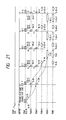
- Fig. 24 shows a procedure in the embodiment and images which are obtained by the embodiment.
- the CPU 4360 of the image memory apparatus 3 read out the input SV video images in accordance with the order registered in the SV jacket (S01), reduces (S02), and stores into the FIFO memories 4050R, 4050G, and 4050B.
- the image data is reduced in the main scanning direction by setting the data in the RAM 4212 in the image effective area into "1" in accordance with the reduction ratio.
- the data transfer from the FIFO memories 4050R, 4050G, and 4050B shown in Fig. 12 to the memories 4060R, 4060G, and 4060B shown in Fig. 15 is executed in a manner similar to the case of the data writing control from the color reader 1 to the memories 4060R, 4060G, and 4060B in the above embodiment.
- the image data in the subscanning direction is reduced by setting the data into the RAM 4212 in Fig. 15 in a manner similar to the above.
- the video image data in the memories 4060R, 4060G, and 4060B of the reduced one SV image are transferred to display memories 4410R, 4410G, and 4410B shown in Fig. 10A, they are laid out from the upper left position in accordance with the order, and the input and reduction of the SV images and the arrangement into the display memories are repetitively executed for all of the SV images (S03).
- the video image data in which all of the images in the SV jacket were laid out on a single surface and which were stored in the display memories 4410R, 4410G, and 4410B pass through LUT 4420R, 4420G, and 4420B and are sent to D/A converters 4430R, 4430G, and 4430B.
- the video image data are converted into an analog R signal 4590R, an analog G signal 4590G, and an analog B signal 4590B synchronously with an SYNC signal 4590S from a display controller 4440 by the D/A converters 4430R, 4430G, and 4430B. These analog signals are output to the monitor.
- the display controller 4440 outputs an SYNC signal 9600 synchronously with output timings of those analog signals.
- index image surface The images (hereinafter, referred to as index image surface) in which all of the image data in the SV jacket were reduced and laid out in one image surface are displayed on the monitor 32.
- the control unit 13 displays the index Nos. in the SV jacket corresponding to the SV index image surface onto the liquid crystal touch panel of the operation unit 20 (S05).
- the operator presses the index No. portion displayed on the touch panel.
- the control unit 13 discriminates the index No. of the designated SV and stores the index No. into the storage area in the control unit 13 (S06).
- the display of the touch panel of the operation unit 20 is switched to the display of the frame of the paper image which has previously been stored in the control unit 13 and the display of a plurality of frames of a fixed layout in the paper image frame (S07).
- the operator selects a desired layout position in the paper where the image of the selected SV index No. is arranged from a plurality of frames displayed and designates it by pressing the touch panel at that position.
- the control unit 13 stores the information in which the selected SV index No. and the position information in the paper of the image output are made correspond into the storage area in the control unit 13, that is, into an RAM 1013 shown in Fig. 1 (S08).
- step S09 the processing routine advances from step S09 to step S10.
- the image data of the equal size are read out from the SV jacket in accordance with the order of the index Nos. stored in the storage area in the control unit 13 without executing the reduction (S10).
- the capacity of the image surface is set to 640 pixles (H) x 480 pixels (V).
- the CPU 4360 of the image memory apparatus 3 first writes the "0" data into the RAM 4212 by the amount of 640 pixels in the main scanning direction.
- the input of the selector 4213 is switched to the counter 4214 side.
- the data from the RAM 4212 is set to the data for the WE signal control of the FIFO memories 4050R, 4050G, and 4050B.
- the data of one main scanning operation of the video images in the memories 9060R, 9060G, and 9060B as output signals from the A/D converters 4020R, 4020G, and 4020B are stored into the FIFO memories 4050R, 4050G, and 4050B at the equal size.
- the image data are transferred from the FIFO memories 4050R, 4050G, and 4050B to the memories 4060R, 4060G, and 4060B, the above operation is executed for all of the SV images selected in step S08, and a plurality of SV images are stored into the image memories 4060R, 4060G, and 4060B.
- the images are laid out on the basis of the position and size data stored in the control unit 13 and are output and printed by the color printer 2 (S11).
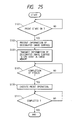
- steps S10 and S11 will now be further described in detail with reference to Figs. 25 and 26.
- the SV record regenerating apparatus 31 executes the operation in accordance with commands which are input from the CPU 4360 in the image memory apparatus 3 through a GPIB controller 4310.
- the CPU 4360 in the image memory apparatus 3 executes the communication with the control unit in the color reader 1 and the operation is controlled.
- Fig. 25 is a flowchart for the operation of the control unit in the color reader 1.
- Fig. 26 is a flowchart for the operation of the CPU 4360 in the image memory apparatus 3.
- the index Nos. that is, the information of the designated image surface and the layout data which were selected and designated in steps S05 to S09 are read out of the RAM 1013 in the color reader 1 (S103).
- the designated image surface data and the layout data are transmitted to the CPU 4360 in the image memory apparatus 3 via the CPU bus (S105).
- the image memory apparatus 3 Upon reception of the transmitted data, the image memory apparatus 3 again executes the regenerating operation and the storing operation of the image signals from the SV record regenerating apparatus as will be explained hereinlater.
- step S107 If a freeze completion signal is obtained from the SV record regenerating apparatus 31 (S107), the processing routine advances to step S109. An instruction to allow the printer 2 to execute the printing operation is given (S109). The system waits for completion of the printing operation (S111) and the processing routine is finished.
- the CPU 4360 in the image memory apparatus 3 receives the designated image surface data and the layout data from the control unit (S201). The CPU 4360 then gives an instruction for regeneration to the SV record regenerating apparatus 31 so as to regenerate the designated image surface (S203).
- the image data of the equal size are written into the memories 4060R, 4060G, and 4060B in a manner as mentioned above (S205).
- a check is made to see if the image data to be stored next exists or not on the basis of the designated image surface data and the layout data mentioned above (S207). If the data to be stored next does not exist, the freeze completion signal is transmitted to the color reader 1 (S209).
- freeze completion signal has been transmitted, a check is made to see if the ITOP signal has been input from the printer 2 or not (S211).
- the image data stored in the memories 4060R, 4060G, and 4060B are read out synchronously with the detected STOP signal (S213).
- the invention is not limited to such an apparatus.
- the invention can be also applied to other image sources such as VTA, image files, and the like.
- only the necessary image data can be efficiently selected from the memory apparatus to store the image data and images can be formed on the image forming medium.
Abstract
Description
- The present invention relates to an image processing system and, more particularly, to a processing system for regenerating image data from a medium in which the image data has been stored and forming an image.
- Recently, a digital television, a video printer, and the like have been proposed as apparatuses in which input color information is once stored into memory means such as a semiconductor memory or the like and, thereafter, the stored image data is read out and an image is formed, and the image is displayed, printed, or the like.
- However, in those apparatuses, a video signal for television is merely output, and a size of image source of the video signal and the size and output position of the image source of the video signal to an output medium for outputting are also unconditionally determined. One of the input image data is merely displayed and output or is printed as a hard copy at a predetermined size and at a predetermined position and its function is limited.
- In recent years, the signal which is displayed or output to an image processing apparatus such as a television receiver or the like is not limited to the video signals of those apparatuses but an image from an SV record regenerating apparatus or the like or from a personal computer, a work station, a color scanner, or the like also needs to be output to the image processing apparatus.
- However, the image stored in the SV record regenerating apparatus, a computer, or the like comprises a plurality of image data. There is a drawback such that it is impossible to easily select desired one of those plurality of image data and to layout and output the selected image data to an arbitrary or fixed position on an output paper.
- It is an object of the present invention to provide an image processing system which can easily select desired image data from a plurality of image data stored and can, further, form an image at an arbitrary position in consideration of the above problems.
- In addition to the above object, it is another object of the invention to provide an image processing system which can form an image of a high quality.
- Still another object of the invention is to provide an image processing system which is suitable to select and regenerate a color image.
- To accomplish the above objects, according to an embodiment of the invention, there is provided an image forming apparatus for receiving image data from a memory apparatus to store image data and forming an image onto an image forming medium, wherein the apparatus comprises: means for reducing the image data stored in the image memory apparatus; means which can display a plurality of images onto a display image surface by the reducing means and can select a plurality of arbitrary images from the plurality of images displayed; and image forming means for forming images of the image data which were selected by the selecting means and designated in the image memory apparatus to desired positions on the image forming medium.
- The above and other objects and features of the present invention will become apparent from the following detailed description and the appended claims with reference to the accompanying drawings.
-
- Fig. 1 is a system constructional diagram of an embodiment according to the present invention;
- Fig. 2 is a detailed block diagram of a
color reader 1 of the embodment; - Figs. 3 to 6 are diagrams schematically showing examples of the switching control of a video interface unit of the
color reader 1 of the embodiment; - Fig. 7 is an external view of a digitizer of the embodiment;
- Fig. 8 is a diagram for explaining address data indicated by the digitizer of the embodiment;
- Fig. 9 is an output timing chart from an interface unit to an image memory apparatus of the embodiment;
- Figs. 10A and 10B are detailed block diagrams of the image memory apparatus of the embodiment;
- Fig. 11 is a detailed diagram of a selector unit of the image memory apparatus of the embodiment;
- Fig. 12 is a detailed diagram of a system controller unit and an FIFO memory of the image memory apparatus of the embodiment;
- Fig. 13 is a timing chart for data storage from the system controller unit to the FIFO memory in the equal size mode of the embodiment;
- Fig. 14 is a timing chart for data storage from the system controller unit to the FIFO memory in the variable magnification mode of the embodiment;
- Fig. 15 is a detailed diagram of a construction of the system controller unit and image memories of the image memory apparatus of the embodiment;
- Fig. 16 is an arrangement diagram of image data in image memories of the image memory apparatus of the embodiment;
- Fig. 17 is a diagram showing an image formation layout of the embodiment;
- Fig. 18 is a timing chart for the image forming process according to the image formation layout of Fig. 17;
- Fig. 19 is an arrangement diagram of image data in memories of another image memory apparatus of the embodiment;
- Fig. 20 is a diagram showing an arbitrary layout state of the image data shown in Fig. 19;
- Fig. 21 is a timing chart upon image formation at line "ℓ₁" shown in Fig. 20;
- Fig. 22 is a timing chart upon image formation at line "ℓ₂" in Fig. 20;
- Fig. 23 is a timing chart for the image forming process of the embodiment;
- Fig. 24 is a flowchart showing an example of an operation procedure of the embodiment; and
- Figs. 25 and 26 are flowcharts for explaining the operations of a
color reader 1 and animage memory apparatus 3, respectively. - An embodiment of the present invention will be described in detail hereinbelow with reference to the drawings.
- Fig. 1 is a system constructional diagram showing an example of a schematic internal construction of a color image forming system of an embodiment according to the invention. As shown in Fig. 1, the system of the embodiment comprises: a digital color image reading apparatus (hereinafter, referred to as a "color reader") 1 to read a digital color image which is arranged in the upper portion of the system; and a digital color image printing apparatus (hereinafter, referred to as a "color printer") 2 to print and output a digital color image, an
image memory apparatus 3, an SVrecord regenerating apparatus 31, amonitor television 32, and ahost computer 33 which are arranged in the lower portion of the system. - The
color reader 1 of the embodiment comprises color separating means, which will be explained hereinlater, and a photoelectric converting device which is constructed by a CCD or the like. Thecolor reader 1 reads color image data of a read original every color and converts into electric digital image signals. - On the other hand, the
color printer 2 is a laser beam color printer of the electrophotographic type in which color images are limited every color in accordance with the digital image signal to be output and are copy transferred onto a recording paper a plurality of times in a digital dot form and recorded. - The
image memory apparatus 3 is an apparatus in which a read digital image from thecolor reader 1 is stored or an analog video signal from the SVrecord regenerating apparatus 31 is digitized and converted into a digital image and, thereafter, the digital image is stored. - The SV
record regenerating apparatus 31 is an apparatus in which images are photographed by an SV camera and the image data recorded in a SV floppy is regenerated and output as an analog video signal. On the other hand, the SVrecord regenerating apparatus 31 can receive an analog video signal and can also record into an SV floppy in addition to the above functions. - The
monitor television 32 displays images stored in theimage memory apparatus 3 and also displays the content of the analog video signal output from the SVrecord regenerating apparatus 31. - The
host computer 33 has functions to transmit the image data to theimage memory apparatus 3 and to receive the image data from thecolor reader 1 or the SV record regenerating apparatus which has been stored in theimage memory apparatus 3. Thehost computer 33 also controls thecolor reader 1 andcolor printer 2 and the like. - Each of the above sections will now be described in detail hereinbelow.
- A construction of the
color reader 1 will be first described. - In the
color reader 1 in Fig. 1,reference numeral 999 denotes an original; 4 indicates a platen glass onto which an original is put; and 5 represents a rod array lens for converging a reflected light image from the original which was exposed and scanned by ahalogen exposure lamp 10 and for inputting the image into an equal size typefull color sensor 6. Therod array lens 5, thefull color sensor 6, a sensor outputsignal amplifying circuit 7, and thehalogen exposure lamp 10 integrally construct anoriginal scanning unit 11. Thescanning unit 11 exposes and scans the original 999 in the direction indicated by an arrow (A₁). The image data of the original 999 to be read is sequentially read every line by exposing and scanning theoriginal scanning unit 11. The read color separation image signal is amplified to a predetermined voltage by the sensor outputsignal amplifying circuit 7. Thereafter, it is input to a video processing unit via asignal line 501 and processed. Thesignal line 501 is constructed as a coaxial cable to guarantee the signal transmission with a high fidelity.Reference numeral 502 denotes a signal line to supply drive pulses of the equal size typefull color sensor 6. All of the necessary drive pulses are produced in avideo processing unit 12.Reference numerals white plate 8 and theblack plate 9 by thehalogen exposure lamp 10, respectively, and are used to correct the white and black levels of the video signal. -
Reference numeral 13 denotes a control unit to control thewhole color reader 1 of the embodiment having a microcomputer. Thecontrol unit 13 executes the display on anoperation panel 20, the control of key inputs, the control of thevideo processing unit 12, and the like through abus 508. In addition, thecontrol unit 13 detects the position of theoriginal scanning unit 11 through signal lines 509 and 510 on the basis of detection signals by position sensors S₁ and S₂. - Further, the
control unit 13 executes all of the controls in thecolor reader 1. That is, thecontrol unit 13 controls a steppingmotor drive circuit 15 to pulse drive a steppingmotor 14 to move thescanning unit 11 through asignal line 503. Thecontrol unit 13 controls the on/off operations and a light amount of thehalogen exposure lamp 10 by anexposure lamp driver 21 through asignal line 504. Thecontrol unit 13 controls adigitizer 16, internal keys, the display section, and the like through asignal line 505. - The color image signal which was read by the
exposure scanning unit 11 upon exposing and scanning of the original is input to thevideo processing unit 12 through the sensor outputsignal amplifying circuit 7 and thesignal line 501. - The
original scanning unit 11 andvideo processing unit 12 will now be described in detail with reference to Fig. 2. - The color image signal input to the
video processing unit 12 is separated into three color signals of G (green), B (blue), and R (red) by a sample and hold circuit S/H 43. The separated color image signals are analog processed by an analog colorsignal processing circuit 44 and, thereafter, they are A/D converted into the digital color image signals. - In the embodiment, the
color reading sensor 6 in theoriginal scanning unit 11 is constructed in a zigzag shape which is divided into five areas as also shown in Fig. 2. Deviations of the reading positions among thechannels channels color reading sensor 6 and anFIFO memory 46. The signals after the positional deviations were corrected which are output from theFIFO memory 46 are input to a black correction/white correction circuit 85. A variation in the dark state of thesensor 6, a variation in light amount of thelamp 10, a variation in sensitivity of the sensor, and the like are corrected by using the signals corresponding to the reflected lights from thewhite plate 8 andblack plate 9 mentioned above. - The color image data which is proportional to the input light amount of the
color sensor 6 is input to avideo interface 101 and connected to theimage memory apparatus 3. - The
video interface 101 has the following four functions as shown in Figs. 3 to 6: that is, - (1) the function to output a
signal 559 from the black correction/white correction circuit 85 to the image memory apparatus 3 (Fig. 3), - (2) the function to input the image data from the
image memory apparatus 3 to a logarithm conversion circuit 86 (Fig. 4), - (3) the function to output the image data from a
printer interface 56 to the image memory apparatus 3 (Fig. 5), and - (4) the function to transmit the
signal 559 from the black correction/white correction circuit 85 to the logarithm conversion circuit 86 (Fig. 6). - The above four functions are switched as shown in Figs. 3 to 6 by the
CPU control line 508. - The reading (fetching) control in the
color reader 1 and the storage control of the read image data into theimage memory apparatus 3 in the embodiment will now be described. - The reading operation by the
color reader 1 is executed by a digitizer, which will be explained hereinafter. Fig. 7 shows an external view of thedigitizer 16. - In Fig. 7,
reference numeral 427 denotes an entry key to transfer the image data from thecolor reader 1 to theimage memory apparatus 3. A coordinate detectingplate 420 is used to set an arbitrary area on the reading original or to set a reading magnification or the like. Apoint pen 421 is used to designate the coordinates of the pen. - To transfer the image data of an arbitrary area on the original to the
image memory apparatus 3, theentry key 427 in Fig. 7 is depressed and, thereafter, a reading position is indicated by thepoint pen 421. - The image data of the reading area is sent to the
video processing unit 12 through thecommunication line 505 in Fig. 1. Thevideo processing unit 12 transmits the input image signal from thevideo interface 101 to theimage memory apparatus 3 by theCPU control line 508. - After the
entry key 427 in Fig. 7 was depressed, if a reading position is not indicated by thepoint pen 421, thecolor reader 1 detects a size of original 999 by the prescan and transmits the size data as image reading area information to theimage memory apparatus 3 through thevideo interface 101. - A process to transmit the information of the indicated area of the original 999 to the
image memory apparatus 3 will now be described. - Fig. 8 shows an example of addresses of the information (points A and B) of the area indicated by the
point pen 421 of thedigitizer 16. - The
video interface 101 outputs not only the area information but also a VCLK signal, anITOP signal 551, anEN signal 104 as a signal from an areasignal generation circuit 51, and the like to theimage memory apparatus 3 together with the image data. Fig. 9 shows a timing chart for those output signal lines. - As shown in Fig. 9, by pressing a start button of the
operation unit 20, the steppingmotor 14 is driven and theoriginal scanning unit 11 starts the scanning. When thescanning unit 11 reaches the front edge of the original, theITOP signal 551 is set to the "1" level. Thescanning unit 11 reaches the area designated by thedigitizer 16. During the scanning of the designated area, theEN signal 104 is held at the "1" level. Therefore, it is sufficient to input the read color image data (DATA EN signal 104 is set to "1". - As shown in Fig. 9 mentioned above, in the transfer of the image data from the
color reader 1, by controlling thevideo interface 101 in a manner as shown in Fig. 3, theR data 105,G data 106, andB data 107 are transmitted to theimage memory apparatus 3 in a real-time manner synchronously with theITOP signal 551, control signal of theEN signal 104, and VCLK signal. - A practical method of storing by the
image memory apparatus 3 on the basis of the image data and the control signal will now be described with reference to Figs. 10A and 10B. - A
connector 4550 is connected to thevideo interface 101 of thecolor reader 1 through a cable. TheR data 105,G data 106, andB data 107 are connected to aselector 4250 throughsignal lines EN signal 104, and ITOP signal 551 which are sent from thevideo interface 101 pass through asignal line 9450 and are directly input to asystem controller 4210. On the other hand, prior to reading the original, the area information designated by thedigitizer 16 passes through acommunication line 9460 and is input to areader controller 4270. The area information is output from thereader controller 4270 to aCPU 4360 through aCPU bus 9610. TheR data 105,G data 106, andB data 107 which were input to theselector 4250 through thesignal lines selector 4250 and, thereafter, they are output to signallines FIFO memories - Fig. 11 shows a detailed constructional diagram of the
selector 4250. - As shown in the diagram, in the case of storing the image data from the
color reader 1 to theimage memory apparatus 3, a control signal SELECT-A 9451A from thesystem controller 4210 is set to 1, a control signal SELECT-B 9451B is set to 1, and a control signal SELECT-C 9451C is set to 0. Only tristate buffers 4251E, 4251V, 4251R, 4251G, and 4215B are made operative and other tristate buffers 4255E, 4255V, 4255R, 4255G, 4255B, 4256E, 4256V, 4256R, 4256G, and 4256B are set to the high impedance, respectively. - Similarly, the VCLK signal and
EN signal in thecontrol signal 9450 are also selected by the SELECT signals 9451A, 9451B, and 9451C. In the case of storing the image data from thecolor reader 1 into theimage memory apparatus 3, as shown in Fig. 11, the VCLK signal andEN signal are the signals which are output from thecolor reader 1. Only the tristate buffers 4251E and 4251V are made operative. Thus, those signals pass through signal lines CLKIN 9456 andENIN 9457 and are input to thesystem controller 4210. - On the other hand, control signals
VSYNCIN HSYNCIN connector 4550 to thesystem controller 4210. - Further, the
selector 4250 also has the function to average the image data from thecolor reader 1. Thesignals - Outputs from the FIFO memories 4252R, 4252G, and 4252B are the signals which are delayed by one main scanning period than the image data 9421R, 9421G, and 9421B and pass through signal lines 9422R, 9422G, and 9422B and are input to adders 4253R, 4253G, and 4253B. The signals 9421R, 9421G, and 9421B from the tristate buffers 4251R, 4251G, and 4251B are input to the adders 4253R, 4253G, and 4253B. The adders 4253R, 4253G, and 4253B each calculate the mean value of total four pixels comprising two pixels in the main scanning direction and two pixels in the subscanning direction and output to signal lines 9423R, 9423G, and 9423B.
- Selectors 4254R, 4254G, and 4254B select either the image signals 9421R, 9421G, and 9421B from the
color reader 1 or the weighted mean signals 9423R, 9423G, and 9423B and output thesignals FIFO memories - The
system controller 4210 transfers only the effective area of the image among theimage data FIFO memories system controller 4210 also simultaneously executes the trimming process and the variable magnifying process. - Further, the
FIFO memories color reader 1 and theimage memory apparatus 3. - The above processes in the embodiment will now be described hereinbelow with reference to a circuit diagram of Fig. 12 and a timing chart of Fig. 13.
- That is, before the data are transferred from the selectors 4254R, 4254G, and 4254B into the
FIFO memories digitizer 16 is written intocomparators CPU bus 9610. - A start address in the main scanning direction of the area designated by the
digitizer 16 is set into thecomparator 4232, while a stop address is set into thecomparator 4233. - On the other hand, in the subscanning direction of the area designated by the
digitizer 16, theCPU bus 9610 side is selected and is made effective by controlling aselector 4213. The "0" data is written into the effective area of the area designated in anRAM 4212, while the "1" data is written into the ineffective area. - In the variable magnifying process in the main scanning direction, a variable magnification ratio is set into a
rate multiplier 4234 through theCPU bus 9610. The variable magnifying process in the subscanning direction can be realized by the data which is written into theRAM 4212. - Fig. 13 is a timing chart in the case of executing the trimming process. As mentioned above, in the case of storing only the area designated by the
digitizer 16 into the memory (trimming process), the trimming position in the main scanning direction is set into thecomparators RAM 4212 by the CPU by switching theselector 4213 to the side of the CPU bus 9610 ((for instance) trimming area:main scan 1000 to 3047; subscan 1000 to 5095). - For a trimming
interval signal 9100 in the main scanning direction, when acounter 4230 operates synchronously with theHSYNCIN signal 9452 andCLKIN signal 9456 and acounter output 9103 is set to 1000, the output of thecomparator 4232 is set to 1 and a Q output of a flip-flop 4235 is set to 1. Subsequently, when thecounter output 9103 is set to 3047, the output of thecomparator 4233 is set to 1 and the output of the flip-flop 4235 is set from 1 to 0. On the other hand, in the timing chart of Fig. 13, since the equal size magnifying process is executed, an output of therate multiplier 4234 is set to 1. The image data inaddresses 1000 to 3047 in the color image data which is input into theFIFO memories interval signal 9100 is written into theFIFO memories - On the other hand, a
comparator 4231 outputs a signal 9102 which is delayed by pixels than theHSYNCIN signal 9452. As mentioned above, the providing the phase difference between the signals which are input toRSTW andRSTR input terminals of each of theFIFO memories CLKIN signal 9456 and theCLK signal 9453 which are input to theFIFO memories - For the trimming in the subscanning direction, a
counter 4214 side is first selected and is made effective by controlling theselector 4213 and aninterval signal 9104 synchronized with theVSYNCIN signal 9455 andHSYNCIN signal 9452 is output from theRAM 4212. Theinterval signal 9104 is synchronized with the signal 9102 by a flip-flop 4211 and is input to a reset read (RE ) input terminal of each of theFIFO memories FIFO memories trimming signal 9101 is set to "0". - Although only the trimming process has been described above, the variable magnifying process can be also executed simultaneously with the trimming. To execute the variable magnifying process in the main scanning direction, a variable magnification ratio is set into the
rate multiplier 4234 through theCPU bus 9610. On the other hand, the variable magnifying process in the subscanning direction can be realized on the basis of the data which is written into theRAM 4212. - Fig. 14 shows a timing chart in the case where the trimming process and the variable magnifying process (50%) were executed.
- Fig. 14 is a diagram showing an example of the timing chart in the case where the image data from the selectors 4254R, 4254G, and 4254B are reduced by 50% by executing the variable magnifying process and the reduced image data are transferred to the
FIFO memories - The variable magnification ratio of 50% reduction is set into the
rate multiplier 4234 in Fig. 12 through theCPU bus 9610. At this time, anoutput 9106 of therate multiplier 4234 has a waveform such that "0" and "1" are repeated every pixel in the main scanning direction as shown in Fig. 14. The ANDsignal 9100 of theoutput signal 9106 of therate multiplier 4234 and aninterval signal 9105 formed by thecomparators FIFO memories - On the other hand, for the variable magnifying process in the subscanning direction, as shown in Fig. 14, by setting the write data (read enable signal to the
FIFO memories RAM 4212 into "1" (inhibition of the reading operation) in the image data effective area, only the image data which was reduced by 50% is sent to imagememories signal 9101 is alternately repetitively set to the "1" and "0" data, thereby executing the reduction of 50%. - That is, in the trimming process and variable magnifying process in the main scanning direction, the write enable operations of the
FIFO memories FIFO memories - The image data transfer from the
FIFO memories memories control line 9101. - The
control line 9101 corresponds to the read enable signal of theFIFO memories memories - When the
control line 9101 is set to "0", the image data which was read out of theFIFO memories tristate buffers memories CLK signal 9453 and passes through a selector 4070 and is input to anADR 9110 of each of thememories - At this time, since the write enable
WE signal 9101 of thememories image data memories - In the embodiment, the memory capacity of each color is set to 1 Mbytes. Therefore, by reducing the image data of the read area in Fig. 8 by 50%, the read image data is converted into the data of the maximum capacity of each memory provided in the
image memory apparatus 3 and is stored. - On the other hand, in the above embodiment, the
CPU 4360 calculates the effective area from the information of the area of the original of the A3 size which was designated by thedigitizer 16. TheCPU 4360 then sets the data corresponding to thecomparators 4231 to 4233,rate multiplier 4234, andRAM 4212. - In the embodiment, since the capacity of the read image data is larger than the capacity of the image memory provided in the apparatus, the reducing process is executed and the image data is converted into the small data of the capacity which can be stored and, thereafter, it is stored into the image memory. However, if the capacity of the read image data is smaller than the image memory capacity, by setting a CLR signal 9171 in Fig. 15 to "1", a plurality of image surfaces can be simultaneously stored into the image memory. In this case, the trimming data is set into the
comparators digitizer 16 to the memory and the equal size mode is set into therate multiplier 4234. On the other hand, as the write data to theRAM 4212, all of the image effective areas are set to "0" and the other areas are set to "1" and the equal size is set. - In order to store the read image data into the memory while keeping the aspect ratio (the ratio of the vertical size to the horizontal size) of the read image, the
CPU 4360 first obtains the number "x" of effective pixels from the area data sent from thedigitizer 16. Then, the CPU obtains a reduction ratio "z" from the maximum capacity "y" of the image memory by the following equation.

Thus, - (1) when
z 100 ≧ 100, 100% is set into therate multiplier 4234, all of the effective image areas in theRAM 4212 are set to "0", and the image data is stored in the equal size mode, and - (2) when z < 100, z% of the reduction is set into the
rate multiplier 4234, the image data in theRAM 4212 is reduced by z%, and the reduced image data is stored into the maximum capacity of the memory while keeping the aspect ratio. - In this case as well, as the data which is written into the
RAM 4212, it is sufficient to properly write the data of "1" and "0" in correspindence to the reduction ratio "z". - By controlling as mentioned above, an arbitrary variable magnifying process can be easily executed by merely controlling the inside of the
image memory apparatus 3 while keeping the aspect ratio of the input image. The read image can be effectively recognized. Further, the using efficiency of the memory capacity can be set to the maximum value. - As shown in Fig. 1, the system of the embodiment can not only store the video image from the SV
record regenerating apparatus 31 into theimage memory apparatus 3 but also output to themonitor television 32 or thecolor printer 2. Theimage processing apparatus 3 also executes the handling of the input image. - Inputting of the video image from the SV
record regenerating apparatus 31 to theimage memory apparatus 3 will now be described hereinbelow. - First, the inputting control of the video image from the SV
record regenerating apparatus 31 to theimage memory apparatus 3 will be first described hereinbelow with reference to block constructional diagrams of theimage memory apparatus 3 of Figs. 10A and 10B. - The video image from the SV
record regenerating apparatus 31 is input in a form of an NTSCcomposite signal 9000 through ananalog interface 4500 and is separated into four signals 9015R, 9015G, 9015B, and 9015S (these signals are generally referred to as 9015) comprising separate R, G, B signals and a composite SYNC signal by adecoder 4000. - On the other hand, the
decoder 4000 also decodes Y (luminance)/C (chrominance) signals 9010 from ananalog interface 4510 in a manner similar to the above.Signals selector 4010 in a form of the separate R, G, and B signals and the composite SYNC signal. Aswitch 4530 is provided to control theselector 4010 for selecting and switching either the input signals 9020R, 9020G, 9020B, and 9020S or the signals 9015R, 9015G, 9015B, and 9015S. When theswitch 4530 is open, thesignals 9020R to 9020S are selected. When theswitch 4530 is closed, the signals 9015R to 9015S are selected. - Separate R, G, and
B signals selector 4010 are analog/digital converted into digital signals by A/D converters - On the other hand, a selected
composite SYNC signal 9050S is input to a TBC/HV separation circuit 4030. Aclock signal 9060C, ahorizontal sync signal 9060H, and avertical sync signal 9060V are produced from thecomposite SYNC signal 9050S by the TBC/HV separation circuit 4030. Those sync signals are supplied to thesystem controller 4210. - The
TVCLK signal 9060C which is output from the TBC/HV separation circuit 4030 in the embodiment is the clock signal of 12.25 MHz, theTVHSYNC signal 9060H is the signal of a pulse width of 63.5 µsec, and theTVVSYNC signal 9060V is the signal of a pulse with of 16.7 msec. - The
FIFO memories TVHSYNC signal 9060H and data 9060R, 9060G, and 9060B are written into the FIFO memories from address "0" synchronously with theTVCLK signal 9060C. At this time, the writing operations to theFIFO memories WE signal 9100 which is output from thesystem controller 4210 is set to "1". - The writing control of the
FIFO memories WE signal 9100 will be described in detail hereinbelow. - The SV
record regenerating apparatus 31 in the embodiment is based on the NTSC standard. Therefore, when the video image from the SVrecord regenerating apparatus 31 is digitized, the image surface capacity is set to 640 pixels (in the horizontal direction: H) x 480 pixels (in the vertical direction: V). Therefore, theCPU 4360 of theimage memory apparatus 3 first writes set values into thecomparators CPU 4360 switches the input signals of theselector 4213 to theCPU bus 9610 side and writes "0" data as many as 480 pixels in the subscanning direction into theRAM 4212. - On the other hand, the data of 100% is set into the
rate multiplier 4234 to set the magnification in the main scanning direction. - In the case of storing the image data from the SV
record regenerating apparatus 31 into thememories system controller 4210 connects theTVVSYNC signal 9060V,TVHSYNC signal 9060H, andTVCLK signal 9060V which are output from the TBC/HV separation circuit 4030 to theVSYNCIN signal 9455,HSYNCIN signal 9452, andCLKIN signal 9456 shown in Fig. 12. - As mentioned above, by setting the image control signal to the interface side of the SV record regenerating apparatus, the data of the single main scan of the video images of the output signals 9060R, 9060G, and 9060G from the A/
D converters FIFO memories - On the other hand, in the case of reducing the input SV video images and storing into the
FIFO memories rate multiplier 4234 and the data in theRAM 4212 in the image effective area is set to "1" in accordance with the reduction ratio, so that the video image can be reduced. - The data transfer from the
FIFO memories memories color reader 1 to thememories - On the other hand, the SV
record regenerating apparatus 31 in the embodiment is based on the NTSC standard. The case where the aspect ratio of the digital image in the main scanning direction to the subscanning direction is set to 4:3 has been described as an example. However, by rewriting the contents of thecomparators RAM 4212 in Fig. 12, the invention can be also applied to the aspect ratio of 16:9 of the HDTV standard which is presumed as the standard of the future television. - In addition, the memory capacity in the embodiment has been set to 2 Mbytes. However, since the capacity of one image surface of the NTSC standard is set to about 0.3 Mbytes, the images of six image surfaces can be stored. Such storage of six image surfaces can be also realized by setting the
CLR signal 9171 shown in Fig. 15 to "1". - In the case of the HDTV standard of 1840 pixels (in the main scanning direction) x 1035 pixels (in the subscanning direction), by setting the
CLR signal 9171 to "0", one image surface can be stored into the memory of 2 Mbytes. - Further, the invention can also cope with the realization of the high band of the video apparatuses. That is, by raising the TVCLK clocks which are output from the TBC/
HV separation circuit 4030 in the embodiment, the number of read pixels in the main scanning direction can be increased. - The reading process of the image data from the
memories image memory apparatus 3 described above will now be explained. - A command input and the like in the case where an image is formed by the
color printer 2 on the basis of the image outputs from the memories are mainly executed by thedigitizer 16 shown in Fig. 7 mentioned above. - In Fig. 7,
reference numeral 428 denotes an entry key for allowing thecolor printer 2 to form an image onto a recording paper in accordance with the size of recording paper on the basis of the image data from thememories Reference numeral 429 indicates an entry key for allowing an image to be formed at the position designated by the coordinate detectingplate 420 of thedigitizer 16 and by thepoint pen 421. - First, explanation will be made with respect to an embodiment in which an image is formed in accordacne with the size of recording paper. Then, an embodiment in which an image is formed in the area designated by the digitizer will be described.
- In the embodiment, as shown in Fig. 1, the
color printer 2 has twocassette trays operation unit 20. The following description relates to the case of forming a plurality of images onto the recording paper of the A4 size. - Prior to forming an image, by inputting the read image data from the
color reader 1 mentioned above to theimage memory apparatus 3, total sixteen image data comprising "image 0" to "image 15" are read out of thecolor reader 1 and are stored into theimage memories - Next, the
entry key 428 of thedigitizer 16 is pressed. Thus, the CPU (not shown) detects such a key input and automatically sets the image forming position to the recording paper of the A4 size. In the case of forming the image of No. 16 shown in Fig. 16, for instance, the image forming position is set as shown in Fig. 17. - The above image forming process in the embodiment will now be described in detail hereinbelow with reference to the block diagrams of Figs. 10A and 10B and a timing chart shown in Fig. 18.
- An ITOP signal 511 which is sent from the
color printer 2 shown in Fig. 2 to thecolor reader 1 through theprinter interface 56 is input to thevideo interface 101 in thevideo processing unit 12. The ITOP signal is then sent from thevideo interface 101 to theimage memory apparatus 3. Theimage memory apparatus 3 starts the image forming process in response to theITOP signal 551. Each image sent to theimage memory apparatus 3 is formed under the control of thesystem controller 4210 shown in Figs. 10A and 10B in theimage memory apparatus 3. - In Figs. 10A and 10B, an output of the counter 0 (4080-0) is selected by the selector 4070. The
memories memory address line 9110. Due to the access, the image data stored in thememories Conversion data UCR circuit 4120. The color correction of the color image signals in theimage memory apparatus 3 is executed by the masking/black extraction/UCR circuit 4120 and the UCR/black extraction processes are also executed in the black recording mode. - A
sequential image signal 9210 from the masking/black extraction/UCR circuit 4120 is separated every image by aselector 4130. The separated signals are input to FIFO memories 4140-0 to 4140-3. The images which have sequentially been arranged so far can be processed in parallel by the functions of the FIFO memories 4140-0 to 4140-3. - The relations among the readout image signals 9160R, 9160G, and 9160B from the memories and parallel output image data 9260-0 to 9260-3 from the FIFO memories are shown in the upper stage portion in Fig. 18. As shown in the diagram, the image data 9260-0 to 9260-3 corresponding to the readout image data at the line "0" of "
image 0" to "image 3" which are necessary to form an image of one line in the main scanning direction can be all processed in parallel. - The parallel image signals 9260-0 to 9260-3 are input to enlargement/interpolation circuits 4150-0 to 4150-3 at the next stage. The circuits 4150-0 to 4150-3 are controlled by the
system controller 4210 so as to obtain a layout of the images shown in Fig. 17 and execute the enlargement/interpolation processes as shown by signals 9300-0 to 9300-3 in Fig. 18. In the embodiment, the primary interpolating method is used. - The interpolated signals 9300-0 to 9300-3 are input to a
selector 4190. The image data which were processed in parallel so far are again converted into the serial image data signal. Animage signal 9330 converted into the serial image data by theselector 4190 is subjected to an edge emphasizing process and a smoothing process by anedge filter circuit 4180. The processed image signal passes through anLUT 4200 and is input to theselector 4250 through asignal line 9380. - The signals input to the
selector 4250 pass through the tristate buffers 4256R, 4256G, 4256B, 4255R, 4255G, and 4255B and are output to theconnector 4550 through thesignal lines - Similarly, an
ENOUT signal 9454 and theCLK signal 9453 which are output from thesystem controller 4210 also pass through the tristate buffers 4256E, 4256V, 4255E, and 4255V and are output to theconnector 4550 through thesignal line 9450. - At this time, the control lines SELECT-A 9451A, SELECT-B 9451-B, and SELECT-C 9451-C to control the gates of the tristate buffers shown in Fig. 11 are set to "0", "0" and "1", respectively.
- After completion of the formation of all of the image data of "
image 0" to "image 3", the images are then sequentially formed in accordance with the order of "image 4" to "image 7", "image 8" to "image 11", and "image 12" to "image 15". In this manner, sixteen images of "image 0" to "image 15" shown in Fig. 17 are formed. - Although the control in which the images are developed so that they can be automatically formed as shown in Fig. 17 and the images are formed has been described above, the embodiment is not limited to the above example but images can be also formed by developing arbitrary images to arbitrary positions.
- An example of such a case will now be described hereinbelow with respect to the case where "
image 0" to "image 3" shown in Fig. 20 are developed as shown in the diagram and the images are formed. - First, four image data which were read out from the
color reader 1 are stored into theimage memories entry key 429 of thedigitizer 16, the system waits for the input of the designated image forming positions of the images read out from thedigitizer 16. - BY operating the
point pen 421, desired developing positions are designated and input by the coordinate detectingplate 420. For instance, the developing areas are designated and input as shown in Fig. 20. - The image forming process in this case will now be described hereinbelow with reference to block constructional diagrams of Figs. 10A and 10B and timing charts shown in Figs. 21 and 22.
- Fig. 21 is a timing chart in the case of forming the image at line "ℓ₁" shown in Fig. 20. Fig. 22 is a timing chart in the case of forming the image at line "ℓ₂" in Fig. 20.
- The ITOP signal 551 is output from the
color printer 2 in a manner similar to the above and thesystem controller 4210 starts the operation synchronously with the signal. - In the layout of the images shown in Fig. 20, "
image 3" is obtained by rotating the image from thecolor reader 1 by 90°. - The image rotating process is executed in the following procedure. First, the images are transferred from the
memories work memory 4390 by a DMAC (direct memory access controller) 4380 in Figs. 10A and 10B. Next, after the well-known image rotating process was executed in thework memory 4390 by theCPU 4360, the images are transferred from thework memory 4390 to thememories DMAC 4380, so that the image rotating process is executed. - The position data of the images which were laid out and indicated and input by the
digitizer 16 are sent to theimage memory apparatus 3 through thevideo processing unit 12 in Fig. 1. When thesystem controller 4210 receives the developing position data for the images, the system controller generates operation permission signals 9320-0 to 9320-3 of the enlargement/interpolation circuits 4150-0 to 4150-3 corresponding to the images. - In the layout of arbitrary positions in the embodiment, for instance, the counter 0 (4080-0) operates in correspondence to "
image 0" a counter 1 (4080-1) operates in correspondence to "image 1", a counter 2 (4080-2) operates in correspondence to "image 2", and a counter 3 (4080-3) operates in correspondence to "image 3", respectively. - Control upon image formation at line "ℓ₁" shown in Fig. 20 will now be described with reference to Fig. 21.
- When "
image 0" is read out of theimage memories image 0" shown in Fig. 19) are read out by the counter 0 (4080-0). The outputs of the counters 4080-0 to 4080-3 are switched by the selector 4070. - Similarly, in the case of reading out "
image 1", the image data from addresses "0.5M" to "1M" (storage area of "image 1" shown in Fig. 19) are read out by the counter 1 (4080-1). The reading timings are shown by 9160R, 9160G, and 9160B in Fig. 21. - The counters 4080-2 and 4080-3 are not operative by counter enable signals 9130-2 and 9130-3 from the
system controller 4210. - The image data of "
image 0" and "image 1" are sent to the masking/black extraction/UCR circuit 4120 through theLUT sequential color signal 9210. The areasequential color signal 9210 is converted into the parallel signals by theselector 4130 and separated every pixel and sent to the FIFO memories 4140-0 and 4140-1. When the operation permission signals 9320-0 and 9320-1 from thesystem controller 4210 to the enlargement/interpolation circuits 4150-0 and 4150-1 are set to the enable state, the circuits 4150-0 and 4150-1 set FIFO readout signals 9280-0 and 9280-1 to the enable state, thereby starting the reading control. - In response to the signals 9280-0 and 9280-1, the FIFO memories 4140-0 and 4140-1 start the transfer of the image data to the enlargement/interpolation circuits 4150-0 and 4150-1. The layout and interpolating calculations of the images are executed by the enlargement/interpolation circuits 4150-0 and 4150-1 in accordance with the area designated by the
digitizer 16. The timings for those operations are shown by 9300-0 and 9300-1 in Fig. 21. - After the image data of "
image 0" and "image 1" in which the layout and interpolating calculations had been executed were selected by theselector 4190, they pass through anedge filter circuit 4180 and are input to theLUT 4200. Since the processes until thesubsequent connector 4550 are similar to those mentioned above, their descriptions are omitted. - The timings for line "ℓ₂" shown in Fig. 20 will now be described with reference to Fig. 22.
- The processes from the
image memories - However, since both of the image data of "
image 1" and "image 2" have been output at line "ℓ₂", the counter 1 (4080-1), counter 2 (4080-2), FIFO memories 4140-1 and 4140-2, and enlargement/interpolation circuits 4150-1 and 4150-2 operate and they are controlled in accordance with the control signals from thesystem controller 4210. - As shown in Fig. 20, "
image 1" and "image 2" are overlapped at line "ℓ₂". In the overlap portion, a mode to form either one of the images or a mode to form both images can be selected by acontrol signal 9340 from thesystem controller 4210. - The practical control method is similar to that in the case mentioned above.
- Signals from the
connector 4550 are connected to thecolor reader 1 by the cable. Therefore, thevideo interface 101 of thecolor reader 1 selects and outputs theimage signal 105 from theimage memory apparatus 3 to theprinter interface 56 via the signal line path shown in Fig. 5. - The process to transfer the image data from the
image memory apparatus 3 to thecolor printer 2 in the image formation in the above embodiment will now be described in detail hereinbelow with reference to a timing chart of Fig. 23. - As mentioned above, by pressing the start button of the
operation unit 20, theprinter 2 starts operating and starts the conveyance of the recording paper. When the recording paper reaches the front edge of the image forming unit, theITOP signal 551 is output. The ITOP signal 551 is sent to theimage memory apparatus 3 through thecolor reader 1. Under the set conditions, theimage memory apparatus 3 reads out the image data stored in theimage memories video processing unit 12 of thecolor reader 1. Thevideo interface 101 of thevideo processing unit 12 changes the processing method in thevideo interface 101 in accordance with the kind (R, G, B)/(M, C, Y, Bk) of the data transmitted. - In the embodiment, since the area sequential image data of M, C, Y, and Bk is output, the above operations are repeated four times in accordance with the order of M, C, Y, and Bk, thereby forming an image.
- A construction of the
color printer 2 to print out the image signal processed by thevideo processing unit 12 as mentioned above will be described with reference to Fig. 1. - In the construction of the
printer 2 in Fig. 1,reference numeral 711 denotes a scanner having: a laser output unit to convert the image signal from thecolor reader 1 into the photo signal; a polygon mirror 712 of a polyhedron (for instance, octahedron); a motor (not shown) to rotate the polygon mirror 712; an f/ϑ lens (image forming lens) 713; and the like.Reference numeral 714 denotes a reflecting mirror to change the optical path of the laser beam from thescanner 711 shown by an alternate long and short dash line in the diagram, and 715 indicates a photo sensitive drum. - The laser beam emitted from the laser output unit is reflected by the polygon mirror 712 and scans (raster scan) like a line on the surface of the photo
sensitive drum 715 by the f/ϑ lens 713 and reflectingmirror 714, thereby forming an electrostatic latent image corresponding to the original image. -
Reference numeral 717 denotes a primary charging device; 718 indicates a whole surface exposure lamp; 723 a cleaner unit to collect the residual toner which was not copy transferred; and 724 a copy transfer precharging device. Those parts are arranged around the photosensitive drum 715.Reference numeral 726 denotes a developing unit to develop the electrostatic latent image formed on the surface of the photosensitive drum 715 by the laser exposure; 731Y (for yellow), 731M (for magenta), 731C (for cyan), and 731Bk (for black) indicate developing sleeves which are come into contact with the photosensitive drum 715 and directly execute the development; 730Y, 730M, 730C, and 730Bk toner hoppers to hold spare toners; and 732 a screw to transfer a developing agent. The developingunit 726 is constructed by the sleeves 731Y to 731Bk,toner hoppers 730Y to 730Bk, and screw 732. Those parts are arranged around a rotary shaft P of the developingunit 726. - For instance, when a yellow toner image is formed, the yellow toner development is executed at the position shown in the diagram. In the case of forming a magenta toner image, the developing
unit 726 is rotated around the shaft P as a rotational center in the diagram, thereby setting the developing sleeve 731M in the magenta developing unit to the position where the sleeve 731M is come into contact with the photosensitive drum 715. In the case of developing cyan and black images, the developingunit 726 is also rotated around the shaft P in the diagram as a rotational center and is made operative in a manner similar to the above. - On the other hand,
reference numeral 716 indicates a copy transfer drum to copy transfer the toner image formed on the photosensitive drum 715 onto the recording paper.Reference numeral 719 indicates an actuator plate to detect the moving position of thecopy transfer drum 716; 720 a position sensor to detect that thecopy transfer drum 716 has moved to the home position by approaching to theactuator plate 719; 725 a copy transfer drum cleaner; 727 a paper pressing roller; 728 a discharging device; and 729 a copy transfer charging device. Theabove parts copy transfer drum 716. - On the other hand,
reference numerals cassettes copy transfer drum 716. The process advances to the image forming step. - Reference numeral 550 denotes a drum rotating motor to synchronously rotate the photo
sensitive drum 715 and thecopy transfer drum 716; 750 indicates a peeling-off claw to peel off the paper from thecopy transfer drum 716 after completion of the image formation; 742 a conveying belt to convey the removed paper; and 743 an image fixing unit to fix the paper conveyed by thebelt 742. In theimage fixing unit 743, the rotating force of amotor 747 attached to amotor attaching section 748 is transferred through atransfer gear 746 to a pair ofthermal pressure rollers rollers - The printing-out process of the
printer 2 having the above construction will now be described hereinbelow with reference to the timing chart of Fig. 23 as well. - First, when the
first ITOP signal 551 is input, a Y latent image is formed onto the photosensitive drum 715 by the laser beam and is developed by the developing sleeve 731Y. The developed Y image is then copy transferred onto the paper on the copy transfer drum and the magenta printing process is executed. The developingunit 726 is then rotated around the shaft P in the diagram as a rotational center. - When the
next ITOP signal 551 is input, an M latent image is formed onto the photo sensitive drum by the laser beam and the cyan printing process is executed hereinafter by the similar operation. By also executing the above operation for the C and Bk latent images in response to the subsequent ITOP signals 551, the yellow and black printing processes are executed. After completion of the image formation, the recording paper is peeled off from the drum by the peeling-off claw 750 and the image is fixed by theimage fixing unit 743. In this manner, a series of color image printing processes are executed. - In the embodiment, the
video apparatus 1 is the SV recorder of the NTSC standard. A plurality of, for instance, fifty images are stored in a single SV jacket. In the case of outputting a single print, arbitrary number of images are selected from the stored SV images and an output layout of those images can be executed. Fig. 24 shows a procedure in the embodiment and images which are obtained by the embodiment. - First, all of the images registered in the SV jacket are reduced and images of a single surface which were laid out in accordance with the order (hereinafter, referred to as index Nos.) registered in the SV jacket are formed in accordance with the size which has previously been stored in an
ROM 4370 shown in Fig. 10B (steps S01 to S03). - That is, the
CPU 4360 of theimage memory apparatus 3 read out the input SV video images in accordance with the order registered in the SV jacket (S01), reduces (S02), and stores into theFIFO memories RAM 4212 in the image effective area into "1" in accordance with the reduction ratio. - The data transfer from the
FIFO memories memories color reader 1 to thememories - The image data in the subscanning direction is reduced by setting the data into the
RAM 4212 in Fig. 15 in a manner similar to the above. - When the video image data in the
memories memories display memories LUT A converters analog R signal 4590R, ananalog G signal 4590G, and ananalog B signal 4590B synchronously with anSYNC signal 4590S from adisplay controller 4440 by the D/A converters display controller 4440 outputs anSYNC signal 9600 synchronously with output timings of those analog signals. By connecting the analog R, G, andB signals SYNC signal 4590S to themonitor 32, the storage contents of theimage memory apparatus 3 can be displayed (S04). - The images (hereinafter, referred to as index image surface) in which all of the image data in the SV jacket were reduced and laid out in one image surface are displayed on the
monitor 32. - Next, the
control unit 13 displays the index Nos. in the SV jacket corresponding to the SV index image surface onto the liquid crystal touch panel of the operation unit 20 (S05). To input the No. of a desired SV image from the index image surface on which a plurality of SV images are displayed, the operator presses the index No. portion displayed on the touch panel. Thus, thecontrol unit 13 discriminates the index No. of the designated SV and stores the index No. into the storage area in the control unit 13 (S06). - When the completion of the selection of the index No. is informed by pressing the end key, the display of the touch panel of the
operation unit 20 is switched to the display of the frame of the paper image which has previously been stored in thecontrol unit 13 and the display of a plurality of frames of a fixed layout in the paper image frame (S07). In this state, the operator selects a desired layout position in the paper where the image of the selected SV index No. is arranged from a plurality of frames displayed and designates it by pressing the touch panel at that position. Thecontrol unit 13 stores the information in which the selected SV index No. and the position information in the paper of the image output are made correspond into the storage area in thecontrol unit 13, that is, into anRAM 1013 shown in Fig. 1 (S08). - The above operations are repeated until the designation of a desired layout is finished (S09). In the embodiment, it is determined that such a designation is finished due to the depression of the print key. Finally, when the print key of the
operation unit 20 is pressed, the processing routine advances from step S09 to step S10. The image data of the equal size are read out from the SV jacket in accordance with the order of the index Nos. stored in the storage area in thecontrol unit 13 without executing the reduction (S10). - In the case of digitizing the video image of the SV recorder, the capacity of the image surface is set to 640 pixles (H) x 480 pixels (V).
- Therefore, the
CPU 4360 of theimage memory apparatus 3 first writes the "0" data into theRAM 4212 by the amount of 640 pixels in the main scanning direction. Next, the input of theselector 4213 is switched to thecounter 4214 side. In a manner similar to the case of the foregoing embodiment, the data from theRAM 4212 is set to the data for theWE signal control of theFIFO memories D converters FIFO memories - The image data are transferred from the
FIFO memories memories image memories - After that, the images are laid out on the basis of the position and size data stored in the
control unit 13 and are output and printed by the color printer 2 (S11). - Since the reading control of the stored data from the
image memories color printer 2 and the recording control of thecolor printer 2 at this time are similar to those in the foregoing embodiment, their descriptions are omitted. - The operations in steps S10 and S11 will now be further described in detail with reference to Figs. 25 and 26.
- In the embodiment, the SV
record regenerating apparatus 31 executes the operation in accordance with commands which are input from theCPU 4360 in theimage memory apparatus 3 through aGPIB controller 4310. - The
CPU 4360 in theimage memory apparatus 3 executes the communication with the control unit in thecolor reader 1 and the operation is controlled. - Fig. 25 is a flowchart for the operation of the control unit in the
color reader 1. Fig. 26 is a flowchart for the operation of theCPU 4360 in theimage memory apparatus 3. - In Fig. 25, when the print start switch is pressed (S101), the index Nos., that is, the information of the designated image surface and the layout data which were selected and designated in steps S05 to S09 are read out of the
RAM 1013 in the color reader 1 (S103). The designated image surface data and the layout data are transmitted to theCPU 4360 in theimage memory apparatus 3 via the CPU bus (S105). Upon reception of the transmitted data, theimage memory apparatus 3 again executes the regenerating operation and the storing operation of the image signals from the SV record regenerating apparatus as will be explained hereinlater. - If a freeze completion signal is obtained from the SV record regenerating apparatus 31 (S107), the processing routine advances to step S109. An instruction to allow the
printer 2 to execute the printing operation is given (S109). The system waits for completion of the printing operation (S111) and the processing routine is finished. - The operation of the
image memory apparatus 3 will now be described with reference to a flowchart of Fig. 26. - The
CPU 4360 in theimage memory apparatus 3 receives the designated image surface data and the layout data from the control unit (S201). TheCPU 4360 then gives an instruction for regeneration to the SVrecord regenerating apparatus 31 so as to regenerate the designated image surface (S203). When a desired image surface has been regenerated by the SVrecord regenerating apparatus 31, the image data of the equal size are written into thememories printer 2 or not (S211). The image data stored in thememories - Although the embodiment has been described above with respect to the example of the still video apparatus, the invention is not limited to such an apparatus. The invention can be also applied to other image sources such as VTA, image files, and the like.
- As described above, according to the embodiment, only the necessary image data can be efficiently selected from the memory apparatus to store the image data and images can be formed on the image forming medium.
Claims (19)
regenerating means for regenerating the image data selected by said setting means as a visible image.
setting means for designating layout positions of said plurality of image data which are displayed on said monitor.
Applications Claiming Priority (3)
| Application Number | Priority Date | Filing Date | Title |
|---|---|---|---|
| JP29156288 | 1988-11-18 | ||
| JP291562/88 | 1988-11-18 | ||
| JP63291562A JP3020957B2 (en) | 1988-11-18 | 1988-11-18 | Image processing method |
Publications (4)
| Publication Number | Publication Date |
|---|---|
| EP0369821A2 true EP0369821A2 (en) | 1990-05-23 |
| EP0369821A3 EP0369821A3 (en) | 1990-10-03 |
| EP0369821B1 EP0369821B1 (en) | 1994-09-07 |
| EP0369821B2 EP0369821B2 (en) | 1999-11-17 |
Family
ID=17770528
Family Applications (1)
| Application Number | Title | Priority Date | Filing Date |
|---|---|---|---|
| EP89311956A Expired - Lifetime EP0369821B2 (en) | 1988-11-18 | 1989-11-17 | Image processing system |
Country Status (5)
| Country | Link |
|---|---|
| US (1) | US5774235A (en) |
| EP (1) | EP0369821B2 (en) |
| JP (1) | JP3020957B2 (en) |
| DE (1) | DE68918052T3 (en) |
| ES (1) | ES2058553T5 (en) |
Cited By (3)
| Publication number | Priority date | Publication date | Assignee | Title |
|---|---|---|---|---|
| EP0489173A1 (en) * | 1990-06-22 | 1992-06-10 | Canon Kabushiki Kaisha | Device for forming image |
| EP0578184A1 (en) * | 1992-07-09 | 1994-01-12 | Sharp Kabushiki Kaisha | Digital copying machine |
| SG99357A1 (en) * | 2000-02-24 | 2003-10-27 | Sony Corp | Digital broadcast reception system, digital broadcast reception apparatus and digital broadcast printing apparatus |
Families Citing this family (4)
| Publication number | Priority date | Publication date | Assignee | Title |
|---|---|---|---|---|
| JP3609247B2 (en) * | 1997-12-25 | 2005-01-12 | シャープ株式会社 | Image forming apparatus |
| JP3862474B2 (en) | 2000-05-16 | 2006-12-27 | キヤノン株式会社 | Image processing apparatus, image processing method, and storage medium |
| US7271932B2 (en) * | 2001-11-16 | 2007-09-18 | Noritsu Koki Co., Ltd. | Digital image processing apparatus, digital image processing method, digital image processing program product, and digital image printing system |
| JP4836189B2 (en) * | 2006-09-26 | 2011-12-14 | ネッツエスアイ東洋株式会社 | Front door unlocking mechanism, housing structure, and money handling device |
Citations (4)
| Publication number | Priority date | Publication date | Assignee | Title |
|---|---|---|---|---|
| GB2174568A (en) * | 1985-03-29 | 1986-11-05 | Sony Corp | Printing trimming instructions for developer of photographs |
| CH662686A5 (en) * | 1983-08-10 | 1987-10-15 | Honeywell Gmbh | Device for generating a monitor image as an arbitrary part-section from a large image |
| GB2194117A (en) * | 1986-08-14 | 1988-02-24 | Canon Kk | Image processing apparatus |
| EP0291000A2 (en) * | 1987-05-11 | 1988-11-17 | Ricoh Company, Ltd | Image area discriminating device |
Family Cites Families (13)
| Publication number | Priority date | Publication date | Assignee | Title |
|---|---|---|---|---|
| GB2046053B (en) * | 1979-03-22 | 1983-06-15 | Micro Consultants Ltd | Digital video processor |
| JPS58119076A (en) * | 1982-01-08 | 1983-07-15 | Toshiba Corp | Picture editing device |
| JPH0748795B2 (en) * | 1982-07-09 | 1995-05-24 | 富士写真フイルム株式会社 | Image input / output device |
| JPH0713823B2 (en) * | 1983-10-12 | 1995-02-15 | キヤノン株式会社 | Information storage device |
| JPS6081677A (en) * | 1983-10-12 | 1985-05-09 | Canon Inc | Accumulating device of information |
| US5218673A (en) * | 1983-10-12 | 1993-06-08 | Canon Kabushiki Kaisha | Information processing system |
| JPS60207969A (en) * | 1984-03-31 | 1985-10-19 | Toshiba Corp | Picture editing device |
| JP2692797B2 (en) * | 1986-09-02 | 1997-12-17 | キヤノン株式会社 | Image processing device |
| SG65578A1 (en) * | 1986-11-14 | 1999-06-22 | Canon Kk | Colour image processing apparatus |
| US4942462A (en) * | 1987-07-15 | 1990-07-17 | Fuji Photo Film Co., Ltd. | Photographic printer having a CRT for illuminating an original with a flying spot to print an image of the original |
| US5050003A (en) * | 1987-08-11 | 1991-09-17 | Canon Kabushiki Kaisha | Image processing apparatus capable of displaying a plurality of screens |
| JPS6485475A (en) * | 1987-09-28 | 1989-03-30 | Dainippon Screen Mfg | Parallel display device for plural pictures in color scanner monitor |
| JP2651482B2 (en) * | 1987-12-29 | 1997-09-10 | 大日本スクリーン製造 株式会社 | Display device in image processing device |
-
1988
- 1988-11-18 JP JP63291562A patent/JP3020957B2/en not_active Expired - Lifetime
-
1989
- 1989-11-17 EP EP89311956A patent/EP0369821B2/en not_active Expired - Lifetime
- 1989-11-17 ES ES89311956T patent/ES2058553T5/en not_active Expired - Lifetime
- 1989-11-17 DE DE68918052T patent/DE68918052T3/en not_active Expired - Fee Related
-
1994
- 1994-06-27 US US08/266,321 patent/US5774235A/en not_active Expired - Lifetime
Patent Citations (4)
| Publication number | Priority date | Publication date | Assignee | Title |
|---|---|---|---|---|
| CH662686A5 (en) * | 1983-08-10 | 1987-10-15 | Honeywell Gmbh | Device for generating a monitor image as an arbitrary part-section from a large image |
| GB2174568A (en) * | 1985-03-29 | 1986-11-05 | Sony Corp | Printing trimming instructions for developer of photographs |
| GB2194117A (en) * | 1986-08-14 | 1988-02-24 | Canon Kk | Image processing apparatus |
| EP0291000A2 (en) * | 1987-05-11 | 1988-11-17 | Ricoh Company, Ltd | Image area discriminating device |
Cited By (7)
| Publication number | Priority date | Publication date | Assignee | Title |
|---|---|---|---|---|
| EP0489173A1 (en) * | 1990-06-22 | 1992-06-10 | Canon Kabushiki Kaisha | Device for forming image |
| EP0489173A4 (en) * | 1990-06-22 | 1992-12-16 | Canon Kabushiki Kaisha | Device for forming image |
| US5475475A (en) * | 1990-06-22 | 1995-12-12 | Canon Kabushiki Kaisha | Image forming apparatus and method in which image of a plurality of originals are formed at different positions of one recording sheet |
| EP0578184A1 (en) * | 1992-07-09 | 1994-01-12 | Sharp Kabushiki Kaisha | Digital copying machine |
| US5719685A (en) * | 1992-07-09 | 1998-02-17 | Sharp Kabushiki Kaisha | Digital copying machine |
| SG99357A1 (en) * | 2000-02-24 | 2003-10-27 | Sony Corp | Digital broadcast reception system, digital broadcast reception apparatus and digital broadcast printing apparatus |
| US6774951B2 (en) | 2000-02-24 | 2004-08-10 | Sony Corporation | Digital broadcast reception system, digital broadcast reception apparatus and digital broadcast printing apparatus |
Also Published As
| Publication number | Publication date |
|---|---|
| EP0369821A3 (en) | 1990-10-03 |
| ES2058553T5 (en) | 2000-03-16 |
| DE68918052D1 (en) | 1994-10-13 |
| DE68918052T3 (en) | 2000-05-25 |
| JP3020957B2 (en) | 2000-03-15 |
| EP0369821B2 (en) | 1999-11-17 |
| JPH02137471A (en) | 1990-05-25 |
| ES2058553T3 (en) | 1994-11-01 |
| DE68918052T2 (en) | 1995-01-26 |
| EP0369821B1 (en) | 1994-09-07 |
| US5774235A (en) | 1998-06-30 |
Similar Documents
| Publication | Publication Date | Title |
|---|---|---|
| JP3219403B2 (en) | Image storage device | |
| EP0400991B1 (en) | Color image processing apparatus | |
| EP0353028B1 (en) | Image storing apparatus | |
| EP0369821B2 (en) | Image processing system | |
| US5420703A (en) | Color image processing system having multi-image processing capabilities | |
| US5260777A (en) | Apparatus for reproducing visible color image from color separations | |
| EP0360572A2 (en) | Image processing system | |
| JP2961234B2 (en) | Image processing system and image forming apparatus | |
| JP3066900B2 (en) | Image forming device | |
| JP3039660B2 (en) | Information processing device | |
| JP2714014B2 (en) | Image processing device | |
| JP3048576B2 (en) | Image forming apparatus and image forming method | |
| JP2703563B2 (en) | Image forming method | |
| JP2832020B2 (en) | Image storage device | |
| JP3167701B2 (en) | Image processing device | |
| JP2951960B2 (en) | Image processing method | |
| JP3038392B2 (en) | Image processing system and image processing method | |
| JP2851623B2 (en) | Image processing device | |
| JP2911478B2 (en) | Image processing device | |
| JP3184976B2 (en) | Image processing method | |
| JP3302010B2 (en) | Control method of electronic equipment | |
| JP2721347B2 (en) | Image processing device | |
| JP2928932B2 (en) | Image processing system | |
| JPH06105950B2 (en) | Image processing device | |
| JPH02136893A (en) | Picture storing device |
Legal Events
| Date | Code | Title | Description |
|---|---|---|---|
| PUAI | Public reference made under article 153(3) epc to a published international application that has entered the european phase |
Free format text: ORIGINAL CODE: 0009012 |
|
| AK | Designated contracting states |
Kind code of ref document: A2 Designated state(s): DE ES FR GB IT NL |
|
| PUAL | Search report despatched |
Free format text: ORIGINAL CODE: 0009013 |
|
| AK | Designated contracting states |
Kind code of ref document: A3 Designated state(s): DE ES FR GB IT NL |
|
| RHK1 | Main classification (correction) |
Ipc: H04N 1/387 |
|
| 17P | Request for examination filed |
Effective date: 19901231 |
|
| 17Q | First examination report despatched |
Effective date: 19921026 |
|
| GRAA | (expected) grant |
Free format text: ORIGINAL CODE: 0009210 |
|
| AK | Designated contracting states |
Kind code of ref document: B1 Designated state(s): DE ES FR GB IT NL |
|
| REF | Corresponds to: |
Ref document number: 68918052 Country of ref document: DE Date of ref document: 19941013 |
|
| REG | Reference to a national code |
Ref country code: ES Ref legal event code: FG2A Ref document number: 2058553 Country of ref document: ES Kind code of ref document: T3 |
|
| ET | Fr: translation filed | ||
| ITF | It: translation for a ep patent filed |
Owner name: SOCIETA' ITALIANA BREVETTI S.P.A. |
|
| PLBI | Opposition filed |
Free format text: ORIGINAL CODE: 0009260 |
|
| 26 | Opposition filed |
Opponent name: OCE-NEDERLAND B.V. Effective date: 19950607 |
|
| NLR1 | Nl: opposition has been filed with the epo |
Opponent name: OCE-NEDERLAND B.V. |
|
| PLBF | Reply of patent proprietor to notice(s) of opposition |
Free format text: ORIGINAL CODE: EPIDOS OBSO |
|
| PLBF | Reply of patent proprietor to notice(s) of opposition |
Free format text: ORIGINAL CODE: EPIDOS OBSO |
|
| PLBF | Reply of patent proprietor to notice(s) of opposition |
Free format text: ORIGINAL CODE: EPIDOS OBSO |
|
| PLAW | Interlocutory decision in opposition |
Free format text: ORIGINAL CODE: EPIDOS IDOP |
|
| APAC | Appeal dossier modified |
Free format text: ORIGINAL CODE: EPIDOS NOAPO |
|
| APAE | Appeal reference modified |
Free format text: ORIGINAL CODE: EPIDOS REFNO |
|
| APAC | Appeal dossier modified |
Free format text: ORIGINAL CODE: EPIDOS NOAPO |
|
| APAC | Appeal dossier modified |
Free format text: ORIGINAL CODE: EPIDOS NOAPO |
|
| PLAW | Interlocutory decision in opposition |
Free format text: ORIGINAL CODE: EPIDOS IDOP |
|
| PUAH | Patent maintained in amended form |
Free format text: ORIGINAL CODE: 0009272 |
|
| STAA | Information on the status of an ep patent application or granted ep patent |
Free format text: STATUS: PATENT MAINTAINED AS AMENDED |
|
| 27A | Patent maintained in amended form |
Effective date: 19991117 |
|
| AK | Designated contracting states |
Kind code of ref document: B2 Designated state(s): DE ES FR GB IT NL |
|
| ET3 | Fr: translation filed ** decision concerning opposition | ||
| NLR2 | Nl: decision of opposition | ||
| ITF | It: translation for a ep patent filed |
Owner name: SOCIETA' ITALIANA BREVETTI S.P.A. |
|
| REG | Reference to a national code |
Ref country code: ES Ref legal event code: DC2A Kind code of ref document: T5 Effective date: 20000216 |
|
| NLR3 | Nl: receipt of modified translations in the netherlands language after an opposition procedure | ||
| REG | Reference to a national code |
Ref country code: GB Ref legal event code: IF02 |
|
| APAH | Appeal reference modified |
Free format text: ORIGINAL CODE: EPIDOSCREFNO |
|
| PGFP | Annual fee paid to national office [announced via postgrant information from national office to epo] |
Ref country code: DE Payment date: 20071130 Year of fee payment: 19 Ref country code: ES Payment date: 20071008 Year of fee payment: 19 Ref country code: NL Payment date: 20071119 Year of fee payment: 19 |
|
| PGFP | Annual fee paid to national office [announced via postgrant information from national office to epo] |
Ref country code: IT Payment date: 20071121 Year of fee payment: 19 |
|
| PGFP | Annual fee paid to national office [announced via postgrant information from national office to epo] |
Ref country code: FR Payment date: 20071122 Year of fee payment: 19 Ref country code: GB Payment date: 20071112 Year of fee payment: 19 |
|
| GBPC | Gb: european patent ceased through non-payment of renewal fee |
Effective date: 20081117 |
|
| PG25 | Lapsed in a contracting state [announced via postgrant information from national office to epo] |
Ref country code: NL Free format text: LAPSE BECAUSE OF NON-PAYMENT OF DUE FEES Effective date: 20090601 |
|
| NLV4 | Nl: lapsed or anulled due to non-payment of the annual fee |
Effective date: 20090601 |
|
| PG25 | Lapsed in a contracting state [announced via postgrant information from national office to epo] |
Ref country code: IT Free format text: LAPSE BECAUSE OF NON-PAYMENT OF DUE FEES Effective date: 20081117 |
|
| REG | Reference to a national code |
Ref country code: FR Ref legal event code: ST Effective date: 20090731 |
|
| PG25 | Lapsed in a contracting state [announced via postgrant information from national office to epo] |
Ref country code: DE Free format text: LAPSE BECAUSE OF NON-PAYMENT OF DUE FEES Effective date: 20090603 |
|
| PG25 | Lapsed in a contracting state [announced via postgrant information from national office to epo] |
Ref country code: GB Free format text: LAPSE BECAUSE OF NON-PAYMENT OF DUE FEES Effective date: 20081117 |
|
| REG | Reference to a national code |
Ref country code: ES Ref legal event code: FD2A Effective date: 20081118 |
|
| PG25 | Lapsed in a contracting state [announced via postgrant information from national office to epo] |
Ref country code: ES Free format text: LAPSE BECAUSE OF NON-PAYMENT OF DUE FEES Effective date: 20081118 |
|
| PG25 | Lapsed in a contracting state [announced via postgrant information from national office to epo] |
Ref country code: FR Free format text: LAPSE BECAUSE OF NON-PAYMENT OF DUE FEES Effective date: 20081130 |