EP0368305B1 - Ferroelectric liquid crystal cell - Google Patents
Ferroelectric liquid crystal cell Download PDFInfo
- Publication number
- EP0368305B1 EP0368305B1 EP89120773A EP89120773A EP0368305B1 EP 0368305 B1 EP0368305 B1 EP 0368305B1 EP 89120773 A EP89120773 A EP 89120773A EP 89120773 A EP89120773 A EP 89120773A EP 0368305 B1 EP0368305 B1 EP 0368305B1
- Authority
- EP
- European Patent Office
- Prior art keywords
- liquid crystal
- voltage
- cell
- layer
- phase
- Prior art date
- Legal status (The legal status is an assumption and is not a legal conclusion. Google has not performed a legal analysis and makes no representation as to the accuracy of the status listed.)
- Expired - Lifetime
Links
- 210000002858 crystal cell Anatomy 0.000 title claims description 61
- 239000005262 ferroelectric liquid crystals (FLCs) Substances 0.000 title claims description 36
- 239000004973 liquid crystal related substance Substances 0.000 claims description 118
- 238000000034 method Methods 0.000 claims description 16
- 230000008569 process Effects 0.000 claims description 4
- 210000004027 cell Anatomy 0.000 description 37
- 239000000758 substrate Substances 0.000 description 34
- 238000002441 X-ray diffraction Methods 0.000 description 31
- 230000007547 defect Effects 0.000 description 21
- 239000004990 Smectic liquid crystal Substances 0.000 description 19
- 230000005684 electric field Effects 0.000 description 17
- 239000011521 glass Substances 0.000 description 11
- 230000004044 response Effects 0.000 description 11
- 230000008859 change Effects 0.000 description 10
- 239000007788 liquid Substances 0.000 description 6
- 230000007704 transition Effects 0.000 description 6
- 230000008033 biological extinction Effects 0.000 description 5
- 230000007423 decrease Effects 0.000 description 4
- VYPSYNLAJGMNEJ-UHFFFAOYSA-N Silicium dioxide Chemical compound O=[Si]=O VYPSYNLAJGMNEJ-UHFFFAOYSA-N 0.000 description 3
- 150000001875 compounds Chemical class 0.000 description 3
- 238000001816 cooling Methods 0.000 description 3
- 230000003247 decreasing effect Effects 0.000 description 3
- 239000013078 crystal Substances 0.000 description 2
- 230000000694 effects Effects 0.000 description 2
- 239000000463 material Substances 0.000 description 2
- 230000007246 mechanism Effects 0.000 description 2
- 229920001721 polyimide Polymers 0.000 description 2
- LIVNPJMFVYWSIS-UHFFFAOYSA-N silicon monoxide Chemical compound [Si-]#[O+] LIVNPJMFVYWSIS-UHFFFAOYSA-N 0.000 description 2
- AYYWUKWHSHVSLJ-UHFFFAOYSA-N (4-octan-2-yloxycarbonylphenyl) 4-(4-octoxyphenyl)benzoate Chemical compound C1=CC(OCCCCCCCC)=CC=C1C1=CC=C(C(=O)OC=2C=CC(=CC=2)C(=O)OC(C)CCCCCC)C=C1 AYYWUKWHSHVSLJ-UHFFFAOYSA-N 0.000 description 1
- CMSGUKVDXXTJDQ-UHFFFAOYSA-N 4-(2-naphthalen-1-ylethylamino)-4-oxobutanoic acid Chemical compound C1=CC=C2C(CCNC(=O)CCC(=O)O)=CC=CC2=C1 CMSGUKVDXXTJDQ-UHFFFAOYSA-N 0.000 description 1
- 239000004988 Nematic liquid crystal Substances 0.000 description 1
- 239000004952 Polyamide Substances 0.000 description 1
- 239000004642 Polyimide Substances 0.000 description 1
- 239000004372 Polyvinyl alcohol Substances 0.000 description 1
- 239000008186 active pharmaceutical agent Substances 0.000 description 1
- 230000008901 benefit Effects 0.000 description 1
- 229910052681 coesite Inorganic materials 0.000 description 1
- 229910052906 cristobalite Inorganic materials 0.000 description 1
- 238000001704 evaporation Methods 0.000 description 1
- 230000008020 evaporation Effects 0.000 description 1
- 239000000203 mixture Substances 0.000 description 1
- DMAXSILPLQPZHO-UHFFFAOYSA-N phenyl 4-(4-octoxyphenyl)benzoate Chemical compound C1=CC(OCCCCCCCC)=CC=C1C1=CC=C(C(=O)OC=2C=CC=CC=2)C=C1 DMAXSILPLQPZHO-UHFFFAOYSA-N 0.000 description 1
- 239000004033 plastic Substances 0.000 description 1
- 229920003023 plastic Polymers 0.000 description 1
- 230000010287 polarization Effects 0.000 description 1
- 229920002647 polyamide Polymers 0.000 description 1
- 229920002451 polyvinyl alcohol Polymers 0.000 description 1
- 238000005070 sampling Methods 0.000 description 1
- 239000000377 silicon dioxide Substances 0.000 description 1
- 235000012239 silicon dioxide Nutrition 0.000 description 1
- 229910052814 silicon oxide Inorganic materials 0.000 description 1
- 230000002269 spontaneous effect Effects 0.000 description 1
- 229910052682 stishovite Inorganic materials 0.000 description 1
- 238000004381 surface treatment Methods 0.000 description 1
- 229910052905 tridymite Inorganic materials 0.000 description 1
- 229910052727 yttrium Inorganic materials 0.000 description 1
- VWQVUPCCIRVNHF-UHFFFAOYSA-N yttrium atom Chemical compound [Y] VWQVUPCCIRVNHF-UHFFFAOYSA-N 0.000 description 1
Images




Classifications
-
- G—PHYSICS
- G02—OPTICS
- G02F—OPTICAL DEVICES OR ARRANGEMENTS FOR THE CONTROL OF LIGHT BY MODIFICATION OF THE OPTICAL PROPERTIES OF THE MEDIA OF THE ELEMENTS INVOLVED THEREIN; NON-LINEAR OPTICS; FREQUENCY-CHANGING OF LIGHT; OPTICAL LOGIC ELEMENTS; OPTICAL ANALOGUE/DIGITAL CONVERTERS
- G02F1/00—Devices or arrangements for the control of the intensity, colour, phase, polarisation or direction of light arriving from an independent light source, e.g. switching, gating or modulating; Non-linear optics
- G02F1/01—Devices or arrangements for the control of the intensity, colour, phase, polarisation or direction of light arriving from an independent light source, e.g. switching, gating or modulating; Non-linear optics for the control of the intensity, phase, polarisation or colour
- G02F1/13—Devices or arrangements for the control of the intensity, colour, phase, polarisation or direction of light arriving from an independent light source, e.g. switching, gating or modulating; Non-linear optics for the control of the intensity, phase, polarisation or colour based on liquid crystals, e.g. single liquid crystal display cells
- G02F1/137—Devices or arrangements for the control of the intensity, colour, phase, polarisation or direction of light arriving from an independent light source, e.g. switching, gating or modulating; Non-linear optics for the control of the intensity, phase, polarisation or colour based on liquid crystals, e.g. single liquid crystal display cells characterised by the electro-optical or magneto-optical effect, e.g. field-induced phase transition, orientation effect, guest-host interaction or dynamic scattering
- G02F1/139—Devices or arrangements for the control of the intensity, colour, phase, polarisation or direction of light arriving from an independent light source, e.g. switching, gating or modulating; Non-linear optics for the control of the intensity, phase, polarisation or colour based on liquid crystals, e.g. single liquid crystal display cells characterised by the electro-optical or magneto-optical effect, e.g. field-induced phase transition, orientation effect, guest-host interaction or dynamic scattering based on orientation effects in which the liquid crystal remains transparent
- G02F1/141—Devices or arrangements for the control of the intensity, colour, phase, polarisation or direction of light arriving from an independent light source, e.g. switching, gating or modulating; Non-linear optics for the control of the intensity, phase, polarisation or colour based on liquid crystals, e.g. single liquid crystal display cells characterised by the electro-optical or magneto-optical effect, e.g. field-induced phase transition, orientation effect, guest-host interaction or dynamic scattering based on orientation effects in which the liquid crystal remains transparent using ferroelectric liquid crystals
- G02F1/1416—Details of the smectic layer structure, e.g. bookshelf, chevron, C1 and C2
Definitions
- This invention relates to process of eliminating zig-zag defects in a novel ferroelectric liquid crystal cell having improved display characteristics which is useful in liquid crystal display devices or liquid crystal light shutters.
- SSFLC surface stabilized ferroelectric liquid crystal
- the switching theory of a director which is an unit victor in the direction of molecular long axis, in the SSFLC cell is that when a ferroelectric liquid crystal is held in a thin cell (cell gap about 0.5 to 2 micrometers) that the helical structure of the liquid crystal disappears, a bistable state of liquid crystal molecules appears. In two stable states, the liquid crystal molecules are in two uniform states in which the directors are aligned in the different directions.
- the ferroelectric liquid crystals can lead to high-speed response characteristics and memory characteristics because they have spontaneous polarization and can have bistability. Hence, they are expected to be applicable to high-density large-screen displays and high-speed light shutters.
- the SSFLC cell utilizing this bistable state has recently showed a great advance with the development of liquid crystal materials.
- the layer structure of a liquid crystal should be controlled.
- the layer structure of the ferroelectric liquid crystal differs depending upon the method of an aligning treatment.
- the ferroelectric liquid crystal is of a chevron structure in which the layers are bent in the shape of " ⁇ " with respect to two parallel-laid glass substrates.
- the response speed is higher when the layer is of the bookshelf structure than when it is of the chevron structure. Accordingly, the bookshelf structure in which the layers are generally perpendicular to the glass substrate is desired as the layer structure of a ferroelectric liquid crystal cell free from zig-zag defects.
- SiO oblique evaporation is generally known as a method of obtaining a liquid crystal cell with the liquid crystal layer having a bookshelf structure (Japanese Journal of Applied Physics, vol. 27, p. L725, 1988 and Japanese Journal of Applied Physics, vol. 27, p. L1993, 1988), but this method is difficult to practice industrially for large scale displays.
- ferroelectric liquid crystal compounds Since the disclosure of the SSFLC cell by Clerk et al, many ferroelectric liquid crystal compounds have been synthesized. In recent years, ferroelectric liquid crystal compounds having an antiferroelectric phase (antiferroelectric liquid crystals) have attracted attention (Japanese Laid-Open Patent Publication No. 213390/1989, and Japanese Journal of Applied Physics, vol. 27,p. L729, 1988).
- antiferroelectric liquid crystals have attracted attention (Japanese Laid-Open Patent Publication No. 213390/1989, and Japanese Journal of Applied Physics, vol. 27,p. L729, 1988).
- the characteristics of antiferroelectric liquid crystals such as their threshold voltage characteristics, the hysteresis characteristics of the apparent tilt angle (the angle formed between the normal of the liquid crystal layer and the average direction of molecular long axes) and the tristable state (two uniform states and the third state), have been known. But no information has yet been obtained on the layer structure of an antifer
- the present inventors measured the relation between the tilt angle and the applied voltage in a ferroelectric liquid crystal with an antiferroelectric phase, determined the threshold dc voltage with respect to director switching in liquid crystal molecules, and analyzed the layer structure of a liquid crystal at an applied dc voltage slightly higher than the threshold voltage by using an X-ray diffraction device. They have consequently ascertained that the ferroelectric liquid crystals with an antiferroelectric phase are of the chevron structure, and by observation of their textures, many zig-zag defects are seen to exist.
- the ferroelectric liquid crystal cell having an antiferroelectric phase has the advantage that it has a very clear threshold value with respect to dc voltage and has memory characteristics even with a thick cell.
- the liquid crystal cell using a ferroelectrical liquid crystal having an antiferroelectric phase is much improved over liquid crystal cells using conventional ferroelectric liquid crystals.
- a layer structure of a ferroelectric liquid crystal having an antiferroelectric phase is of the chevron structure as are the conventional ferroelectric liquid crystals.
- Still another object of this invention is to obtain a ferroelectric liquid crystal cell suitable particularly for use in a high-density large-screen display and a high-speed light shutter.
- the object of the invention is achieved by eliminating zig-zag - defects in a ferroelectric liquid crystal cell having a liquid crystal layer of a chevron structure, which comprises a ferroelectric liquid crystal having an antiferroelectric phase (S m C A *), wherein the layer structure is changed from an initial chevron structure to a bookshelf structure by application of a voltage to said layer which is about twice the switching voltage of liquid crystal molecules.
- Figure 1 is a view of an X-ray diffraction geometry used in analyzing the layer structure of a liquid in the ferroelectric liquid crystal cell of the invention.
- the symbols used have the following meanings.
- ⁇ the cell rotating angle
- ⁇ the diffraction angle
- Ki incidnet X-rays
- Ks diffraction X rays
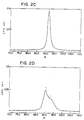
- Figures 2A, 2B, 2C and 2D are X-ray diffraction patterns of the ferroelectric liquid crystal cell of this invention.
- the axis of abscissas shows the rotation angle and the axis of ordinates, the X-ray diffraction intensity (cps).
- Figure 3 shows the relation between the apparent tilt angle ( ⁇ ) and the applied dc voltage in the ferroelectric liquid cell of this invention.
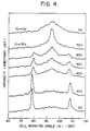
- Figure 4 shows X-ray diffraction patterns of the ferroelectric liquid crystal cell of the invention obtained at varying dc voltages applied.
- Figures 5A, 5B and 5C are sectional views of a liquid crystal cell schematically showing the layer structure of a smectic phase.
- Figure 6 is a schematic view of the molecular arrangement of the liquid crystal cell of the invention when it is viewed from above.
- Figures 7A and 7B are schematic views of the molecular arrangements of various liquid crystal phases when the liquid cell is viewed from above.
- Figures 7c shows the hysteresis of the apparent tilt angle against the pulsed voltage applied to a ferroelectric liquid crystal having no antiferroelectric phase.
- the ferroelectric liquid crystal used in this invention must have an antiferroelectric phase (S m C A *). It may be, for example, one which effects phase transition in a cooling process from an isotropic phase to a chiral nematic phase (N*), a smectic A phase (S A ), a chiral smetic C phase (S c *) and to the antiferroelectric phase (S m C A *), or one which effects phase transition from an isotropic phase, to a smectic A phase (S A ), a chiral smectric C phase (S c *) and to the antiferroelectric phase (S m C A *). But these examples are not limitative.
- the ferroelectric liquid crystal having the above phase transition is held between a pair of parallel-laid substrates having electrodes, and the liquid crystal is heated to render it in isotropic phase. Subsequent gradual cooling gives a ferroelectric liquid crystal or in the state of an antiferroelectric phase (S m C A *).
- the layer structure is of a chevron structure in the shape of " ⁇ " with respect to the substrates. By applying a voltage above a certain limit to the electrodes, the chevron structure changes to a bookshelf structure in which the liquid crystal layer is generally perpendicular to the substrates.
- the bookshelf structure changes to a chevron structure in which the title angle to the normal to the substrates is small, or a layer structure which cannot be determined to be either the chevron structure or the bookshelf structure.
- the X-ray diffraction patterns showing the above changes in layer structure are shown in Figure 4.
- the state of zig-zag defects in the layer structure was examined by observing the texture of the liquid crystal cell. Many zig-zag defects were observed before application of a voltage. But on application of a voltage, the layer structure changed to a bookshelf structure and the zig-zag defects disappeared. When the applied voltage was removed, the layer structure changed to a chevron structure in which the tilt angle to the normal to the substrates is small or a layer structure which cannot be determined readily to be a chevron or bookshelf structure. Surprisingly, no zig-zag defect was observed in this layer structure, either.
- the wave form and the frequency of the voltage to be applied there is no particular limitation in the wave form and the frequency of the voltage to be applied.
- a direct current, a rectangular wave and a triangular wave, for example, may be used as the waveform.
- the preferred frequency is 0 to 1 KHz.
- the voltage to be applied depends upon the ferroelectric liquid crystal used. But in order to change the layer structure from a chevron structure to a bookshelf structure, the voltage to be applied should be sufficiently higher than the threshold value for the director switching of liquid crystal molecules. For example, in the case of the ferroelectric liquid crystal used in Example 1 given hereinbelow, a voltage more than twice the threshold value for the director switching of the liquid crystal molecules was applied, and the layer structure completely changed to a bookshelf structure from the chevron structure.
- the bookshelf structure changes to a chevron structure having a small tilt angle to the substrates or a structure which is difficult to determine to be a chevron or bookshelf structure.
- the liquid crystal cell can actually be used in this state.
- the voltage to be applied to the electrodes of the liquid crystal cell may be slightly higher than the threshold value to the director switching of liquid crystal molecules. There is no need to make the applied voltage so high as the one applied to change the layer structure once to the bookshelf structure.
- the layer structure of the antiferroelectric phase (S m C A *) is classified to either of a chevron or bookshelf.
- the chevron structure denotes a state in which the layer of the liquid crystal is bent in the shape of " ⁇ " to the substrates.
- the bookshelf structure denotes the state in which the layer of the liquid crystal is perpencidular to the substrates as shown in Figure 5B, or the layer is tilted to the substrates as shown in Figure 5C.
- Figures 5A, 5B and 5C are sectional views of the liquid crystal cell, in which the numberal 10 represents a substrate and 12, a layer of a liquid crystal. In Figure 5A, the layer of the liquid crystal is tilted at an angle ⁇ with respect to the normal to the substrate 10.
- the X-ray diffraction pattern of the layer having a chevron structure usually has two peaks as shown in Figures 2A and 2B.
- the X-ray diffraction pattern of the layer having a bookshelf structure has a single sharp peak as shown in Figure 2C.
- the chevron structure and the bookshelf structure are defined as follows:-
- a ferroelectirc liquid crystal cell having a high contrast and a high-speed response can be obtained by applying a voltage to the electrodes and thereby changing the layer structure of the liquid crystal from a chevron structure to a bookshelf structure.
- the ferroelectric liquid crystal cell resulting from the method according to the invention shows excellent display characteristics.
- an antiferroelectric phase (S m C A *) must be present when they are subjected to phase transition from an isotropic phase in cooling process.
- the antiferroelectric phase shows the following properties.
- the extinction position of the liquid crystal cell is in a direction normal to the layer and in a direction parallel to the layer in the absence of an electric field. From this fact, it can be said that in the absence of an electric field, the long axes of the liquid crystal molecules are aligned parallel to the direction normal to the layer.
- a dc voltage above the threshold value is applied to the liquid crystal cell, the liquid crystal molecules are tilted at a certain angle from the normal to the layer, and attain a uniform state observed in an ordinary chiral smectic C phase.
- the antiferroelectric phase has the two uniform states known heretofore and one new state in which the liquid crystal molecules are apparently aligned in the direction normal to the layer.
- This new state is called a third state.
- One characteristic of the antiferroelectric phase is that it has the above three stable states (tristability). So far, much has been unknown on the detailed molecular arrangement in the antiferroelectric phase having tristability.
- a possible arrangement is shown in the model view in Figure 6 (see Japanese Journal of Applied Physics, Vol. 28, p. L 1265-1268, 1989).
- Figure 6 is taken by viewing the liquid crystal cell from above.
- the center of Figure 6 shows the third state.
- the long axes of the liquid crystal molecules are oriented in opposite directions between adjacent liquid crystal layers, and consequently, their dipole moments cancel with each other between the adjacent layers.
- the right and left end of Figure 6 show a uniform state.
- the apparent tilt angle of the liquid crystal molecules has two hysteresises with respect to a dc voltage applied, there exists a clear dc voltage threshold value, as shown in Figure 3.
- a dc electric field is applied to the electrode of the liquid crystal cell in a certain direction and the voltage is increased, the tilt angle (point A in Figure 3) which was initially 0 changes slightly until the voltage reaches near V1 (point B in Figure 3).
- the apparent tilt angle abruptly changes.
- the abrupt change of the apparent tilt angle stops point C in Figure 3
- hardly any change in tile angle occurs (point D of Figure 3).
- the tilt angle hardly changes in the initial stage.
- the appparent tilt angle begins to change (point E in Figure 3).
- the apparent tilt angle abruptly changes, and at a voltage of V4, the abrupt change of the apparent tilt angle ceases (point F in Figure 3).
- the apparent tilt angle gradually decreases, and reaches about 0 at a voltage of 0. Because of the difference between the threshold voltage V1 from the third state to the uniform state and the threshold voltage V3 from the uniform state to the third state, the apparent tilt angle shows hysteresis with respect to the dc voltage applied.
- FIGS. 7A and 7B show the relation between a liquid crystal layer 14 and liquid crystal molecules when the liquid crystal cell is viewed from above.
- the smectic A phase is a phase in which the liquid crystal molecules are aligned parallel to a direction normal to the layer.
- the extinction position in the absence of an electric field applied is in a direction normal to the layer and a direction parallel to the layer as in the case of the antiferroelectric phase (S m C A *).
- the apparent tilt angle of the liquid crystal molecules has no hysteresis with respect to the dc voltage applied, and has no threshold value relating to a dc voltage applied.
- the chiral smectic C phase is a phase in which the liquid crystal molecules are titled at an apparent tilt angle ( ⁇ ′) with respect to the normal to the layer.
- An SSFLC cell in the chiral smectic C phase has bistability, and when an electric field is applied, the liquid crystal molecules switch in a bistable state, namely between two uniform states.
- the relation between the pulsed voltage and the apparent tilt angle is such that as shown in Figure 7C, the liquid crystal molecules have a threshold voltage with respect to the pulsed voltage and a hysteresis.
- the antiferroelectric phase clearly differs from the well known smectic phases such as the smectic A phase or the chiral smectic C phase.
- Glass and plastics may be used as materials for the substrates used in this invention, and desirably transparent electrodes are disposed on the substrates.
- an organic polymeric film subjected to a rubbing treatment is formed on one or both surfaces of the substrates as an aligned film.
- the organic polymeric film are polyimide films, polyamide films and polyvinyl alcohol films.
- an inorganic film such as a film of yttrium or silicon oxide (SiO or SiO2) may be used.
- the liquid crystal may also be alingned by using the temperature gradient method in preparing a cell by holding the liquid crystal between a pair of parallel substrates, and in this case, the parallel substrates do not have to be subjected to an aligning treatment.
- the transparent electrode used in this invention is an ITO film or a NESA film.
- the distance between the parallel substrates in this invention i.e. the cell gap, varies depending upon a use to which the liquid crystal cell is put, but is preferably 0.5 to 300 micrometers. It is especially preferably 1.5 to 10 micrometers, above all 1.5 to 5 micrometers, when the cell is used as a display device.
- phase transition temperatures were 149 °C for an isotropic phase to a S m A phase, 121 °C for S m A ⁇ S m C*, 116 C* for S m C* ⁇ S m C A *, and 65 °C for S m C A * ⁇ crystal.
- a pair of ITO-coated glass substrates were coated with a polyimide, and then only one of the substrates was subjected to a rubbing treatment.
- the liquid crystal was introduced between the pair of substrates to make a liquid crysal cell.
- the cell gap was 6 micrometers.
- the liquid crystal cell was heated until the liquid crystal became an isotropic phase. Then, the liquid crystal cell was gradually cooled at a rate of 1 °C/min. to align the liquid crystal molecules parallel to the glass substrates uniformly to obtain a sample for X-ray diffractometry.
- the temperature of the liquid crystral cell was controlled by using a temperature control unit having an accuracy of ⁇ 0.1 °C.
- X-ray diffractometry was carried out by using a device Ru-200 (made by Rigaku Co., Ltd.) in accordance with the diffractometric system shown in Figure 1.
- the procedure of X-ray diffractometry was in accordance with Japanese Journal of Applied Physics, Vo. 27, PP L725, 1988 and Japanese Journal of Applied Physics, Vol. 27, PP L1993, 1988.
- the Bragg's angle of the liquid crystal was measured.
- the counter was set at the Bragg's angle.
- the cell prepared by the above procedure was rotated by an angle ⁇ , and an X-ray diffraction pattern was obtained.
- the ⁇ is an angle formed between the glass surface and an incident beam.
- the size of the X-ray beam was 1 mm2.
- X-ray diffractometry was carried out with regard to the case where the temperature of the liquid crystal cell was adjusted to 100 °C (S m C A * phase) and after aligning the liquid crystal, an electric field was never applied, to the case where an electric field was applied and the applied dc voltage was gradually increased up to 70 V, and to the case where the applied voltage was finally removed.
- the X-ray diffractometric conditions were as follows:- X-diffraction device: Ru-200, 60 kV, 200 mA Target: Cu Filter: Ni Voltage: 50 KV Current: 200 mA Scan speed: 4 deg/min. Sampling rate: 0.1 deg, continuous scan Slid: DS 0.5°, RS 0.3mm, SS 0.5° Detector: P. C.
- Figure 4 shows the X-ray diffraction patterns.
- the axis of ordinates represents the X-ray diffraction intensity and the axis of abscissas represents the rotation angle ⁇ of the liquid crystal cell.
- the threshold voltage of switching of the liquid crystal molecules was 27 V ( Figure 3, V1). From this fact, it can be seen that to convert the layer to a book-shelf structure, a voltage more than twice the threshold voltage should be applied. It is also seen that when the applied voltage is removed, the layer structure of the liquid crystal returns to the chevron structure (see the X-ray diffraction pattern of 70 ⁇ 0 V in Figure 4).
- a liquid crystal cell in which both of a pair of glass substrate were rubbed, and a liquid crystal cell in which one of a pair of glass substrates was rubbed were constructed by the same procedure as in Example 1, and by X-ray diffractometry, the layer structure of the liquid crystals were examined.
- the liquid crystal cell in which both glass substrates were rubbed was maintained at a temperature of 90 °C (S m C A * phase), and X-ray diffractometry was carried out with regard to the case where after aligning the liquid crystal, an electric field was never applied, to the case where a dc voltage of 80 V was applied, and to the case where the applied voltage was removed.
- the results are shown in Figures 2A, 2C and 2B.
- the axis of ordinates represents the X-ray diffraction intensity
- the axis of abscisssas represents the rotation angle ⁇ of the liquid crystal cell.
- the liquid crystal cell in which only one of the pair of glass substrates was rubbed was maintained at a temperature of 90 °C (S m C A * phase), and from the state where an electric field was never applied after aligning the liquid crystal, a dc voltage of 80 V was applied and then the applied voltage was removed.
- the X-ray diffraction pattern obtained at this time is shown in Figure 2D.
- Example 3 By using the liquid crystal cell obtained in Example 1 in which only one substrate was rubbed, the relation between the apparent tilt angle and the dc applied voltage was examined at 100 °C. The apparent tilt angle was taken as the angle formed between the normal to the layer and the extinction position.
- the measuring method was as follows:- A dc voltage was applied stepwise to the liquid crystal cell, and the extinction position at each voltage was observed by a polarizing microscope with a crossed polarizer, and the apparent tilt angle was determined. The results are shown in Figure 3.
- Figure 3 shows that this liquid crystal cell has a threshold value with respect to a dc voltage and memory characteristics. The threshold value with respect to the dc voltage was 27 V (V1 in Figure 3).
- Example 1 The liquid crystal cell of Example 1 in which only one substrate was rubbed was used, and the texture of the liquid crystal was observed by using a polarizing microscope with a crossed polarizer. During the microscopic observation, the liquid crystal cell was maintained at a temperature of 100 °C. Immediately after the liquid crystal molecules were aligned, many zig-zag defects were observed in the liquid crystal cell. But when a dc voltage of 70 V was applied to the cell, the zig-zag defects disappeared. When the application of the voltage was cut off, no zig-zag defects appeared again. In the cell in which zig-zag defects occurred immediately after aligning of the liquid crystal, a voltage of ⁇ 35 V having a rectangular wave form was applied, and the contrast between two unifrom states was measured.
- the contrast ratio was 35.
- a dc voltage of 70 V was applied to this cell to remove the zig-zag defects.
- a voltage of ⁇ 35 V having a rectangular wave form was again applied to it, and the contrast between the uniform states was measured.
- the contrast ratio increased to 60, showing a very high contrast.
- phase transition temperatures were 149 °C for isotropic phase ⁇ S m A phase, 121 °C for S m A ⁇ S m C*, 116 °C for S m C* ⁇ S m C A *, and 65 °C for S m C A * ⁇ crystal.
- the liquid crystal was introduced between a pair of ITO-coated glass substrates, and the liquid crystal was aligned uniformly in parallel to the substrates by the temperature gradient method.
- the cell gap was 2.5 micrometers.
- the threshold value to a dc voltage was 15 V.
- the cell was maintianed at 70 °C, and a voltage of ⁇ 17 V having a rectangular waveform and a frequency of 5Hz was applied, and the response time was measured.
- the response time was 34 microseconds.
- a dc voltage of 80 V was applied to this cell to change the layer structure to a bookshelf structure and again the above voltage was applied, the response time was 27 microseconds.
Landscapes
- Physics & Mathematics (AREA)
- Chemical & Material Sciences (AREA)
- Crystallography & Structural Chemistry (AREA)
- Nonlinear Science (AREA)
- General Physics & Mathematics (AREA)
- Optics & Photonics (AREA)
- Liquid Crystal (AREA)
Description
- This invention relates to process of eliminating zig-zag defects in a novel ferroelectric liquid crystal cell having improved display characteristics which is useful in liquid crystal display devices or liquid crystal light shutters.
- Much attention has been directed in recent years to surface stabilized ferroelectric liquid crystal (SSFLC for short) cells as electro-optical cells using ferroelectric liquid crystals. The SSFLC cells are characterized by having faster responses than conventional electro-optical cells using nematic liquid crystals and possessing bistability. This cell was developed by Clerks et al. (see US-A-4,367,924), and is said to be most likely to gain commercial acceptance. The switching theory of a director, which is an unit victor in the direction of molecular long axis, in the SSFLC cell is that when a ferroelectric liquid crystal is held in a thin cell (cell gap about 0.5 to 2 micrometers) that the helical structure of the liquid crystal disappears, a bistable state of liquid crystal molecules appears. In two stable states, the liquid crystal molecules are in two uniform states in which the directors are aligned in the different directions.
- The ferroelectric liquid crystals can lead to high-speed response characteristics and memory characteristics because they have spontaneous polarization and can have bistability. Hence, they are expected to be applicable to high-density large-screen displays and high-speed light shutters. The SSFLC cell utilizing this bistable state has recently showed a great advance with the development of liquid crystal materials. However, to utilize the SSFLC cell for dislaying on a high-density large-screen display, for example, it is necessary to improve display characteristics of the cell. For example, it should have a higher contrast, a higher-speed response, and a clearer voltage threshold value, and can achieve bistability even when the cell thickness is larger.
- Recent studies have shown that for improvements in contrast and response, the layer structure of a liquid crystal should be controlled. The layer structure of the ferroelectric liquid crystal differs depending upon the method of an aligning treatment. Generally, however, the ferroelectric liquid crystal is of a chevron structure in which the layers are bent in the shape of "<" with respect to two parallel-laid glass substrates. In many cases, by the misarrangement of the directions of the bent layers, zig-zag defects occur, and as a result of light leakage through these defects, the contrast of the cell decreases greatly. It has also been known that the response speed is higher when the layer is of the bookshelf structure than when it is of the chevron structure. Accordingly, the bookshelf structure in which the layers are generally perpendicular to the glass substrate is desired as the layer structure of a ferroelectric liquid crystal cell free from zig-zag defects.
- It is known that since generally the layer structure of conventional ferroelectric liquid crystal is not changed by an electric field, zig-zag defects do not disappear. However, there are a few examples in which zig-zag defects can be removed by an electric field, although the layer structure is not studied in detail. In these cases, it is necessary to optimize the surface treatment of substrates, cell thickness and an applied voltage in order to remove zig-zag defects.
- SiO oblique evaporation is generally known as a method of obtaining a liquid crystal cell with the liquid crystal layer having a bookshelf structure (Japanese Journal of Applied Physics, vol. 27, p. L725, 1988 and Japanese Journal of Applied Physics, vol. 27, p. L1993, 1988), but this method is difficult to practice industrially for large scale displays.
- Since the disclosure of the SSFLC cell by Clerk et al, many ferroelectric liquid crystal compounds have been synthesized. In recent years, ferroelectric liquid crystal compounds having an antiferroelectric phase (antiferroelectric liquid crystals) have attracted attention (Japanese Laid-Open Patent Publication No. 213390/1989, and Japanese Journal of Applied Physics, vol. 27,p. L729, 1988). The characteristics of antiferroelectric liquid crystals, such as their threshold voltage characteristics, the hysteresis characteristics of the apparent tilt angle (the angle formed between the normal of the liquid crystal layer and the average direction of molecular long axes) and the tristable state (two uniform states and the third state), have been known. But no information has yet been obtained on the layer structure of an antiferroelectric liquid crystal.
- The present inventors measured the relation between the tilt angle and the applied voltage in a ferroelectric liquid crystal with an antiferroelectric phase, determined the threshold dc voltage with respect to director switching in liquid crystal molecules, and analyzed the layer structure of a liquid crystal at an applied dc voltage slightly higher than the threshold voltage by using an X-ray diffraction device. They have consequently ascertained that the ferroelectric liquid crystals with an antiferroelectric phase are of the chevron structure, and by observation of their textures, many zig-zag defects are seen to exist. The ferroelectric liquid crystal cell having an antiferroelectric phase has the advantage that it has a very clear threshold value with respect to dc voltage and has memory characteristics even with a thick cell. In this regard, it may be said that the liquid crystal cell using a ferroelectrical liquid crystal having an antiferroelectric phase is much improved over liquid crystal cells using conventional ferroelectric liquid crystals. However, a layer structure of a ferroelectric liquid crystal having an antiferroelectric phase is of the chevron structure as are the conventional ferroelectric liquid crystals. To improve the contrast and response speed, it is desired to convert the layer structure of the liquid crystal to a bookshelf structure.
- It is an object of this invention therefore to provide a a method, as defined in the claim, to obtain a ferroelectirc liquid crystal cell in which the liquid crystal layer has little or no zig-zag defect.
- Still another object of this invention is to obtain a ferroelectric liquid crystal cell suitable particularly for use in a high-density large-screen display and a high-speed light shutter.
- The object of the invention is achieved by eliminating zig-zag - defects in a ferroelectric liquid crystal cell having a liquid crystal layer of a chevron structure, which comprises a ferroelectric liquid crystal having an antiferroelectric phase (SmCA*), wherein the layer structure is changed from an initial chevron structure to a bookshelf structure by application of a voltage to said layer which is about twice the switching voltage of liquid crystal molecules.
- Figure 1 is a view of an X-ray diffraction geometry used in analyzing the layer structure of a liquid in the ferroelectric liquid crystal cell of the invention. The symbols used have the following meanings.
α: the cell rotating angle
ϑ: the diffraction angle
Ki: incidnet X-rays
Ks: diffraction X rays - Figures 2A, 2B, 2C and 2D are X-ray diffraction patterns of the ferroelectric liquid crystal cell of this invention. The axis of abscissas shows the rotation angle and the axis of ordinates, the X-ray diffraction intensity (cps).
- Figure 3 shows the relation between the apparent tilt angle (⌀) and the applied dc voltage in the ferroelectric liquid cell of this invention.
- Figure 4 shows X-ray diffraction patterns of the ferroelectric liquid crystal cell of the invention obtained at varying dc voltages applied.
- Figures 5A, 5B and 5C are sectional views of a liquid crystal cell schematically showing the layer structure of a smectic phase.
- Figure 6 is a schematic view of the molecular arrangement of the liquid crystal cell of the invention when it is viewed from above.
- Figures 7A and 7B are schematic views of the molecular arrangements of various liquid crystal phases when the liquid cell is viewed from above.
- Figures 7c shows the hysteresis of the apparent tilt angle against the pulsed voltage applied to a ferroelectric liquid crystal having no antiferroelectric phase.
- The ferroelectric liquid crystal used in this invention must have an antiferroelectric phase (SmCA*). It may be, for example, one which effects phase transition in a cooling process from an isotropic phase to a chiral nematic phase (N*), a smectic A phase (SA), a chiral smetic C phase (Sc*) and to the antiferroelectric phase (SmCA*), or one which effects phase transition from an isotropic phase, to a smectic A phase (SA), a chiral smectric C phase (Sc*) and to the antiferroelectric phase (SmCA*). But these examples are not limitative.
- The ferroelectric liquid crystal having the above phase transition is held between a pair of parallel-laid substrates having electrodes, and the liquid crystal is heated to render it in isotropic phase. Subsequent gradual cooling gives a ferroelectric liquid crystal or in the state of an antiferroelectric phase (SmCA*). In this state, the layer structure is of a chevron structure in the shape of "<" with respect to the substrates. By applying a voltage above a certain limit to the electrodes, the chevron structure changes to a bookshelf structure in which the liquid crystal layer is generally perpendicular to the substrates. When the application of the voltage is stopped, the bookshelf structure changes to a chevron structure in which the title angle to the normal to the substrates is small, or a layer structure which cannot be determined to be either the chevron structure or the bookshelf structure. The X-ray diffraction patterns showing the above changes in layer structure are shown in Figure 4.
- The state of zig-zag defects in the layer structure was examined by observing the texture of the liquid crystal cell. Many zig-zag defects were observed before application of a voltage. But on application of a voltage, the layer structure changed to a bookshelf structure and the zig-zag defects disappeared. When the applied voltage was removed, the layer structure changed to a chevron structure in which the tilt angle to the normal to the substrates is small or a layer structure which cannot be determined readily to be a chevron or bookshelf structure. Surprisingly, no zig-zag defect was observed in this layer structure, either.
- In the present invention, there is no particular limitation in the wave form and the frequency of the voltage to be applied. But a direct current, a rectangular wave and a triangular wave, for example, may be used as the waveform. The preferred frequency is 0 to 1 KHz. The voltage to be applied depends upon the ferroelectric liquid crystal used. But in order to change the layer structure from a chevron structure to a bookshelf structure, the voltage to be applied should be sufficiently higher than the threshold value for the director switching of liquid crystal molecules. For example, in the case of the ferroelectric liquid crystal used in Example 1 given hereinbelow, a voltage more than twice the threshold value for the director switching of the liquid crystal molecules was applied, and the layer structure completely changed to a bookshelf structure from the chevron structure.
- In the prior art discussed above, there is no instance in which a liquid crystal cell having a book-shelf structure was obtained by the application of a voltage as in the present invention, nor an instance in which zig-zag defects are removed by changing the chevron structure to a bookshelf structure. For the first time in the art, the present invention has easily provided a liquid crystal cell with the bookshelf structure free from zig-zag defects.
- When, as described above, a voltage is applied to the liquid crystal cell to change its chevron structure to a bookshelf structure, and then the application of the voltage is stopped, the bookshelf structure changes to a chevron structure having a small tilt angle to the substrates or a structure which is difficult to determine to be a chevron or bookshelf structure. The liquid crystal cell can actually be used in this state. In actual use, the voltage to be applied to the electrodes of the liquid crystal cell may be slightly higher than the threshold value to the director switching of liquid crystal molecules. There is no need to make the applied voltage so high as the one applied to change the layer structure once to the bookshelf structure.
- Roughly, the layer structure of the antiferroelectric phase (SmCA*) is classified to either of a chevron or bookshelf. The chevron structure, as shown in Figure 5A, denotes a state in which the layer of the liquid crystal is bent in the shape of "<" to the substrates. The bookshelf structure denotes the state in which the layer of the liquid crystal is perpencidular to the substrates as shown in Figure 5B, or the layer is tilted to the substrates as shown in Figure 5C. Figures 5A, 5B and 5C are sectional views of the liquid crystal cell, in which the
numberal 10 represents a substrate and 12, a layer of a liquid crystal. In Figure 5A, the layer of the liquid crystal is tilted at an angle ψ with respect to the normal to thesubstrate 10. - It has been found that the relation between the layer structure and the X-ray diffraction pattern obtained by using the X-ray diffractometric system shown in Figure 1 is as follows. The X-ray diffraction pattern of the layer having a chevron structure usually has two peaks as shown in Figures 2A and 2B. The X-ray diffraction pattern of the layer having a bookshelf structure has a single sharp peak as shown in Figure 2C. In the present invention, the chevron structure and the bookshelf structure are defined as follows:-
- (1) When the X-ray diffraction pattern of the layer clearly has two or more peaks as shown in Figures 2A and 2B, the layer structure is a chevron structure.
- (2) When the X-ray diffraction pattern of the layer has only one sharp peak, the layer structure is a bookshelf structure.
- (3) When the X-ray diffraction pattern of the layer has two or more peaks which cannot be clearly separated, whether the layer structure is of a chevron structure or a bookshelf structure is determined by the peak width at half height of the peak of the X-ray diffraction pattern. Specifically, a sufficiently high voltage (two or more times the threshold voltage) is applied to the liquid crystal cell until an X-ray diffraction pattern is obtained which has a single sharp peak as shown in Figure 2C. In this voltage-applied state, the layer structure is a bookshelf structure. The peak width at half height (PB) of the sharp peak of the resulting X-ray diffraction pattern is measured. Next, the peak width at half height (PS) of the X-ray diffraction pattern of the layer to be determined is measured. If PS is less than two times PB, the layer structure is determined to be a bookshelf structure. If PS is two or more times PB, the layer structure is determined to be a chevron structure.
- Thus, according to the present invention described hereinabove, a ferroelectirc liquid crystal cell having a high contrast and a high-speed response can be obtained by applying a voltage to the electrodes and thereby changing the layer structure of the liquid crystal from a chevron structure to a bookshelf structure. Thus, the ferroelectric liquid crystal cell resulting from the method according to the invention shows excellent display characteristics.
- In the above-exemplified ferroelectric liquid crystal compounds or mixtures, an antiferroelectric phase (SmCA*) must be present when they are subjected to phase transition from an isotropic phase in cooling process. The antiferroelectric phase (SmCA*) shows the following properties.
- (1) The extinction position in the absence of an electric field of a liquid crystal cell aligned in parallel and having an antiferroelectric phase is in a direction normal to the layer and in a direction parallel to the layer when the liquid crystal cell is viewed from above (the direction normal to the layer and the direction parallel to the layer used in the following description denote those determined when the liquid crystal cell is viewed from above).
- (2) The apparent tilt angle (the angle formed between the direction normal to the layer and the average direction of molecular long axes) of the liquid crystal molecules in an antiferroelectric phase has hysteresis with respect to a dc voltage applied, as shown in Figure 3. Furthermore, as shown in Figure 3, this liquid crystral cell has a clear threshold value with respect to the dc voltage applied.
- (3) When a voltage above the threshold value is applied to a liquid crystal cell parallel aligned and having an antiferroelectric phase, the liquid crystal molecules attain a uniform state as is the case of the chiral smectic C phase.
- When the liquid crystal cell parallel-aligned and having an antiferroelectric phase is held between crossed polarizers and observed, the extinction position of the liquid crystal cell is in a direction normal to the layer and in a direction parallel to the layer in the absence of an electric field. From this fact, it can be said that in the absence of an electric field, the long axes of the liquid crystal molecules are aligned parallel to the direction normal to the layer. When a dc voltage above the threshold value is applied to the liquid crystal cell, the liquid crystal molecules are tilted at a certain angle from the normal to the layer, and attain a uniform state observed in an ordinary chiral smectic C phase. In other words, the antiferroelectric phase has the two uniform states known heretofore and one new state in which the liquid crystal molecules are apparently aligned in the direction normal to the layer. This new state is called a third state. One characteristic of the antiferroelectric phase is that it has the above three stable states (tristability). So far, much has been unknown on the detailed molecular arrangement in the antiferroelectric phase having tristability. A possible arrangement is shown in the model view in Figure 6 (see Japanese Journal of Applied Physics, Vol. 28, p. L 1265-1268, 1989). Figure 6 is taken by viewing the liquid crystal cell from above. The center of Figure 6 shows the third state. The long axes of the liquid crystal molecules are oriented in opposite directions between adjacent liquid crystal layers, and consequently, their dipole moments cancel with each other between the adjacent layers. The right and left end of Figure 6 show a uniform state.
- Another characteristic feature of the liquid crystal cell having an antiferroelectric phase is that the apparent tilt angle of the liquid crystal molecules has two hysteresises with respect to a dc voltage applied, there exists a clear dc voltage threshold value, as shown in Figure 3. Specifically, when a dc electric field is applied to the electrode of the liquid crystal cell in a certain direction and the voltage is increased, the tilt angle (point A in Figure 3) which was initially 0 changes slightly until the voltage reaches near V₁ (point B in Figure 3). As the voltage is further increased, the apparent tilt angle abruptly changes. When the voltage is increased to V₂, the abrupt change of the apparent tilt angle stops (point C in Figure 3), and with a further increase in voltage, hardly any change in tile angle occurs (point D of Figure 3). When the voltage begins to decrease from this state, the tilt angle hardly changes in the initial stage. When the voltage decreases to V₃, the appparent tilt angle begins to change (point E in Figure 3). When the voltage continues to be decreased, the apparent tilt angle abruptly changes, and at a voltage of V₄, the abrupt change of the apparent tilt angle ceases (point F in Figure 3). As the voltage is further decreased, the apparent tilt angle gradually decreases, and reaches about 0 at a voltage of 0. Because of the difference between the threshold voltage V₁ from the third state to the uniform state and the threshold voltage V₃ from the uniform state to the third state, the apparent tilt angle shows hysteresis with respect to the dc voltage applied. Even when the direction of the electric field applied is reversed, the same phenomenon as above occurs, although the direction of the change of the apparent tilt angle is reversed to that described above. When in Figure 3 an electric field in a reverse direction is applied and the voltage is increased and then decreased, the apparent tilt angle changes from point A → point B′→ point C′→ point D′→ point E′→ point F′→ point A. Since the apparent tilt angle abruptly changes with the change of the voltage from V₁ to V₂, a liquid crystal cell having an antiferroelectric phase (SmCA*) has a clear threshold value in dc voltage applied.
- Many smectic phases such as a smectic A phase or a chiral smectic C phase have so far been known. They differ from the antiferroelectric phase in the following respects. Figures 7A and 7B show the relation between a
liquid crystal layer 14 and liquid crystal molecules when the liquid crystal cell is viewed from above. - The smectic A phase, as shown in Figure 7A, is a phase in which the liquid crystal molecules are aligned parallel to a direction normal to the layer. In the smectic A phase, the extinction position in the absence of an electric field applied is in a direction normal to the layer and a direction parallel to the layer as in the case of the antiferroelectric phase (SmCA*). However, in the smectic A phase, the apparent tilt angle of the liquid crystal molecules has no hysteresis with respect to the dc voltage applied, and has no threshold value relating to a dc voltage applied.
- The chiral smectic C phase, as shown in Figure 7B, is a phase in which the liquid crystal molecules are titled at an apparent tilt angle (⌀′) with respect to the normal to the layer. An SSFLC cell in the chiral smectic C phase has bistability, and when an electric field is applied, the liquid crystal molecules switch in a bistable state, namely between two uniform states. The relation between the pulsed voltage and the apparent tilt angle is such that as shown in Figure 7C, the liquid crystal molecules have a threshold voltage with respect to the pulsed voltage and a hysteresis. The antiferroelectric phase clearly differs from the well known smectic phases such as the smectic A phase or the chiral smectic C phase.
- Glass and plastics, for example, may be used as materials for the substrates used in this invention, and desirably transparent electrodes are disposed on the substrates. Desirably, an organic polymeric film subjected to a rubbing treatment is formed on one or both surfaces of the substrates as an aligned film. Examples of the organic polymeric film are polyimide films, polyamide films and polyvinyl alcohol films. Instead of the organic polymeric film, an inorganic film such as a film of yttrium or silicon oxide (SiO or SiO₂) may be used. The liquid crystal may also be alingned by using the temperature gradient method in preparing a cell by holding the liquid crystal between a pair of parallel substrates, and in this case, the parallel substrates do not have to be subjected to an aligning treatment.
- Preferably, the transparent electrode used in this invention is an ITO film or a NESA film.
- The distance between the parallel substrates in this invention, i.e. the cell gap, varies depending upon a use to which the liquid crystal cell is put, but is preferably 0.5 to 300 micrometers. It is especially preferably 1.5 to 10 micrometers, above all 1.5 to 5 micrometers, when the cell is used as a display device.
- The following Examples illustrate the present invention more specifically.
- 4-(1-Methylheptyloxycarbonyl)phenyl 4′-octyloxybiphenyl-4-carboxylate was used as a liquid crystal. The phase transition temperatures were 149 °C for an isotropic phase to a SmA phase, 121 °C for SmA → Sm C*, 116 C* for SmC* → SmCA*, and 65 °C for SmCA* → crystal.
- A pair of ITO-coated glass substrates were coated with a polyimide, and then only one of the substrates was subjected to a rubbing treatment. The liquid crystal was introduced between the pair of substrates to make a liquid crysal cell. The cell gap was 6 micrometers. The liquid crystal cell was heated until the liquid crystal became an isotropic phase. Then, the liquid crystal cell was gradually cooled at a rate of 1 °C/min. to align the liquid crystal molecules parallel to the glass substrates uniformly to obtain a sample for X-ray diffractometry. The temperature of the liquid crystral cell was controlled by using a temperature control unit having an accuracy of ±0.1 °C.
- X-ray diffractometry was carried out by using a device Ru-200 (made by Rigaku Co., Ltd.) in accordance with the diffractometric system shown in Figure 1. The procedure of X-ray diffractometry was in accordance with Japanese Journal of Applied Physics, Vo. 27, PP L725, 1988 and Japanese Journal of Applied Physics, Vol. 27, PP L1993, 1988. Specifically, by using a capillary cell filled with the liquid crystal, the Bragg's angle of the liquid crystal was measured. Then, the counter was set at the Bragg's angle. The cell prepared by the above procedure was rotated by an angle α, and an X-ray diffraction pattern was obtained. The α is an angle formed between the glass surface and an incident beam. The size of the X-ray beam was 1 mm². X-ray diffractometry was carried out with regard to the case where the temperature of the liquid crystal cell was adjusted to 100 °C (SmCA* phase) and after aligning the liquid crystal, an electric field was never applied, to the case where an electric field was applied and the applied dc voltage was gradually increased up to 70 V, and to the case where the applied voltage was finally removed.
- The X-ray diffractometric conditions were as follows:-
X-diffraction device: Ru-200, 60 kV, 200 mA
Target: Cu
Filter: Ni
Voltage: 50 KV
Current: 200 mA
Scan speed: 4 deg/min.
Sampling rate: 0.1 deg, continuous scan
Slid: DS 0.5°, RS 0.3mm, SS 0.5°
Detector: P. C. - Figure 4 shows the X-ray diffraction patterns. In Figure 4, the axis of ordinates represents the X-ray diffraction intensity and the axis of abscissas represents the rotation angle α of the liquid crystal cell. It is seen from Figure 4 that as the applied voltage is increased, the layer structure of the liquid crystal changed from the chevron structure to a bookshelf structure. The threshold voltage of switching of the liquid crystal molecules was 27 V (Figure 3, V₁). From this fact, it can be seen that to convert the layer to a book-shelf structure, a voltage more than twice the threshold voltage should be applied. It is also seen that when the applied voltage is removed, the layer structure of the liquid crystal returns to the chevron structure (see the X-ray diffraction pattern of 70 → 0 V in Figure 4).
- A liquid crystal cell in which both of a pair of glass substrate were rubbed, and a liquid crystal cell in which one of a pair of glass substrates was rubbed were constructed by the same procedure as in Example 1, and by X-ray diffractometry, the layer structure of the liquid crystals were examined. The liquid crystal cell in which both glass substrates were rubbed was maintained at a temperature of 90 °C (SmCA* phase), and X-ray diffractometry was carried out with regard to the case where after aligning the liquid crystal, an electric field was never applied, to the case where a dc voltage of 80 V was applied,
and to the case where the applied voltage was removed. The results are shown in Figures 2A, 2C and 2B. In these figures, the axis of ordinates represents the X-ray diffraction intensity, and the axis of abscisssas represents the rotation angle α of the liquid crystal cell.
The liquid crystal cell in which only one of the pair of glass substrates was rubbed was maintained at a temperature of 90 °C (SmCA* phase), and from the state where an electric field was never applied after aligning the liquid crystal, a dc voltage of 80 V was applied and then the applied voltage was removed. The X-ray diffraction pattern obtained at this time is shown in Figure 2D. It is seen from Figure 2D and the X-ray difraction pattern of 70 → 0 V of Figure 4 that the X-ray diffraction pattern of the liquid crystal cell having a cheveron structure (only one substrate was rubbed), which was measured after removing the applied voltage, varied to some extent depending upon the cells. Figures 2B and 2D show that the X-ray diffraction pattern of the liquid crystal cell having a chevron structure after removing of the applied electric field greatly differs depending upon the substrate rubbing conditions. - By using the liquid crystal cell obtained in Example 1 in which only one substrate was rubbed, the relation between the apparent tilt angle and the dc applied voltage was examined at 100 °C. The apparent tilt angle was taken as the angle formed between the normal to the layer and the extinction position. The measuring method was as follows:- A dc voltage was applied stepwise to the liquid crystal cell, and the extinction position at each voltage was observed by a polarizing microscope with a crossed polarizer, and the apparent tilt angle was determined. The results are shown in Figure 3. Figure 3 shows that this liquid crystal cell has a threshold value with respect to a dc voltage and memory characteristics. The threshold value with respect to the dc voltage was 27 V (V₁ in Figure 3).
- The liquid crystal cell of Example 1 in which only one substrate was rubbed was used, and the texture of the liquid crystal was observed by using a polarizing microscope with a crossed polarizer. During the microscopic observation, the liquid crystal cell was maintained at a temperature of 100 °C. Immediately after the liquid crystal molecules were aligned, many zig-zag defects were observed in the liquid crystal cell. But when a dc voltage of 70 V was applied to the cell, the zig-zag defects disappeared. When the application of the voltage was cut off, no zig-zag defects appeared again. In the cell in which zig-zag defects occurred immediately after aligning of the liquid crystal, a voltage of ±35 V having a rectangular wave form was applied, and the contrast between two unifrom states was measured. The contrast ratio was 35. A dc voltage of 70 V was applied to this cell to remove the zig-zag defects. Then, a voltage of ±35 V having a rectangular wave form was again applied to it, and the contrast between the uniform states was measured. The contrast ratio increased to 60, showing a very high contrast.
- 4-(1-mehylheptyloxycarbonyl)phenyl 4′-octyloxybiphenyl-4-carboxylate was used as a liquid crystal. The phase transition temperatures were 149 °C for isotropic phase → SmA phase, 121 °C for SmA → SmC*, 116 °C for SmC* → SmCA*, and 65 °C for SmCA* → crystal. The liquid crystal was introduced between a pair of ITO-coated glass substrates, and the liquid crystal was aligned uniformly in parallel to the substrates by the temperature gradient method. The cell gap was 2.5 micrometers. In this liquid crystal cell, the threshold value to a dc voltage was 15 V. The cell was maintianed at 70 °C, and a voltage of ±17 V having a rectangular waveform and a frequency of 5Hz was applied, and the response time was measured. When the above voltage was applied to the cell to which an electric field was never applied after aligning the liquid crystal, the response time was 34 microseconds. On the other hand, when a dc voltage of 80 V was applied to this cell to change the layer structure to a bookshelf structure and again the above voltage was applied, the response time was 27 microseconds. By changing the chevron structure to the bookshelf structure by application of an electric field, the response speed was increased.
In the ferroelectric liquid crystal cell obtained from the invention, switching between two uniform states can be performed at a high speed while retaining a bookshelf structure. It is assumed that the director switching between two uniform states in the ferroelectric liquid crystal cell obtained from this invention proceeds by the same mechanism as in the case of switching between two uniform states in a chiral smectic C phase. The layer structure in the conventional chiral smectic C phase has a chevron structure and the mechanism of its director switching is known in detail. Japanese Journal of Applied Physics, Vol. 26, pp. L21-24, 1987 states that director switching betweeen two uniform states proceeds at a higher speed when the layer structure is of a bookshelf structure than when it is of a chevron structure. However, there has been no practical method of easily making a liquid crystal cell in which the layer structure in the conventional chiral smectic C phase attains a bookshelf structure. In contrast, according to this invention, the layer structure of a liquid crystal can be easily changed from a chevron sructure to a bookshelf structure by application of a voltage. Accordingly, a liquid crystal cell in which director switching between two uniform states can be performed at a high speed can be made easily.
Claims (1)
- A process of eliminating zig-zag-defects which are caused by the misarrangement of the directions of the bent layers in a ferroelectric liquid crystal cell having a liquid crystal layer of a chevron structure, which comprises a ferroelectric liquid crystal having an antiferroelectric phase (SmCA*), wherein the layer structure is changed from an initial chevron structure to a bookshelf structure by application of a voltage to said layer which is about twice the threshold switching voltage of said liquid crystal layer.
Applications Claiming Priority (2)
| Application Number | Priority Date | Filing Date | Title |
|---|---|---|---|
| JP28117588 | 1988-11-09 | ||
| JP281175/88 | 1988-11-09 |
Publications (3)
| Publication Number | Publication Date |
|---|---|
| EP0368305A2 EP0368305A2 (en) | 1990-05-16 |
| EP0368305A3 EP0368305A3 (en) | 1990-10-31 |
| EP0368305B1 true EP0368305B1 (en) | 1994-10-26 |
Family
ID=17635395
Family Applications (1)
| Application Number | Title | Priority Date | Filing Date |
|---|---|---|---|
| EP89120773A Expired - Lifetime EP0368305B1 (en) | 1988-11-09 | 1989-11-09 | Ferroelectric liquid crystal cell |
Country Status (3)
| Country | Link |
|---|---|
| US (1) | US5078477A (en) |
| EP (1) | EP0368305B1 (en) |
| DE (1) | DE68919044T2 (en) |
Families Citing this family (25)
| Publication number | Priority date | Publication date | Assignee | Title |
|---|---|---|---|---|
| US5293544A (en) * | 1989-03-07 | 1994-03-08 | Canon Kabushiki Kaisha | Liquid crystal apparatus including panel having plural bent layers of liquid crystal molecules |
| DE69107646T2 (en) * | 1990-04-04 | 1995-08-24 | Mitsubishi Gas Chemical Co | Liquid crystalline compound and liquid crystal display device. |
| JP2982330B2 (en) * | 1990-04-28 | 1999-11-22 | ソニー株式会社 | Liquid crystal display device |
| EP0484849B1 (en) * | 1990-11-05 | 1994-08-31 | Mitsubishi Gas Chemical Company, Inc. | Optically active alcohol, process for producing same and liquid crystal compound using same |
| JP3039571B2 (en) * | 1991-06-04 | 2000-05-08 | 三菱瓦斯化学株式会社 | Liquid crystal composition |
| JPH04359990A (en) * | 1991-06-06 | 1992-12-14 | Mitsui Petrochem Ind Ltd | Liquid crystal composition, its use, and its manufacture |
| JPH05249435A (en) * | 1992-03-03 | 1993-09-28 | Mitsubishi Gas Chem Co Inc | Antiferroelectric liquid crystal element |
| JP2651972B2 (en) * | 1992-03-04 | 1997-09-10 | 株式会社半導体エネルギー研究所 | Liquid crystal electro-optical device |
| JPH05271658A (en) * | 1992-03-27 | 1993-10-19 | Chisso Corp | Antiferroelectric liquid crystal composition |
| JP3456493B2 (en) * | 1992-10-24 | 2003-10-14 | ソニー株式会社 | Liquid crystal element |
| JP3471851B2 (en) | 1993-05-06 | 2003-12-02 | 株式会社半導体エネルギー研究所 | Liquid crystal display |
| US5589966A (en) * | 1993-05-11 | 1996-12-31 | Mitsui Petrochemical Industries, Ltd. | Antiferroelectric liquid crystal light modulation device |
| JPH06347796A (en) * | 1993-06-02 | 1994-12-22 | Canon Inc | Liquid crystal device |
| US5510914A (en) * | 1993-11-15 | 1996-04-23 | The Regents Of The University Of Colorado | Smectic liquid crystal analog phase modulator |
| US6008787A (en) * | 1995-04-07 | 1999-12-28 | Citizen Watch Co., Ltd. | Antiferrolectric liquid crystal panel and method for driving same |
| JPH08286190A (en) * | 1995-04-10 | 1996-11-01 | Hoechst Ind Kk | Production of ferroelectric liquid crystal element |
| JPH09146126A (en) * | 1995-11-22 | 1997-06-06 | Canon Inc | Liquid crystal device and information transmission device |
| KR0177975B1 (en) * | 1995-12-26 | 1999-05-01 | 윤종용 | Twisted Structure Antiferroelectric Liquid Crystal Display |
| JP3106166B2 (en) * | 1996-01-25 | 2000-11-06 | 株式会社デンソー | Liquid crystal cell |
| JPH10307285A (en) * | 1997-05-08 | 1998-11-17 | Casio Comput Co Ltd | Liquid crystal display device and driving method thereof |
| CN1180289C (en) * | 1998-03-10 | 2004-12-15 | 西铁城时计株式会社 | Antiferroelectric liquid crystal display and its driving method |
| SE517919C2 (en) * | 1998-07-08 | 2002-08-06 | Ecsibeo Ab | Liquid crystal device and method for its preparation and use |
| US6084649A (en) * | 1998-08-10 | 2000-07-04 | 3M Innovative Properties Company | Tristable liquid crystal display device |
| JP4880838B2 (en) * | 2001-09-05 | 2012-02-22 | 株式会社東芝 | Method and apparatus for assembling liquid crystal display device |
| SE0200910D0 (en) * | 2002-03-22 | 2002-03-22 | Ecsibeo Ab | A liquid crystal device, a method for producing a liquid crystal device and a method for controlling liquid crystal device |
Family Cites Families (1)
| Publication number | Priority date | Publication date | Assignee | Title |
|---|---|---|---|---|
| CA1258512A (en) * | 1985-10-28 | 1989-08-15 | John W. Goodby | Ferroelectric liquid crystal optical devices |
-
1989
- 1989-11-08 US US07/433,261 patent/US5078477A/en not_active Expired - Fee Related
- 1989-11-09 EP EP89120773A patent/EP0368305B1/en not_active Expired - Lifetime
- 1989-11-09 DE DE68919044T patent/DE68919044T2/en not_active Expired - Fee Related
Also Published As
| Publication number | Publication date |
|---|---|
| EP0368305A3 (en) | 1990-10-31 |
| DE68919044D1 (en) | 1994-12-01 |
| US5078477A (en) | 1992-01-07 |
| DE68919044T2 (en) | 1995-05-18 |
| EP0368305A2 (en) | 1990-05-16 |
Similar Documents
| Publication | Publication Date | Title |
|---|---|---|
| US5078477A (en) | Ferroelectric liquid crystal cell | |
| JP2558405B2 (en) | Gray scale display | |
| US5790223A (en) | Ferroelectric liquid crystal device and treatment method therefor | |
| EP0032362A1 (en) | Chiral smectic liquid crystal electro-optical device and process of making the same | |
| JPH04258924A (en) | Chiral smectic liquid crystal device and its manufacturing method | |
| US5200848A (en) | Ferroelectric smectic liquid crystal device | |
| Rudquist et al. | Tilt plane orientation in antiferroelectric liquid crystal cells and the origin of the pretransitional effect | |
| US5825447A (en) | Liquid crystal device with a bistable chiral smectic liquid crystal having a phase transition series lacking a cholesteric phase #16 | |
| JPH09146126A (en) | Liquid crystal device and information transmission device | |
| Oh-e et al. | X-ray studies on layer structure and bistability in ferroelectric liquid crystals | |
| Jagemalm et al. | Temperature induced anchoring transition in nematic liquid crystals with two-fold degenerate alignment | |
| JP2932531B2 (en) | Liquid crystal device using antiferroelectric phase | |
| Goodby et al. | Ferroelectric switching in the tilted smectic phases OF R-(-)-4-n-Hexyloxybenzylidene 4'-AMINO-(2-Chloropropyl) cinnamate (HOBACPC) | |
| JPH0448368B2 (en) | ||
| CA2077132C (en) | Liquid crystal display | |
| Yadav et al. | Smectic layer reorientation by surface mode in surface stabilized ferroelectric liquid crystal | |
| Demikhov | Surface and bulk periodical structures in smectic-C films with one free boundary | |
| JP3076085B2 (en) | Liquid crystal electro-optical device | |
| JP3083016B2 (en) | Liquid crystal alignment treatment method and liquid crystal element manufacturing method | |
| Kuwahara et al. | A method for molecular alignment of ferroelectric smectic liquid crystal: combination of metal oxide thin film and electric field | |
| JP3254204B2 (en) | Cell with smectic liquid crystal | |
| JP2547974B2 (en) | Smectic liquid crystal device and manufacturing method thereof | |
| Raja et al. | Temperature effect on the rubbing-induced optical phase retardation of a side group liquid crystalline polymer film | |
| Findon et al. | An unusual chevron structure in an achiral smectic C liquid crystal device | |
| JPH0451022A (en) | Liquid crystal alignment method |
Legal Events
| Date | Code | Title | Description |
|---|---|---|---|
| PUAI | Public reference made under article 153(3) epc to a published international application that has entered the european phase |
Free format text: ORIGINAL CODE: 0009012 |
|
| AK | Designated contracting states |
Kind code of ref document: A2 Designated state(s): DE FR GB |
|
| PUAL | Search report despatched |
Free format text: ORIGINAL CODE: 0009013 |
|
| AK | Designated contracting states |
Kind code of ref document: A3 Designated state(s): DE FR GB |
|
| 17P | Request for examination filed |
Effective date: 19901212 |
|
| 17Q | First examination report despatched |
Effective date: 19921001 |
|
| GRAA | (expected) grant |
Free format text: ORIGINAL CODE: 0009210 |
|
| AK | Designated contracting states |
Kind code of ref document: B1 Designated state(s): DE FR GB |
|
| REF | Corresponds to: |
Ref document number: 68919044 Country of ref document: DE Date of ref document: 19941201 |
|
| ET | Fr: translation filed | ||
| PLBE | No opposition filed within time limit |
Free format text: ORIGINAL CODE: 0009261 |
|
| STAA | Information on the status of an ep patent application or granted ep patent |
Free format text: STATUS: NO OPPOSITION FILED WITHIN TIME LIMIT |
|
| 26N | No opposition filed | ||
| PGFP | Annual fee paid to national office [announced via postgrant information from national office to epo] |
Ref country code: FR Payment date: 19981110 Year of fee payment: 10 |
|
| PGFP | Annual fee paid to national office [announced via postgrant information from national office to epo] |
Ref country code: DE Payment date: 19981116 Year of fee payment: 10 |
|
| PGFP | Annual fee paid to national office [announced via postgrant information from national office to epo] |
Ref country code: GB Payment date: 19991103 Year of fee payment: 11 |
|
| PG25 | Lapsed in a contracting state [announced via postgrant information from national office to epo] |
Ref country code: FR Free format text: LAPSE BECAUSE OF NON-PAYMENT OF DUE FEES Effective date: 20000731 |
|
| PG25 | Lapsed in a contracting state [announced via postgrant information from national office to epo] |
Ref country code: DE Free format text: LAPSE BECAUSE OF NON-PAYMENT OF DUE FEES Effective date: 20000901 |
|
| REG | Reference to a national code |
Ref country code: FR Ref legal event code: ST |
|
| PG25 | Lapsed in a contracting state [announced via postgrant information from national office to epo] |
Ref country code: GB Free format text: LAPSE BECAUSE OF NON-PAYMENT OF DUE FEES Effective date: 20001109 |
|
| GBPC | Gb: european patent ceased through non-payment of renewal fee |
Effective date: 20001109 |