EP0366141A1 - Integrated circuit for vehicle - Google Patents
Integrated circuit for vehicle Download PDFInfo
- Publication number
- EP0366141A1 EP0366141A1 EP89119996A EP89119996A EP0366141A1 EP 0366141 A1 EP0366141 A1 EP 0366141A1 EP 89119996 A EP89119996 A EP 89119996A EP 89119996 A EP89119996 A EP 89119996A EP 0366141 A1 EP0366141 A1 EP 0366141A1
- Authority
- EP
- European Patent Office
- Prior art keywords
- connector
- connector housing
- integrated circuit
- circuit board
- holes
- Prior art date
- Legal status (The legal status is an assumption and is not a legal conclusion. Google has not performed a legal analysis and makes no representation as to the accuracy of the status listed.)
- Granted
Links
Images


Classifications
-
- H—ELECTRICITY
- H05—ELECTRIC TECHNIQUES NOT OTHERWISE PROVIDED FOR
- H05K—PRINTED CIRCUITS; CASINGS OR CONSTRUCTIONAL DETAILS OF ELECTRIC APPARATUS; MANUFACTURE OF ASSEMBLAGES OF ELECTRICAL COMPONENTS
- H05K5/00—Casings, cabinets or drawers for electric apparatus
- H05K5/0026—Casings, cabinets or drawers for electric apparatus provided with connectors and printed circuit boards [PCB], e.g. automotive electronic control units
- H05K5/0043—Casings, cabinets or drawers for electric apparatus provided with connectors and printed circuit boards [PCB], e.g. automotive electronic control units comprising a frame housing mating with two lids wherein the PCB is flat mounted on the frame housing
-
- H—ELECTRICITY
- H05—ELECTRIC TECHNIQUES NOT OTHERWISE PROVIDED FOR
- H05K—PRINTED CIRCUITS; CASINGS OR CONSTRUCTIONAL DETAILS OF ELECTRIC APPARATUS; MANUFACTURE OF ASSEMBLAGES OF ELECTRICAL COMPONENTS
- H05K5/00—Casings, cabinets or drawers for electric apparatus
- H05K5/0026—Casings, cabinets or drawers for electric apparatus provided with connectors and printed circuit boards [PCB], e.g. automotive electronic control units
- H05K5/0069—Casings, cabinets or drawers for electric apparatus provided with connectors and printed circuit boards [PCB], e.g. automotive electronic control units having connector relating features for connecting the connector pins with the PCB or for mounting the connector body with the housing
Definitions
- the present invention relates to an integrated circuit for a vehicle, in which a conductive layer is formed on a conductive substrate through an insulating layer so as to fix circuit elements.
- a method of manufacturing an IC disclosed in this prior art comprises the steps of: anodic-oxidizing at least one major surface of an aluminum substrate to form an aluminum oxide thin layer on the surface of the substrate; selectively depositing a resistive material layer and a conductive material layer on the aluminum oxide thin layer to form a plurality of circuit elements; fixing a transistor pellet onto a lead portion formed by selectively depositing the conductive material layer; and sealing at least all the circuit elements with an insulating resin.
- the IC formed in this manner may be adopted for use in a vehicle in view of a compact structure and low cost.
- it when such an IC is actually used in a vehicle, it must be reliably connected to other control portions of a vehicle while effectively utilizing its compact and low-cost advantages. If an existing connecting device is used, it is relatively large and is expensive. Thus, even if the IC itself is made compact and reduced in cost, its merit cannot be satisfactorily utilized.
- the present invention has been made in consideration of the above situation, and has as its principal object to provide an integrated circuit for a vehicle, in which a conductive foil is adhered on a conductive substrate through an insulating layer to fix circuit elements, and which can be rendered compact and can reduce cost when it is used in a vehicle.
- an integrated circuit for a vehicle comprises: a pair of circuit boards, each circuit board including: a metal circuit board main body; an insulating layer formed on an entire surface of the circuit board main body; a conductive layer formed on the insulating layer in a predetermined circuit pattern; and a plurality of circuit elements electrically connected to a predetermined portion of the conductive layer; and externally connecting connector means electrically connected to another connector, the externally connecting connector means comprising: a connector housing fixed to the circuit boards and having a recess for receiving the another connector, a plurality of through holes being formed in the connector housing; and a plurality of connector pins, one-end portions of which are connected to connecting terminals formed at an edge portion of the conductive layer, middle portions of which extend through the through holes formed in the connector housing, and the other-end portions of which project into the recess.
- an integrated circuit for a vehicle comprises: a pair of circuit boards, each circuit board including: a metal circuit board main body; an insulating layer formed on an entire surface of the circuit board main body; a conductive layer formed on the insulating layer in a predetermined circuit pattern; and a plurality of circuit elements electrically connected to a predetermined portion of the conductive layer; and externally connecting connector means electrically connected to another connector, wherein one functional component for a vehicle is constituted by an independent integrated circuit, and the circuit board main body of the circuit board is defined as a functional component case.
- a connector housing of an integrated circuit includes: a pair of connector housing halves respectively fixed to the circuit boards before the circuit boards are assembled to oppose each other, and having a plurality of connector pins connected to the corresponding conductive layers; and superposition means which are respectively formed on the connector housing halves and are superposed on each other so as to constitute one connector housing when the circuit boards are assembled to oppose each other.
- the connector housing of the integrated circuit is fixed in advance on one circuit board before the circuit boards are assembled to oppose each other
- the connector pins include first connector pins mounted in advance in the connector housing to be inserted thereto before the assembly, and second connector pins electrically and mechanically connected to connecting terminals formed at an edge portion of the conductive layer of the other circuit board
- the externally connecting connector means further includes a mounting portion which is formed on the connector housing and to which the second connector pins are mounted when the circuit boards are assembled to oppose each other.
- an integrated circuit for a vehicle comprises: a pair of circuit boards, each circuit board including: a metal circuit board main body; an insulating layer formed on an entire surface of the circuit board main body; a conductive layer formed on the insulating layer in a predetermined circuit pattern; and a plurality of circuit elements electrically connected to a predetermined portion of the conductive layer; and externally connecting connector means electrically connected to another connector, wherein a plurality of the integrated circuits are formed to have independent control functions, and further comprising: a connecting box to which the plurality of integrated circuits are simultaneously mounted through the corresponding externally connecting connector means to be electrically connected thereto; and multiplex transmission means, arranged in the connecting box, for connecting the plurality of integrated circuits and portions to be controlled through multiplex transmission.
- Fig. 1 shows an IC 10 for a vehicle according to the present invention.
- the IC 10 is arranged as an independent functional component for a vehicle. More specifically, the IC 10 is arranged as an IC independently having a function as an engine control unit.
- the IC 10 is formed as a closed box-like case.
- a male connector 12 as a connecting device is integrally attached to one end portion of the IC 10.
- the male connector 12 is connected to a conventional female connector 14 as will be described in detail later.
- the IC 10 comprises a pair of lower and upper circuit boards 16a and 16b which are separated from each other, a side plate 18 for vertically separating the circuit boards 16a and 16b by a predetermined interval and closing side surfaces, and a frame 20 for integrally fixing the circuit boards 16a and 16b and the side plate 18.
- circuit elements such as an IC chip necessary for providing a function as an engine control unit arranged as an independent functional component for a vehicle, resistors, capacitors, and the like are mounted on the circuit boards 16a and 16b.
- the circuit boards 16a and 16b are formed by splitting one common circuit board 22 into two boards. More specifically, as shown in Fig.
- the common circuit board 22 is formed by a circuit board body 22a formed of a conductive material, e.g., aluminum, an insulating layer 22b adhered over the entire upper surface of the circuit board body 22a, a conductive foil 22c formed on the insulating layer 22b to have a predetermined circuit pattern and to define a circuit network, and a large number of circuit elements 22d electrically connected to predetermined portions of the conductive foil 22c.
- a circuit board body 22a formed of a conductive material, e.g., aluminum
- an insulating layer 22b adhered over the entire upper surface of the circuit board body 22a
- a conductive foil 22c formed on the insulating layer 22b to have a predetermined circuit pattern and to define a circuit network
- a large number of circuit elements 22d electrically connected to predetermined portions of the conductive foil 22c.
- a vertical opening 22e is preformed in the central portion of the common circuit board 22.
- Right and left circuit network portions to have the opening 22e as a boundary are connected to each other through a flexible circuit board 22f extending over the opening 22e.
- Upper and lower edges (regions indicated by reference symbols X and Y) including upper and lower ends of the opening 22e are cut off, so that the pair of circuit boards 16a and 16b are formed while being connected through the flexible circuit board 22f.
- a plurality of connecting terminals 22g and 22h (which are arranged so that their polarities are inverted for every other terminals) are linearly formed along an edge portion on the upper surface of the outer edge portion of the circuit board 16a to be located at a lower position (the left circuit board in Fig. 4A), i.e., on an inner surface of an edge portion defining one end of the case in a state wherein the circuit boards are vertically separated from each other.
- Connecting pins 24a and 24b of the male connector 12 (to be described later) are fixed to and electrically connected to these connecting terminals 22g and 22h to extend outwardly.
- the side plate 18 is formed to have a U-shape with one open side when viewed from the above, and is set so that the open side portion serves as one end of the case. Stepped portions 18a and 18b for receiving three edge portions of the corresponding circuit boards 16a and 16b are formed on the inner side edges of the lower and upper end faces of the side plate 18.
- the circuit boards 16a and 16b are fitted in the corresponding stepped portions 18a and 18b through seal rubbers 26. Upon insertion of the seal rubbers 26, entrance of dust into the case from gaps between these components can be prevented.
- the frame is formed to vertically clamp and surround the side surfaces closed by the side plate 18.
- the frame 20 is formed integrally with a main body 20a facing the side plate 18, and flange portions 20b and 20C extending inwardly by a predetermined distance (that is, a distance long enough to clamp three closed side edges of the lower and upper circuit boards 16a and 16b).
- the frame 20 is formed to vertically clamp the lower and upper circuit boards 16a and 16b fitted in the lower and upper stepped portions of the side plate 18, thus integrally constituting the case.
- the flexible circuit board 22f for connecting the circuit elements 22d of the lower and upper circuit boards 16a and 16b is set to be located inside from the other end portion of the side plate 18.
- the circuit boards 16a and 16b can be kept assembled to be vertically separated by the predetermined distance in a state wherein the side plate 18 is interposed therebetween.
- the IC 10 is formed into a case shape, and the lower and upper surfaces of the case are directly defined by the circuit boards 16a and 16b.
- the IC 10 can be rendered compact and lightweight as compared to a case wherein the circuit boards 16a and 16b are housed in separate cases.
- the connecting device comprises the male connector 12 attached to a one-end opening portion of the case-like IC 10 in a so-called internal mounting state, and the female connector 14 detachably connected to the male connector 12.
- the male connector 12 comprises a connector main body 28 formed into a box-like housing with one open side surface.
- the connector main body 28 is designed to be just fitted in the one-end opening portion of the case-like IC 10. In the fitting state, the connector main body 28 is fixed to the IC 10 by screws or the like.
- the connector main body 28 has a recess 30 for receiving the female connector 14 in its side surface at one end side.
- the connector main body 28 has an upright segment 28a for just closing the one-end opening portion of the case-like IC 10 on its side surface at the other end side.
- a plurality of pairs of through holes 28b and 28c which are vertically separated from each other are formed in the upright segment 28a to be aligned along a lateral direction. For this reason, the connecting pins 24a connected to every other connecting terminals 22g of the connecting terminals 22g and 22h extend through the upper through holes 28b, and the connecting pins 24b connected to the remaining connecting terminals 22h extend through the lower through holes 28c while being deviated sideways.
- each connecting pin 24b extending through the lower through hole 28c becomes smaller than that of the connecting pin 24a extending through the upper through hole 28b.
- a so-called arch portion 32 having a round middle portion is formed. With the arch portion 32, the length of each connecting pins 24b extending through the lower through hole 28c is set to be substantially the same as that of the connecting pin 24a extending through the upper through hole 28b, and these pins exhibit the same heat dissipation effect.
- a vertical distance l between these connecting pins 24a and 24b and a pitch p of horizontally adjacent pins are determined based on conventional pin arrangement specifications.
- a pair of female connectors 14 connected to the male connector 12 can be of a conventional type, thus providing an economical advantage.
- a conventional male connector is heavy in weight and large in size, it is not employed, and an exclusive male connector 12 is formed in correspondence with the compact and lightweight case-like IC 10. Therefore, according to the first embodiment, the compact and lightweight structure of the IC 10 can be prevented from being impaired.
- the IC 10 of the first embodiment is arranged to define lower and upper surfaces by the pair of circuit boards 16a and 16b. As a result, according to the first embodiment, the number of parts of the IC 10 can be reduced, thus achieving a compact and low-cost IC.
- each of the circuit boards 16a and 16b is formed to have the aluminum conductive circuit board body 22a, the insulating layer 22b adhered on the circuit board body 22a, and the conductive foil 22c adhered on the insulating layer 22b to have a predetermined pattern.
- the IC 10 serves as the engine control unit.
- the present invention is not limited to this.
- the IC 10 may be arranged to be operated as independent functional components for a vehicle, such as an automatic-speed controller, a four-wheel steering controller, an automatic transmission controller, and the like.
- the flexible circuit board 22f is located in a space surrounded by the side plate 18.
- the present invention is not limited to this.
- a segment 18c of the side plate 18 just facing an opening surface is displaced forward (toward the opening) by a predetermined distance from the rear ends of the circuit boards 16a and 16b, so that the flexible circuit board 22f may extend between the segment 18c and the frame 20.
- the lower and upper circuit boards 16a and 16b are fitted in the lower and upper stepped portions 18a and 18b of the side plate 18, and this assembly is surrounded by the frame 20 from the outer side to integrally form the case-like IC 10.
- the present invention is not limited to this.
- the lower and upper circuit boards 16a and 16b are fitted in the lower and upper stepped portions 18a and 18b of the side plate 18, and their contact surfaces are adhered to each other by an adhesive Z, thus integrally constituting the case-like IC 10 without using the frame 20.
- the connecting terminals 22g and 22h are alternately and laterally aligned at the opening edge of the lower circuit board 16a in the first embodiment described above.
- the connecting terminals may be arranged as shown in Fig. 8 showing the second embodiment.
- connecting terminals 22g and 22h are aligned in two, i.e., rear and front arrays at the opening edge of a lower circuit board 16a.
- the rear connecting terminals 22g (farther side from the male connector 12) are aligned to define an array different from that defined by the front connecting terminals 22h (nearer side to the male connector 12).
- Connecting pins 24a connected to the rear connecting terminals 22g extend through upper through holes 28b, and connecting pins 24b connected to the front connecting terminals 22h extend through lower through holes 28c.
- each connecting pin 24a connected to the front connecting terminal 22h becomes smaller than that of the connecting pin 24b connected to the rear connecting terminal 22g, an arch portion 32 is formed in a middle portion of the shorter connecting terminal 24b like in the first embodiment.
- the second embodiment is arranged as described above, the same effect as in the first embodiment can be provided, and the number of connecting pins 24a and 24b can be increased.
- connecting terminals 22g and 22h are juxtaposed on the lower circuit board 16a.
- the present invention is not limited to this.
- the connecting terminals may be arranged as shown in Fig. 9 showing one modification of the second embodiment.
- one set of the connecting terminals 22g are aligned on the upper circuit board 16b, and the other set of the connecting terminals 22h are aligned on the lower circuit board 16a.
- a connecting operation of the connecting pins 24a and 24b and the corresponding connecting terminals 22g and 22h i.e., a soldering operation can be facilitated.
- the upper through holes 28b are formed in substantially the central portion of the upright segment 28a, and the lower through holes 28c are formed in the lower portion of the upright segment 28a.
- the length of each connecting pin 24b connected to the other connecting terminal 22h becomes shorter than that of the connecting pin 24a connected to one connecting terminal 22g.
- an arch portion 32 is formed in a middle portion of the connecting pin 24b connected to the other connecting terminal 22h.
- the connecting pins 24a and 24b are connected and fixed to the corresponding connecting terminals 22g and 22h by directly soldering them.
- the present invention is not limited to this.
- these pins and terminals may be connected as shown in Fig. 10 showing another modification of the second embodiment.
- the connecting pins 24a and 24b are linearly formed, and extend through and are fixed to the through holes 28a and 28b while being vertically stacked and aligned in two arrays in the lateral direction.
- the connecting pins 24a and 24b and the corresponding connecting terminals 22g and 22h are connected to each other through bonding wires 34. Note that the connecting terminals 22g and 22h are aligned in two, i.e., front and rear arrays on the lower circuit board 16a as in the second embodiment described above.
- the male connector 12 is arranged as a so-called internal mounting type with respect to the case-like IC 10.
- the present invention is not limited to this arrangement, and the male connector 12 may be arranged as shown in Fig. 11 showing the third embodiment.
- a male connector 12 is arranged as a so-called external mounting type. More specifically, the male connector 12 is constituted by a connector main body 28′ which is formed to have a substantially U-shaped section, and to extend along one edge of an IC 10 to close the one-end opening, and a plurality of pairs of connecting pins 24a and 24b which are aligned in the lateral direction to be vertically separated from each other.
- the connector main body 28′ is formed of an insulating material, e.g., plastic to integrally have an upright segment 28a′ which is located to close the one-end opening of the case-like IC 10 and through which the connecting pins 24a and 24b extend, a pair of upper and lower connecting segments 28b′ and 28c′, extending from the upper and lower edges of the upright segment 28a in a direction opposite to the IC 10, for protecting the connecting pins 24a and 24b extending through the upright segment 28a′ and for defining a recess 30 for receiving the above-mentioned female connector 14, and a pair of upper and lower mounting segments 28d′ and 28e′, extending from the upper and lower edges of the upright segment 28a′ toward the IC 10 and fixed to the upper and lower side surfaces of one-end portions of a pair of upper and lower circuit boards 16b and 16a of the IC 10 while being in sliding contact therewith.
- an insulating material e.g., plastic
- connecting terminals comprise one set of connecting terminals 22g aligned on the upper circuit board 16b and the other set of connecting terminals 22h aligned on the lower circuit board 16b as has been described in one modification of the second embodiment shown in Fig. 9.
- a plurality of through holes 28f′ and 28g′ for receiving a plurality of linear connecting pins 24a and 24b are preformed in the upright segment 28a′.
- the lower and upper ends of a common circuit board 22 are cut off while these connecting pins 24a and 24b are soldered to the connecting terminals 22g and 22h of the common circuit board 22, thus providing the pair of circuit boards 16a and 16b.
- these connecting pins 24a and 24b are inserted through the through holes 28f′ and 28g′. In this manner, the connector main body 28′ is mounted on the case-like IC 10 in an external mounting state.
- the compact and low-cost case-like IC 10 can be realized as in the first and second embodiments.
- the lower and upper circuit boards 16a and 16b are mounted on the lower and upper surfaces of the external mounting type male connector 12.
- the male connector may be arranged as shown in Fig. 12 showing one modification of the third embodiment.
- the one-end portions of the lower and upper circuit boards 16a and 16b are bent downward and upward, respectively, to integrally have outer flange portions 22i and 22j.
- the pair of mounting segments 28d′ and 28e′ of the male connector 12 are fixed to surfaces of the outer flange portions 22i and 22j opposite thereto, so that the male connector 12 is integrally mounted on the case-like IC 10.
- the connecting pins 24a and 24b used for the male connectors 12 are linearly formed like in the third embodiment.
- the present invention is not limited to this.
- the connecting pins may be formed as shown in Fig. 13 showing another modification of the third embodiment.
- each of the connecting pins 24a and 24b has a stepped portion at its middle portion, and an end portion connected to a corresponding connecting terminal 22g or 22h is folded back at 180°.
- connection with the female connector 14 may often be unsuccessful, and then the connecting pins 24a and 24b abut against the end face of the female connector 14 and are pushed inwardly.
- the connecting pins 24a and 24b are pushed inwardly, the connecting pins 24a and 24b are disengaged from the corresponding connecting terminals 22g and 22h since they have the linear shape as described above.
- the connecting pins 24a and 24b are satisfactorily deformed on the basis of the shape of the connecting pins 24a and 24b, and can be prevented from being disengaged from the connecting pins 22g and 22h.
- an IC used for a vehicle according to the present invention in which a conductive foil is adhered on a conductive circuit board through an insulating layer to fix circuit elements, can also be considered as an invention characterized in that one functional component for a vehicle is constituted by independent ICs and the conductive circuit board is formed as a functional component case.
- the present invention since one functional component for a vehicle is constituted by independent ICs and the conductive circuit board is formed as the functional component case, the entire structure can be rendered light in weight, and an expensive conventional connecting device need not be used, thus reducing cost.
- the fourth embodiment will be described below with reference to Figs. 14 and 15.
- the above-mentioned IC is applied to a system (called a total wiring system; to be abbreviated as a TWS hereinafter) which totally connects signal systems used for an antitheft system, a lamp flashing system, an operating system of wipers, and the like in a joint box (connecting box), and connects a control system to the joint box to control the above systems.
- a total wiring system to be abbreviated as a TWS hereinafter
- Fig. 14 shows a joint box 40 used in the fourth embodiment.
- the joint box 40 is detachably connected to a plurality of logic modules, i.e., first and second ICs 44 and 46 in the fourth embodiment through first and second connector mechanisms 48 and 50 while a conventional TWS control unit is divided in units of modules.
- each of the ICs 44 and 46 is basically the same as that of the IC 10 described in the first embodiment, and a description thereof will be omitted.
- the ICs 44 and 46 have different control contents in independent functional components for a vehicle.
- the first control circuit (IC) 44 comprises a control circuit 44a for executing a function of an antitheft system constituted as one independent functional component for a vehicle, and a first multiplex communication interface circuit 44b for connecting the control circuit 44a, and an external portion to be controlled and an external detection portion through multiplex transmission.
- the second control circuit (IC) 46 comprises a control circuit 46a for executing a function of a lamp flashing system as another independent functional component for a vehicle, and a second multiplex communication interface circuit 46b for connecting the control circuit 46a, and an external portion to be controlled and an external detection portion through multiplex transmission.
- the first connector mechanism 48 comprises a first male connector 48a integrally formed on the first IC 44, and a first female connector 48b integrally mounted on the joint box 40 to be detachable with the first male connector 48a.
- the second connector mechanism 50 comprises a second male connector 50a integrally formed on the second IC 46, and a second female connector 50b integrally mounted on the joint box 40 to be detachable with the second male connector 50a.
- the first and second connectors 48a and 50a have the same shape as that of the male connector 12 in the first embodiment.
- the first and second female connectors 48b and 50b have the same shapes as in the first embodiment.
- the first male connector 48a integrally mounted on the first IC 44 can be connected to the second female connector 50b, while the second male connector 50a integrally mounted on the second IC 46 can be connected to the first female connector 48b.
- a multiplex unit 56 is connected to the joint box 40 by a multiplex harness 54 through a third connector mechanism 52.
- the third connector mechanism 52 comprises a third male connector 52a to which a one-end portion of the multiplex harness 54 is connected, and a third female connector 52b integrally mounted on the joint box 40 to be detachable with the male connector 52a.
- the first to third connector mechanisms 48, 50, and 52 are connected to transmit multiplexed signals, as will be described later.
- Connecting terminals of each connector mechanism are formed to include four poles, i.e., terminals for a power supply, one bus line, the other bus line, and ground.
- the joint box 40 is also connected to lamps and a horn as portions to be controlled by the first and second ICs 44 and 46, various sensors as detection portions, a battery as a power source, and the like through fourth to sixth connector mechanisms 58, 60, and 62.
- the fourth to sixth connector mechanisms 58, 60, and 62 respectively comprise male connectors 58a, 60a, and 62a to which one-end portions of harnesses 64, 66, and 68 connected to corresponding portions are connected, and female connectors 58b, 60b, and 62b integrally formed on the joint box 40 to be detachable with these male connectors 58a, 60a, and 62a.
- the fourth to sixth connector mechanisms 58, 60, and 62 are arranged to connect non-multiplexed signals, and the number of connecting terminals of these mechanisms is independently determined in accordance with the number of devices to be connected and the like.
- a multiplex interface circuit 70 for converting multiplexed data into non-multiplexed data and vice versa is arranged in the joint box 40 to which the various connector mechanisms are connected.
- the multiplex interface circuit 70 comprises a multiplex terminal group for inputting/outputting multiplexed data, and a non-multiplex terminal group for inputting/outputting non-multiplexed data.
- the multiplex terminal group includes four poles, i.e., terminals for a power supply, one bus line, the other bus line, and ground, as described above, and is independently connected to corresponding terminals of the first to third female connectors 48b, 50b, and 52b. That is, the multiplex interface circuit 70 and each of the first to third female connectors 48b, 50b, and 52b are connected through four connecting lines.
- the non-multiplex terminal group is connected to corresponding terminals of the fourth to sixth female connectors 58b, 60b, and 62b through a plurality of connecting lines.
- the first and second ICs 44 and 46 are connected to the joint box 40 of the fourth embodiment with the above arrangement, as shown in Fig. 15.
- the fourth embodiment since a conventional male connector is heavy in weight and large in size, it is not employed, and the exclusive male connectors 48a and 50a are formed in correspondence with the compact and lightweight case-like IC 44. Therefore, the fourth embodiment can contribute to a compact structure of the joint box 40 based on the compact and lightweight ICs 44 and 46.
- each of the ICs 44 and 46 constituting the logic modules is arranged to have the metal circuit board body 22a.
- the compact and lightweight ICs 44 and 46 can realize the compact joint box 40 connected thereto.
- the connector housing (main body) 28 is formed of an integral member.
- the present invention is not limited to this arrangement but may be arranged, as shown in Figs. 16 to 19 showing the fifth embodiment.
- a male connector 12 of the fifth embodiment comprises a connector housing 28 formed into a box-like housing with one open side surface, as shown in Fig. 16.
- the connector housing 28 is just fitted in the one-end opening portion of a case-like IC 10 as in the above embodiments.
- the connector housing 28 is constituted by vertically coupling two split, i.e., upper and lower connector housing halves 28a and 28b. More specifically, the upper connector housing half 28a is fixed to the lower surface of a one-end portion of an upper circuit board 16b by screws (not shown), and the lower connector housing half 28b is fixed to the upper surface of a one-end portion of a lower circuit board 16a by screws (not shown).
- the upper connector housing half 28a is formed to have a size larger than the lower connector housing half 28b.
- a recess 80 for receiving the lower connector housing half 28b from below is formed in the lower surface of the upper connector housing half 28a.
- a plurality of downwardly projecting bosses 82 are formed on a surface for defining the upper bottom surface of the recess 80.
- a plurality of recesses 84 for complementarily receiving these bosses 82 are formed in the upper surface of the lower connector housing half 28b.
- Vertical guide grooves 86 are formed in the two side surfaces of the recess 80. Ridges 88 which are complementarily fitted in the guide grooves 86 are formed on two side surfaces of the lower connector housing half 28b. Upon engagement of these guide grooves 86 and the ridges 88, a relative position between the connector housing halves 28a and 28b when they are assembled to each other can be defined. These halves can be precisely guided to an engagement position defined by the bosses 82 and the recesses 84. After assembly, parallelness between the two circuit boards 16a and 16b can be accurately defined.
- Mounting holes 90a and 90b for receiving connecting pins 24a and 24b to extend therethrough are formed in the upper and lower connector housing halves 28a and 28b, respectively.
- the connecting pins 24a and 24b prior to assembly of the connector housing halves 28a and 28b, are mounted in and fixed to the corresponding mounting holes 90a and 90b of the upper and lower connector housing halves 28a and 28b to extend therethrough.
- the corresponding connecting pins 24a and 24b have already been mounted on these connector housing halves 28a and 28b.
- the connecting pins 24a and 24b are soldered to corresponding connecting terminals 22g and 22h in an open state of the circuit boards 16a and 16b.
- the soldering operation requires a fine operation since there are a large number of connecting terminals 22g and 22h.
- the soldering operation can be reliably executed, thus improving workability, and maintaining a good assembly property.
- the circuit board 16a which is to be located at a lower position is held in position, and the circuit board 16b to be located at an upper position is lifted up and moved to be parallel to the lower circuit board 16a thereabove.
- the ridges 88 are fitted in the guide grooves 86 to be guided along them, and the upper circuit board 16b is then pushed down.
- the lower connector housing half 28b is fitted in the recess 80 of the upper connector housing half 28a.
- the upper and lower housing halves are integrated upon fitting of the bosses 82 and the recesses 84.
- the circuit boards 16a and 16b are set to be parallel to each other.
- a side plate 18 is attached, and a frame 20 is fitted, thus forming the IC 10 integrally with the male connector 12, as shown in Fig. 1.
- the connector housing 28 of the male connector 12 is formed by the two split connector housing halves 28a and 28b.
- the connector housing halves 28a and 28b are fixed to the corresponding circuit boards 16a and 16b, respectively, and the connecting pins 24a and 24b are connected to the corresponding connecting terminals 22g and 22h. In this manner, a new effect of maintaining the good assembly property of the IC 10 can be provided.
- the connector housing 28 is split into halves to maintain the good assembly property.
- the present invention is not limited to this arrangement.
- a male connector 12 may be split into one set of connecting pins 24a and a connector housing 28 to which the other set of connecting pins 24b are mounted in advance, as shown in Fig. 20 showing the sixth embodiment.
- the male connector 12 comprises an integrally formed connector housing 28 unlike in the fifth embodiment wherein the connector 12 comprises the two split connector housing halves 28a and 28b.
- the connector housing 28 has the same shape as an integrated shape of the connector housing halves 28a and 28b in the fifth embodiment.
- Upper and lower mounting holes 90a and 90b for receiving the connecting pins 24a and 24b are formed in the housing 28 to be aligned in two arrays.
- the connecting pins 24b are mounted in advance in the lower connecting holes 90b of the connector housing 28.
- the male connector 12 is split into two sections, i.e., one set of connecting pins 24a and the connector housing 28 to which the other set of the connecting pins 24b are mounted in advance.
- two circuit boards 16a and 16b are formed in an open state on a plane like in the fifth embodiment.
- One set of connecting pins 24a are connected to connecting terminals 22h of the circuit board 16b to be located at an upper position.
- the connector housing 28 to which the other set of connecting pins 24b are mounted in advance is fixed to the circuit board 16a to be located at a lower position, and the other set of connecting pins 24b are connected to connecting terminals 22g of the circuit board 16a.
- one circuit board 16a is held in position, and the other circuit board 16b is lifted up and moved to be parallel to the lower circuit board 16a thereabove.
- One set of connecting pins 24a connected to the other circuit board 16b are inserted in and fixed to the mounting holes 90a formed in the connector housing 28 fixed to one circuit board 16a.
- the connector housing 28 of the male connector 12 is formed with the other set of connecting pins 24b mounted in advance, and one set of connecting pins 24a are mounted to be connected to the connecting terminals 22h of the other circuit board 16b.
- the other circuit board 16b is fixed to the connector housing.
- a good assembly property of the IC 10 can be maintained.
Abstract
Description
- The present invention relates to an integrated circuit for a vehicle, in which a conductive layer is formed on a conductive substrate through an insulating layer so as to fix circuit elements.
- As a conventional integrated circuit (IC) in which a conductive foil is adhered to a conductive substrate through an insulating layer to fix circuit elements, a technique disclosed in Japanese Patent Publication No. 46-13234 is known. A method of manufacturing an IC disclosed in this prior art comprises the steps of: anodic-oxidizing at least one major surface of an aluminum substrate to form an aluminum oxide thin layer on the surface of the substrate; selectively depositing a resistive material layer and a conductive material layer on the aluminum oxide thin layer to form a plurality of circuit elements; fixing a transistor pellet onto a lead portion formed by selectively depositing the conductive material layer; and sealing at least all the circuit elements with an insulating resin.
- In an IC formed in this manner, heat generated by a resistor, a transistor, or the like can be quickly and effectively dissipated, so that an output circuit, or the like can be formed as an IC.
- The IC formed in this manner may be adopted for use in a vehicle in view of a compact structure and low cost. However, when such an IC is actually used in a vehicle, it must be reliably connected to other control portions of a vehicle while effectively utilizing its compact and low-cost advantages. If an existing connecting device is used, it is relatively large and is expensive. Thus, even if the IC itself is made compact and reduced in cost, its merit cannot be satisfactorily utilized.
- Even if a connecting device is rendered compact, if it has a poor assembly property, it is often impossible to assemble the connecting device in practice. Therefore, the assembly property must be sufficiently taken into consideration.
- The present invention has been made in consideration of the above situation, and has as its principal object to provide an integrated circuit for a vehicle, in which a conductive foil is adhered on a conductive substrate through an insulating layer to fix circuit elements, and which can be rendered compact and can reduce cost when it is used in a vehicle.
- It is another object of the present invention to provide an integrated circuit for a vehicle which can be rendered compact, can reduce cost, and can provide a good assembly property.
- It is still another object of the present invention to provide an integrated circuit for a vehicle, which can make compact an arrangement of a connecting box connected to the integrated circuit.
- In order to achieve the principal object of the present invention, according to a first aspect of the present invention, an integrated circuit for a vehicle, comprises:
a pair of circuit boards, each circuit board including:
a metal circuit board main body; an insulating layer formed on an entire surface of the circuit board main body; a conductive layer formed on the insulating layer in a predetermined circuit pattern; and a plurality of circuit elements electrically connected to a predetermined portion of the conductive layer; and
externally connecting connector means electrically connected to another connector,
the externally connecting connector means comprising:
a connector housing fixed to the circuit boards and having a recess for receiving the another connector, a plurality of through holes being formed in the connector housing; and
a plurality of connector pins, one-end portions of which are connected to connecting terminals formed at an edge portion of the conductive layer, middle portions of which extend through the through holes formed in the connector housing, and the other-end portions of which project into the recess. - In order to achieve the principal object of the present invention, according to a second aspect of the present invention, an integrated circuit for a vehicle, comprises:
a pair of circuit boards, each circuit board including:
a metal circuit board main body; an insulating layer formed on an entire surface of the circuit board main body; a conductive layer formed on the insulating layer in a predetermined circuit pattern; and a plurality of circuit elements electrically connected to a predetermined portion of the conductive layer; and
externally connecting connector means electrically connected to another connector,
wherein one functional component for a vehicle is constituted by an independent integrated circuit, and
the circuit board main body of the circuit board is defined as a functional component case. - In order to achieve the above-mentioned other object of the present invention, according to a third aspect of the present invention, a connector housing of an integrated circuit includes:
a pair of connector housing halves respectively fixed to the circuit boards before the circuit boards are assembled to oppose each other, and having a plurality of connector pins connected to the corresponding conductive layers; and
superposition means which are respectively formed on the connector housing halves and are superposed on each other so as to constitute one connector housing when the circuit boards are assembled to oppose each other. - In order to achieve the above-mentioned other object of the present invention, according to a fourth aspect of the present invention,
the connector housing of the integrated circuit is fixed in advance on one circuit board before the circuit boards are assembled to oppose each other,
the connector pins include first connector pins mounted in advance in the connector housing to be inserted thereto before the assembly, and second connector pins electrically and mechanically connected to connecting terminals formed at an edge portion of the conductive layer of the other circuit board, and
the externally connecting connector means further includes a mounting portion which is formed on the connector housing and to which the second connector pins are mounted when the circuit boards are assembled to oppose each other. - In order to achieve the above-mentioned still other object of the present invention, according to a fifth aspect of the present invention, an integrated circuit for a vehicle comprises:
a pair of circuit boards, each circuit board including:
a metal circuit board main body; an insulating layer formed on an entire surface of the circuit board main body; a conductive layer formed on the insulating layer in a predetermined circuit pattern; and a plurality of circuit elements electrically connected to a predetermined portion of the conductive layer; and
externally connecting connector means electrically connected to another connector,
wherein a plurality of the integrated circuits are formed to have independent control functions, and
further comprising:
a connecting box to which the plurality of integrated circuits are simultaneously mounted through the corresponding externally connecting connector means to be electrically connected thereto; and
multiplex transmission means, arranged in the connecting box, for connecting the plurality of integrated circuits and portions to be controlled through multiplex transmission. - Other features and advantages of the present invention will be apparent from the following description taken in conjunction with the accompanying drawings, in which like reference characters designate the same or similar parts throughout the figures thereof.
-
- Fig. 1 is a perspective view showing an arrangement of the first embodiment of an integrated circuit for a vehicle according to the present invention;
- Fig. 2 is an exploded perspective view showing an arrangement of the integrated circuit shown in Fig. 1;
- Fig. 3A is a sectional view taken along a line A - A in Fig. 1;
- Fig. 3B is a sectional view taken along a line B - B in Fig. 1;
- Fig. 4A is a plan view showing an arrangement of a common circuit board;
- Fig. 4B is a sectional view showing an arrangement of the common circuit board;
- Fig. 5 is a sectional view showing an arrangement of a male connector attached to the integrated circuit;
- Fig. 6 is a sectional view showing an arrangement of a modification of the integrated circuit of the first embodiment;
- Fig. 7 is a sectional view showing an arrangement of another modification of the integrated circuit of the first embodiment;
- Fig. 8 is a sectional view showing an arrangement of the second embodiment of an integrated circuit according to the present invention;
- Fig. 9 is a sectional view showing an arrangement of a modification of the integrated circuit of the second embodiment;
- Fig. 10 is a sectional view showing an arrangement of another modification of the integrated circuit of the second embodiment;
- Fig. 11 is a sectional view showing an arrangement of the third embodiment of an integrated circuit according to the present invention;
- Fig. 12 is a sectional view showing an arrangement of a modification of the integrated circuit of the third embodiment;
- Fig. 13 is a sectional view showing an arrangement of another modification of the integrated circuit of the third embodiment;
- Fig. 14 is a block diagram showing an arrangement of the fourth embodiment in which an integrated circuit according to the present invention is applied to a TWS;
- Fig. 15 is a perspective view showing in detail a state wherein two types of integrated circuits in the TWS shown in Fig. 14 are connected to a joint box;
- Fig. 16 is a sectional view showing an arrangement of a male connector adopted in an arrangement of the fifth embodiment of an integrated circuit according to the present invention;
- Fig. 17 is a front view showing a state immediately before upper and lower connector housing halves constituting a connector housing shown in Fig. 16 are engaged with each other;
- Fig. 18 is a top view showing a state wherein the connector housing halves shown in Fig. 17 are fixed to open circuit boards;
- Fig. 19 is a side view showing a state wherein the circuit boards to which the connector housing halves shown in Fig. 17 are fixed are being assembled to each other; and
- Fig. 20 is a side view showing an arrangement of the sixth embodiment of an integrated circuit according to the present invention.
- An arrangement of the first embodiment of an integrated circuit (IC) for a vehicle according to the present invention will be described in detail below with reference to the accompanying drawings.
- Fig. 1 shows an
IC 10 for a vehicle according to the present invention. TheIC 10 is arranged as an independent functional component for a vehicle. More specifically, theIC 10 is arranged as an IC independently having a function as an engine control unit. - As shown in Fig. 1, the
IC 10 is formed as a closed box-like case. Amale connector 12 as a connecting device is integrally attached to one end portion of theIC 10. Themale connector 12 is connected to a conventionalfemale connector 14 as will be described in detail later. - As shown in Figs. 2 to 3B, the
IC 10 comprises a pair of lower andupper circuit boards side plate 18 for vertically separating thecircuit boards frame 20 for integrally fixing thecircuit boards side plate 18. - More specifically, circuit elements such as an IC chip necessary for providing a function as an engine control unit arranged as an independent functional component for a vehicle, resistors, capacitors, and the like are mounted on the
circuit boards circuit boards common circuit board 22 into two boards. More specifically, as shown in Fig. 4B, thecommon circuit board 22 is formed by acircuit board body 22a formed of a conductive material, e.g., aluminum, an insulatinglayer 22b adhered over the entire upper surface of thecircuit board body 22a, aconductive foil 22c formed on the insulatinglayer 22b to have a predetermined circuit pattern and to define a circuit network, and a large number ofcircuit elements 22d electrically connected to predetermined portions of theconductive foil 22c. - As shown in Fig. 4A, a
vertical opening 22e is preformed in the central portion of thecommon circuit board 22. Right and left circuit network portions to have theopening 22e as a boundary are connected to each other through aflexible circuit board 22f extending over theopening 22e. Upper and lower edges (regions indicated by reference symbols X and Y) including upper and lower ends of theopening 22e are cut off, so that the pair ofcircuit boards flexible circuit board 22f. - A plurality of connecting
terminals circuit board 16a to be located at a lower position (the left circuit board in Fig. 4A), i.e., on an inner surface of an edge portion defining one end of the case in a state wherein the circuit boards are vertically separated from each other. Connectingpins terminals - The
side plate 18 is formed to have a U-shape with one open side when viewed from the above, and is set so that the open side portion serves as one end of the case. Steppedportions corresponding circuit boards side plate 18. - As shown in Fig. 3A, the
circuit boards portions seal rubbers 26. Upon insertion of the seal rubbers 26, entrance of dust into the case from gaps between these components can be prevented. - As shown in Fig. 2, the frame is formed to vertically clamp and surround the side surfaces closed by the
side plate 18. Theframe 20 is formed integrally with amain body 20a facing theside plate 18, andflange portions 20b and 20C extending inwardly by a predetermined distance (that is, a distance long enough to clamp three closed side edges of the lower andupper circuit boards - As shown in Fig. 3B, the
frame 20 is formed to vertically clamp the lower andupper circuit boards side plate 18, thus integrally constituting the case. As shown in Fig. 3B, theflexible circuit board 22f for connecting thecircuit elements 22d of the lower andupper circuit boards side plate 18. - Since the
frame 20 is formed in this manner, thecircuit boards side plate 18 is interposed therebetween. - More specifically, in the first embodiment, the
IC 10 is formed into a case shape, and the lower and upper surfaces of the case are directly defined by thecircuit boards IC 10 can be rendered compact and lightweight as compared to a case wherein thecircuit boards - The structure of a connecting device for connecting the case-
like IC 10 with the above arrangement to a portion to be connected of a vehicle will be described below with reference to Fig. 5. - The connecting device comprises the
male connector 12 attached to a one-end opening portion of the case-like IC 10 in a so-called internal mounting state, and thefemale connector 14 detachably connected to themale connector 12. Themale connector 12 comprises a connectormain body 28 formed into a box-like housing with one open side surface. The connectormain body 28 is designed to be just fitted in the one-end opening portion of the case-like IC 10. In the fitting state, the connectormain body 28 is fixed to theIC 10 by screws or the like. - The connector
main body 28 has arecess 30 for receiving thefemale connector 14 in its side surface at one end side. The connectormain body 28 has anupright segment 28a for just closing the one-end opening portion of the case-like IC 10 on its side surface at the other end side. A plurality of pairs of throughholes upright segment 28a to be aligned along a lateral direction. For this reason, the connectingpins 24a connected to every other connectingterminals 22g of the connectingterminals holes 28b, and the connectingpins 24b connected to the remaining connectingterminals 22h extend through the lower throughholes 28c while being deviated sideways. - Note that the length of each connecting
pin 24b extending through the lower throughhole 28c becomes smaller than that of the connectingpin 24a extending through the upper throughhole 28b. In order to provide a length large enough to dissipate heat upon soldering of the connectingpins 24b to the connectingterminals 22h, a so-calledarch portion 32 having a round middle portion is formed. With thearch portion 32, the length of each connecting pins 24b extending through the lower throughhole 28c is set to be substantially the same as that of the connectingpin 24a extending through the upper throughhole 28b, and these pins exhibit the same heat dissipation effect. - When the
arch portion 32 is formed in the connectingpin 24b extending through the lower throughhole 28c, since it serves as a shock absorber, a shock upon connection of the connectors can be sufficiently absorbed as well as the above-mentioned heat dissipation effect, and the connectingpins 24b can be prevented from being disengaged from the corresponding connectingterminals 22g. - In the first embodiment, a vertical distance ℓ between these connecting
pins female connectors 14 connected to themale connector 12 can be of a conventional type, thus providing an economical advantage. - Since a conventional male connector is heavy in weight and large in size, it is not employed, and an exclusive
male connector 12 is formed in correspondence with the compact and lightweight case-like IC 10. Therefore, according to the first embodiment, the compact and lightweight structure of theIC 10 can be prevented from being impaired. - As described above, the
IC 10 of the first embodiment is arranged to define lower and upper surfaces by the pair ofcircuit boards IC 10 can be reduced, thus achieving a compact and low-cost IC. - In the first embodiment, each of the
circuit boards circuit board body 22a, the insulatinglayer 22b adhered on thecircuit board body 22a, and theconductive foil 22c adhered on the insulatinglayer 22b to have a predetermined pattern. As a result, since heat generated by thevarious circuit elements 22d can be dissipated by utilizing the aluminumcircuit board body 22a as a heat dissipation plate, a separate heat dissipation member need not be arranged, thus greatly making the structure compact. - In the first embodiment, as described above, since the lower and upper surfaces of the case are respectively defined by the pair of
circuit boards circuit board body 22a, thesecircuit boards like IC 10 can be substantially electromagnetically shielded, and thecircuit elements 22d are not easily influenced by an electromagnetic wave. - The present invention is not limited to the arrangement of the first embodiment, and various changes and modifications may be made within the spirit and scope of the invention.
- Various embodiments and modifications of the present invention will be described below. In the modifications and other embodiments, the same reference numerals denote the same parts as in the arrangement of the first embodiment, and a detailed description thereof will be omitted.
- For example, in the description of the first embodiment, the
IC 10 serves as the engine control unit. However, the present invention is not limited to this. For example, theIC 10 may be arranged to be operated as independent functional components for a vehicle, such as an automatic-speed controller, a four-wheel steering controller, an automatic transmission controller, and the like. - In the first embodiment, as shown in Fig. 3B, the
flexible circuit board 22f is located in a space surrounded by theside plate 18. However, the present invention is not limited to this. As shown in Fig. 6 showing one modification of the first embodiment, asegment 18c of theside plate 18 just facing an opening surface is displaced forward (toward the opening) by a predetermined distance from the rear ends of thecircuit boards flexible circuit board 22f may extend between thesegment 18c and theframe 20. - In the first embodiment, the lower and
upper circuit boards portions side plate 18, and this assembly is surrounded by theframe 20 from the outer side to integrally form the case-like IC 10. However, the present invention is not limited to this. For example, as shown in Fig. 7 showing another modification of the first embodiment, the lower andupper circuit boards portions side plate 18, and their contact surfaces are adhered to each other by an adhesive Z, thus integrally constituting the case-like IC 10 without using theframe 20. - The connecting
terminals lower circuit board 16a in the first embodiment described above. However, the present invention is not limited to this. The connecting terminals may be arranged as shown in Fig. 8 showing the second embodiment. - In the second embodiment shown in Fig. 8, connecting
terminals lower circuit board 16a. The rear connectingterminals 22g (farther side from the male connector 12) are aligned to define an array different from that defined by the front connectingterminals 22h (nearer side to the male connector 12). Connectingpins 24a connected to the rear connectingterminals 22g extend through upper throughholes 28b, and connectingpins 24b connected to the front connectingterminals 22h extend through lower throughholes 28c. - Since the length of each connecting
pin 24a connected to the front connecting terminal 22h becomes smaller than that of the connectingpin 24b connected to therear connecting terminal 22g, anarch portion 32 is formed in a middle portion of the shorter connecting terminal 24b like in the first embodiment. - Since the second embodiment is arranged as described above, the same effect as in the first embodiment can be provided, and the number of connecting
pins - In the second embodiment, two arrays of connecting
terminals lower circuit board 16a. However, the present invention is not limited to this. For example, the connecting terminals may be arranged as shown in Fig. 9 showing one modification of the second embodiment. - As shown in Fig. 9, in the modification of the second embodiment, one set of the connecting
terminals 22g are aligned on theupper circuit board 16b, and the other set of the connectingterminals 22h are aligned on thelower circuit board 16a. With this arrangement, in this modification, a connecting operation of the connectingpins terminals - In this modification, the upper through
holes 28b are formed in substantially the central portion of theupright segment 28a, and the lower throughholes 28c are formed in the lower portion of theupright segment 28a. As a result, the length of each connectingpin 24b connected to the other connecting terminal 22h becomes shorter than that of the connectingpin 24a connected to one connectingterminal 22g. As a result, for the same reason as in the modification described above, anarch portion 32 is formed in a middle portion of the connectingpin 24b connected to the other connecting terminal 22h. - In the second embodiment and its modification, the connecting
pins terminals - As shown in Fig. 10, in another modification of the second embodiment, the connecting
pins holes terminals bonding wires 34. Note that the connectingterminals lower circuit board 16a as in the second embodiment described above. - In the first and second embodiments, the
male connector 12 is arranged as a so-called internal mounting type with respect to the case-like IC 10. However, the present invention is not limited to this arrangement, and themale connector 12 may be arranged as shown in Fig. 11 showing the third embodiment. - As shown in Fig. 11, a
male connector 12 according to the third embodiment of the present invention is arranged as a so-called external mounting type. More specifically, themale connector 12 is constituted by a connectormain body 28′ which is formed to have a substantially U-shaped section, and to extend along one edge of anIC 10 to close the one-end opening, and a plurality of pairs of connectingpins - More specifically, the connector
main body 28′ is formed of an insulating material, e.g., plastic to integrally have anupright segment 28a′ which is located to close the one-end opening of the case-like IC 10 and through which the connectingpins segments 28b′ and 28c′, extending from the upper and lower edges of theupright segment 28a in a direction opposite to theIC 10, for protecting the connectingpins upright segment 28a′ and for defining arecess 30 for receiving the above-mentionedfemale connector 14, and a pair of upper andlower mounting segments 28d′ and 28e′, extending from the upper and lower edges of theupright segment 28a′ toward theIC 10 and fixed to the upper and lower side surfaces of one-end portions of a pair of upper andlower circuit boards IC 10 while being in sliding contact therewith. - In the third embodiment, connecting terminals comprise one set of connecting
terminals 22g aligned on theupper circuit board 16b and the other set of connectingterminals 22h aligned on thelower circuit board 16b as has been described in one modification of the second embodiment shown in Fig. 9. - A plurality of through
holes 28f′ and 28g′ for receiving a plurality of linear connectingpins upright segment 28a′. The lower and upper ends of acommon circuit board 22 are cut off while these connectingpins terminals common circuit board 22, thus providing the pair ofcircuit boards circuit boards flexible circuit board 22f, these connectingpins holes 28f′ and 28g′. In this manner, the connectormain body 28′ is mounted on the case-like IC 10 in an external mounting state. - According to the arrangement of the third embodiment, the compact and low-cost case-
like IC 10 can be realized as in the first and second embodiments. - In the third embodiment, the lower and
upper circuit boards type male connector 12. However, the male connector may be arranged as shown in Fig. 12 showing one modification of the third embodiment. - In one modification of the third embodiment, the one-end portions of the lower and
upper circuit boards outer flange portions segments 28d′ and 28e′ of themale connector 12 are fixed to surfaces of theouter flange portions male connector 12 is integrally mounted on the case-like IC 10. - When the
male connector 12 is mounted on theIC 10 like in this modification, the same effect as in the above-mentioned first embodiment can be provided. - In this modification, the connecting
pins male connectors 12 are linearly formed like in the third embodiment. However, the present invention is not limited to this. For example, the connecting pins may be formed as shown in Fig. 13 showing another modification of the third embodiment. - As shown in Fig. 13, in another modification, each of the connecting
pins terminal - More specifically, connection with the
female connector 14 may often be unsuccessful, and then the connectingpins female connector 14 and are pushed inwardly. When the connectingpins pins terminals pins pins pins - From another point of view, an IC used for a vehicle according to the present invention, in which a conductive foil is adhered on a conductive circuit board through an insulating layer to fix circuit elements, can also be considered as an invention characterized in that one functional component for a vehicle is constituted by independent ICs and the conductive circuit board is formed as a functional component case.
- When the present invention is considered as described above, since one functional component for a vehicle is constituted by independent ICs and the conductive circuit board is formed as the functional component case, the entire structure can be rendered light in weight, and an expensive conventional connecting device need not be used, thus reducing cost.
- The fourth embodiment will be described below with reference to Figs. 14 and 15. In the fourth embodiment, the above-mentioned IC is applied to a system (called a total wiring system; to be abbreviated as a TWS hereinafter) which totally connects signal systems used for an antitheft system, a lamp flashing system, an operating system of wipers, and the like in a joint box (connecting box), and connects a control system to the joint box to control the above systems.
- Fig. 14 shows a
joint box 40 used in the fourth embodiment. Thejoint box 40 is detachably connected to a plurality of logic modules, i.e., first andsecond ICs second connector mechanisms - The arrangement of each of the
ICs IC 10 described in the first embodiment, and a description thereof will be omitted. However, theICs control circuit 44a for executing a function of an antitheft system constituted as one independent functional component for a vehicle, and a first multiplexcommunication interface circuit 44b for connecting thecontrol circuit 44a, and an external portion to be controlled and an external detection portion through multiplex transmission. On the other hand, the second control circuit (IC) 46 comprises acontrol circuit 46a for executing a function of a lamp flashing system as another independent functional component for a vehicle, and a second multiplexcommunication interface circuit 46b for connecting thecontrol circuit 46a, and an external portion to be controlled and an external detection portion through multiplex transmission. - The
first connector mechanism 48 comprises a firstmale connector 48a integrally formed on thefirst IC 44, and a firstfemale connector 48b integrally mounted on thejoint box 40 to be detachable with the firstmale connector 48a. Thesecond connector mechanism 50 comprises a secondmale connector 50a integrally formed on thesecond IC 46, and a secondfemale connector 50b integrally mounted on thejoint box 40 to be detachable with the secondmale connector 50a. - The first and
second connectors male connector 12 in the first embodiment. As a result, the first and secondfemale connectors male connector 48a integrally mounted on thefirst IC 44 can be connected to the secondfemale connector 50b, while the secondmale connector 50a integrally mounted on thesecond IC 46 can be connected to the firstfemale connector 48b. - A
multiplex unit 56 is connected to thejoint box 40 by amultiplex harness 54 through athird connector mechanism 52. Thethird connector mechanism 52 comprises a thirdmale connector 52a to which a one-end portion of themultiplex harness 54 is connected, and a thirdfemale connector 52b integrally mounted on thejoint box 40 to be detachable with themale connector 52a. - The first to
third connector mechanisms - The
joint box 40 is also connected to lamps and a horn as portions to be controlled by the first andsecond ICs sixth connector mechanisms sixth connector mechanisms male connectors harnesses 64, 66, and 68 connected to corresponding portions are connected, andfemale connectors joint box 40 to be detachable with thesemale connectors - The fourth to
sixth connector mechanisms - A
multiplex interface circuit 70 for converting multiplexed data into non-multiplexed data and vice versa is arranged in thejoint box 40 to which the various connector mechanisms are connected. Themultiplex interface circuit 70 comprises a multiplex terminal group for inputting/outputting multiplexed data, and a non-multiplex terminal group for inputting/outputting non-multiplexed data. - The multiplex terminal group includes four poles, i.e., terminals for a power supply, one bus line, the other bus line, and ground, as described above, and is independently connected to corresponding terminals of the first to third
female connectors multiplex interface circuit 70 and each of the first to thirdfemale connectors female connectors - The first and
second ICs joint box 40 of the fourth embodiment with the above arrangement, as shown in Fig. 15. - In the fourth embodiment, since a conventional male connector is heavy in weight and large in size, it is not employed, and the exclusive
male connectors like IC 44. Therefore, the fourth embodiment can contribute to a compact structure of thejoint box 40 based on the compact andlightweight ICs - As described above, in the fourth embodiment, each of the
ICs circuit board body 22a. The compact andlightweight ICs joint box 40 connected thereto. - In the first to fourth embodiments, the connector housing (main body) 28 is formed of an integral member. However, the present invention is not limited to this arrangement but may be arranged, as shown in Figs. 16 to 19 showing the fifth embodiment.
- More specifically, a
male connector 12 of the fifth embodiment comprises aconnector housing 28 formed into a box-like housing with one open side surface, as shown in Fig. 16. Theconnector housing 28 is just fitted in the one-end opening portion of a case-like IC 10 as in the above embodiments. - The
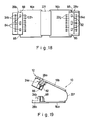
connector housing 28 is constituted by vertically coupling two split, i.e., upper and lowerconnector housing halves connector housing half 28a is fixed to the lower surface of a one-end portion of anupper circuit board 16b by screws (not shown), and the lowerconnector housing half 28b is fixed to the upper surface of a one-end portion of alower circuit board 16a by screws (not shown). - As shown in Fig. 17, the upper
connector housing half 28a is formed to have a size larger than the lowerconnector housing half 28b. Arecess 80 for receiving the lowerconnector housing half 28b from below is formed in the lower surface of the upperconnector housing half 28a. - A plurality of downwardly projecting
bosses 82 are formed on a surface for defining the upper bottom surface of therecess 80. A plurality ofrecesses 84 for complementarily receiving thesebosses 82 are formed in the upper surface of the lowerconnector housing half 28b. Upon engagement of thesebosses 82 and therecesses 84, a state wherein the upper and lowerconnector housing halves connector housing 28 is formed can be precisely defined. -
Vertical guide grooves 86 are formed in the two side surfaces of therecess 80.Ridges 88 which are complementarily fitted in theguide grooves 86 are formed on two side surfaces of the lowerconnector housing half 28b. Upon engagement of theseguide grooves 86 and theridges 88, a relative position between theconnector housing halves bosses 82 and therecesses 84. After assembly, parallelness between the twocircuit boards - Mounting
holes pins connector housing halves connector housing halves pins holes connector housing halves - Assembly of the
connector housing halves - As has been described above with reference to Figs. 4A and 4B, upper and lower edges X and Y are cut off from the
common circuit board 22 on whichpredetermined circuit elements 22d are mounted, thus forming thecircuit boards connector housing halves open circuit boards - As described above, the corresponding connecting
pins connector housing halves pins terminals circuit boards terminals circuit boards - Thereafter, as shown in Fig. 19, the
circuit board 16a which is to be located at a lower position is held in position, and thecircuit board 16b to be located at an upper position is lifted up and moved to be parallel to thelower circuit board 16a thereabove. As shown in Fig. 17, theridges 88 are fitted in theguide grooves 86 to be guided along them, and theupper circuit board 16b is then pushed down. In this manner, the lowerconnector housing half 28b is fitted in therecess 80 of the upperconnector housing half 28a. As a result, when the fitting operation is completed, the upper and lower housing halves are integrated upon fitting of thebosses 82 and therecesses 84. - When one
connector housing 28 is formed after both theconnector housing halves circuit boards side plate 18 is attached, and aframe 20 is fitted, thus forming theIC 10 integrally with themale connector 12, as shown in Fig. 1. - As described above, in the connector structure of the fifth embodiment, the
connector housing 28 of themale connector 12 is formed by the two splitconnector housing halves IC 10 is constituted, theconnector housing halves corresponding circuit boards pins terminals IC 10 can be provided. - In the fifth embodiment, the
connector housing 28 is split into halves to maintain the good assembly property. However, the present invention is not limited to this arrangement. For example, amale connector 12 may be split into one set of connectingpins 24a and aconnector housing 28 to which the other set of connectingpins 24b are mounted in advance, as shown in Fig. 20 showing the sixth embodiment. - The sixth embodiment of the present invention will now be described with reference to Fig. 20.
- As shown in Fig. 20, in the connector structure of the sixth embodiment, the
male connector 12 comprises an integrally formedconnector housing 28 unlike in the fifth embodiment wherein theconnector 12 comprises the two splitconnector housing halves connector housing 28 has the same shape as an integrated shape of theconnector housing halves holes pins housing 28 to be aligned in two arrays. The connecting pins 24b are mounted in advance in the lower connectingholes 90b of theconnector housing 28. - More specifically, in the sixth embodiment shown in Fig. 6, the
male connector 12 is split into two sections, i.e., one set of connectingpins 24a and theconnector housing 28 to which the other set of the connectingpins 24b are mounted in advance. - Upon assembly of the
IC 10 while assembling themale connector 12 to theIC 10, twocircuit boards pins 24a are connected to connectingterminals 22h of thecircuit board 16b to be located at an upper position. Theconnector housing 28 to which the other set of connectingpins 24b are mounted in advance is fixed to thecircuit board 16a to be located at a lower position, and the other set of connectingpins 24b are connected to connectingterminals 22g of thecircuit board 16a. - Thereafter, like in the fifth embodiment, one
circuit board 16a is held in position, and theother circuit board 16b is lifted up and moved to be parallel to thelower circuit board 16a thereabove. One set of connectingpins 24a connected to theother circuit board 16b are inserted in and fixed to the mountingholes 90a formed in theconnector housing 28 fixed to onecircuit board 16a. - In a state wherein the arrays of the connecting
pins connector housing 28, theconnector housing 28 and theupper circuit board 16a are fixed to each other. - In this manner, when the
connector housing 28 is fixed to thecircuit boards circuit boards side plate 18 is attached, and aframe 20 is fitted like in the fifth embodiment, thus forming theIC 10 integrally with themale connector 12 shown in Fig. 1. - As described above, in the connector structure of the sixth embodiment, the
connector housing 28 of themale connector 12 is formed with the other set of connectingpins 24b mounted in advance, and one set of connectingpins 24a are mounted to be connected to the connectingterminals 22h of theother circuit board 16b. Before theIC 10 is assembled, after one set of connectingpins 24a are mounted on theconnector housing 28, theother circuit board 16b is fixed to the connector housing. - In the sixth embodiment, a good assembly property of the
IC 10 can be maintained. - As many apparently widely different embodiments of the present invention can be made without departing from the spirit and scope thereof, it is to be understood that the invention is not limited to the specific embodiments thereof except as defined in the appended claims.
Claims (28)
a pair of circuit boards (16a; 16b), each of said circuit boards including:
a metal circuit board main body (22a); an insulating layer (22b) formed on an entire surface of said circuit board main body (22a); a conductive layer (22c) formed on said insulating layer (22b) in a predetermined circuit pattern; and a plurality of circuit elements (22d) electrically connected to a predetermined portion of said conductive layer (22c); and
externally connecting connector means (12) electrically connected to another connector (14),
characterized in that:
said externally connecting connector means (12) comprises:
a connector housing (28 or 28′) fixed to said pair of circuit boards (16a; 16b) and having a recess (30) for receiving said another connector (14), a plurality of through holes (28b; 28c; 28f′; 28g′) being formed in said connector housing (28 or 28′); and
a plurality of connector pins (24a; 24b), one-end portions of which are connected to connecting terminals (22g; 22h) formed at an edge portion of said conductive layer (22c), middle portions of which extend through the through holes (28b; 28c or 28f′; 28g′) formed in said connector housing (28 or 28′), and the other-end portions of which project into said recess (30).
characterized in that
said connector housing (28) is of an internal mounting type, which is fixed while being fitted between said pair of circuit boards (16a; 16b).
characterized in that
said connector housing (28) comprises said recess (30) which is open to a side surface at the same side as the side of said circuit board to which said connector housing (28) is fixed, and
the through holes include a plurality of pairs of upper and lower through holes (28b; 28c) which are formed along a widthwise direction in a main body (28a) portion defining a bottom surface of said recess (30).
characterized in that
said connecting terminals (22g; 22h) are aligned in an array along the widthwise direction on one circuit board (16a),
the connector pins (24a) inserted through the upper through holes (28b) are electrically connected to every other connecting terminals (22g), and
the connector pins (24b) inserted through the lower through holes (28c) are electrically connected to the remaining connecting terminals (22h).
characterized in that
each of said connector pins (24a; 24b) is fixed to the corresponding connecting terminal (22g; 22h) by soldering to be electrically connected thereto.
characterized in that
each of the connector pins (24b) inserted through the lower through holes (28c) comprises an arch portion (32) in a portion located between said connector housing (28) and said one circuit board (16a).
characterized in that
said connecting terminals (22g; 22h) are aligned in front and rear arrays along the widthwise direction on one circuit board (16a),
the connector pins (24a) inserted through the upper through holes (28b) are electrically connected to the rear connecting terminals (22g), and
the connector pins (24b) inserted through the lower through holes (28c) are electrically connected to the front connecting terminals (22h).
characterized in that
each of the connector pins (24b) inserted through the lower through holes (28c) comprises an arch portion (32) in a portion located between said connector housing (28) and said one circuit board (16a).
characterized in that
each of said connector pins (24a; 24b) is fixed to the corresponding connecting terminal (22g; 22h) by soldering to be electrically connected thereto.
characterized in that
a one-end portion of each of said connector pins (24a; 24b) is electrically connected to a corresponding connecting terminal (22g; 22h) through a bonding wire (34), and a middle portion thereof is fixed in the corresponding through hole (28b; 28c).
characterized in that
each group of said connecting terminals (21g; 22h) are aligned in an array along the widthwise direction on each of said pair of circuit boards (16b; 16a),
the connector pins (24a) inserted through the upper through holes (28b) are electrically connected to the connecting terminals (22g) aligned on the upper circuit board (16b), and
the connector pins (24b) inserted through the lower through holes (28c) are electrically connected to the connecting terminals (22h) aligned on the lower circuit board (16a).
characterized in that
the upper through holes (28b) are formed at a substantially central portion of said connector housing (28), and
each of the connector pins (24b) inserted through the lower through holes (28c) comprises an arch portion (32) in a portion located between said connector housing (28) and the lower circuit board (16a).
characterized in that
said connector housing (28′) is of an external mounting type housing which is fixed to outer surfaces of said pair of circuit boards (16a; 16b).
characterized in that
said connector housing (28′) integrally comprises a main body portion (28a′) for closing an opening end portion of said circuit boards (16a; 16b), a pair of mounting portions (28d′; 28e′) extending from said main body portion (28a′) toward the corresponding circuit boards (16a; 16b) and mounted on the outer surfaces of the corresponding circuit boards (16a; 16b), and a pair of connecting portions (28b′; 28c′), extending from said main body portion (28a′) in directions opposite to the extending directions of said mounting portions (28d′; 28e′), for defining said recess (30) therebetween.
characterized in that
each of said pair of circuit boards (16a; 16b) integrally comprises a bent portion (22i; 22j) bent outwardly on a mounting side of said connector housing (28′), and
said connector housing (28′) integrally comprises a main body portion (28a) for closing an opening end portion of said circuit boards (16a; 16b), a pair of mounting portions (28d′; 28e′) extending from said main body portion (28a′) toward the corresponding bent portions (22i; 22j) and mounted on end faces of the corresponding circuit boards (16a; 16b), and a pair of connecting portions (28b′; 28c′), extending from said main body portion (28a′) in directions opposite to the extending directions of said mounting portions (28d′; 28e′), for defining said recess (30) therebetween.
characterized in that
the through holes include a plurality of pairs of upper and lower through holes (28f′; 28g′) which are formed along a widthwise direction in said main body portion (28a′) defining a bottom surface of said recess (30).
characterized in that
each group of said connecting terminals (22g; 22h) are aligned in an array along the widthwise direction on each of said pair of circuit boards (16b; 16a),
the connector pins (24a) inserted through the upper through holes (28f′) are electrically connected to the connecting terminals (22g) aligned on the upper circuit board (16b), and
the connector pins (24b) inserted through the lower through holes (22g′) are electrically connected to the connecting terminals (22h) aligned on the lower circuit board (16a).
characterized in that
each of said connector pins (24a; 24b) has a stepped portion in a middle portion thereof, and is soldered to the corresponding connecting terminal (22g; 22h) while one-end portion thereof is folded back at 180°.
characterized in that
said connector housing (28) includes:
a pair of connector housing halves (28a; 28b) respectively fixed to said pair of circuit boards (16b; 16a) before said pair of circuit boards (16a; 16b) are assembled to oppose each other, and having a plurality of connector pins (24a; 24b) connected to the corresponding conductive layers (22c); and
superposition means (82, 86; 84, 88) which are respectively formed on said connector housing halves (28a; 28b) and are superposed on each other so as to constitute one connector housing (28) when said pair of circuit boards (16a; 16b) are assembled to oppose each other.
characterized in that
said superposition means includes:
at least one projection (82) formed on a contact surface of one connector housing half (28a) with respect to the other connector housing half (28b); and
at least one recess (84), formed on a contact surface of the other connector housing half (28b) with respect to one connector housing half (28a), for complementarily receiving said each projection (82).
characterized in that
said superposition means includes:
a recess (80), formed on a surface of one connector housing half (28a) facing the other connector housing (28b), for receiving said other connector housing half (28b) as a whole;
engaging portions (86) formed on two side surfaces of said recess (80); and
engaged portions (88) formed on two side surfaces of said other connector housing half (28b) and complementarily engaged with said engaging portions (86).
characterized in that
said engaging portions (86) comprise engaging grooves extending in an engaging direction, and
said engaged portions (88) comprise ridges complementarily fitted in said engaging grooves (86).
characterized in that
said connector housing (28) is fixed in advance on one circuit board (16a) before said pair of circuit boards (16a; 16b) are assembled to oppose each other, said connector pins (24a; 24b) include first connector pins (24b) mounted in advance in said connector housing (26) to be inserted thereto before the assembly, and second connector pins (24a) electrically and mechanically connected in advance to connecting terminals formed at an edge portion of said conductive layer of the other circuit board (16b), and
said externally connecting connector means (12) further includes a mounting portion (90a) which is formed on said connector housing (28) and to which said second connector pins (24a) are mounted when said pair of circuit boards are assembled to oppose each other.
characterized in that
said mounting portion comprises through holes (90a) through which said second connector pins (24a) are inserted so that the other-end portions thereof project into said recess (30).
a pair of circuit boards (16a; 16b), each of said circuit boards (16a; 16b) including:
a metal circuit board main body (22a); an insulating layer (22b) formed on an entire surface of said circuit board main body (22a); a conductive layer (22c) formed on said insulating layer (22b) in a predetermined circuit pattern; and a plurality of circuit elements (22d) electrically connected to a predetermined portion of said conductive layer (22c); and
externally connecting connector means (12) electrically connected to another connector (14),
characterized in that:
a plurality of integrated circuits (44; 46) are formed to have independent control functions, and
characterized by further comprising:
a connecting box (40) to which said plurality of integrated circuits (44; 46) are simultaneously mounted through the corresponding externally connecting connector means (48a; 50a) to be electrically connected thereto; and
multiplex transmission means (56; 70), arranged in said connecting box (40), for connecting said plurality of integrated circuits (44; 46) and portions to be controlled through multiplex transmission.
characterized in that
each of said integrated circuits (44; 46) comprises a multiplex interface circuit (44b; 46b) constituted by a predetermined group out of said circuit elements (22d).
characterized in that
said externally connecting connector means (48a; 50a) comprises four connector pins corresponding to four multiplex terminals for a power supply, two bus lines, and ground.
a pair of circuit boards (16a; 16b), each of said circuit boards (16a; 16b) including:
a metal circuit board main body (22a); an insulating layer (22b) formed on an entire surface of said circuit board main body (22a); a conductive layer (22c) formed on said insulating layer (22b) in a predetermined circuit pattern; and a plurality of circuit elements (22d) electrically connected to a predetermined portion of said conductive layer (22c); and
externally connecting connector means (12) electrically connected to another connector (14), characterized in that:
one functional component for a vehicle is constituted by an independent integrated circuit, and
said circuit board main body (22a) of said circuit board (16a; 16b) is defined as a functional component case.
Applications Claiming Priority (8)
| Application Number | Priority Date | Filing Date | Title |
|---|---|---|---|
| JP26944788 | 1988-10-27 | ||
| JP269447/88 | 1988-10-27 | ||
| JP273301/88 | 1988-10-31 | ||
| JP27330188A JP2621960B2 (en) | 1988-10-31 | 1988-10-31 | Mounting device for integrated circuit having metal substrate |
| JP323744/88 | 1988-12-23 | ||
| JP63323744A JP2746965B2 (en) | 1988-12-23 | 1988-12-23 | Connector structure of integrated circuit having metal substrate |
| JP1228279A JP2808546B2 (en) | 1988-10-27 | 1989-09-05 | Automotive integrated circuits |
| JP228279/89 | 1989-09-05 |
Publications (2)
| Publication Number | Publication Date |
|---|---|
| EP0366141A1 true EP0366141A1 (en) | 1990-05-02 |
| EP0366141B1 EP0366141B1 (en) | 1995-10-18 |
Family
ID=27477320
Family Applications (1)
| Application Number | Title | Priority Date | Filing Date |
|---|---|---|---|
| EP19890119996 Expired - Lifetime EP0366141B1 (en) | 1988-10-27 | 1989-10-27 | Integrated circuit for vehicle |
Country Status (2)
| Country | Link |
|---|---|
| EP (1) | EP0366141B1 (en) |
| DE (1) | DE68924576T2 (en) |
Cited By (8)
| Publication number | Priority date | Publication date | Assignee | Title |
|---|---|---|---|---|
| EP0374833A2 (en) * | 1988-12-23 | 1990-06-27 | Sanyo Electric Co., Ltd. | Connector structure for hybrid integrated circuit |
| FR2671935A1 (en) * | 1991-01-22 | 1992-07-24 | Peugeot | Box for a power electronic circuit |
| DE4106453C1 (en) * | 1991-02-28 | 1992-08-06 | Siemens Ag, 8000 Muenchen, De | |
| EP0552042A1 (en) * | 1992-01-16 | 1993-07-21 | Mitsubishi Denki Kabushiki Kaisha | Portable semiconductor storage apparatus |
| EP0557883A1 (en) * | 1992-02-24 | 1993-09-01 | Motorola, Inc. | Laminated electronic module assembly |
| EP1152649A2 (en) * | 2000-05-03 | 2001-11-07 | Deere & Company | Electronic controller unit and method of manufacturing |
| EP1463104A2 (en) * | 2003-03-28 | 2004-09-29 | Delphi Technologies, Inc. | Overmolded electronic package including circuit-carrying substrate |
| CN105555072A (en) * | 2016-02-17 | 2016-05-04 | 珠海格力电器股份有限公司 | Electrical box and air conditioner with same |
Citations (4)
| Publication number | Priority date | Publication date | Assignee | Title |
|---|---|---|---|---|
| DE3228398A1 (en) * | 1982-07-29 | 1984-02-02 | Siemens AG, 1000 Berlin und 8000 München | RF-sealed plug-in assembly |
| DE3345701A1 (en) * | 1983-12-17 | 1985-06-27 | Robert Bosch Gmbh, 7000 Stuttgart | Electrical switching apparatus having an end connecting plate which supports plug parts |
| DE8430486U1 (en) * | 1984-10-17 | 1988-12-08 | Robert Bosch Gmbh, 7000 Stuttgart, De | |
| US4858071A (en) * | 1987-02-24 | 1989-08-15 | Nissan Motor Co., Ltd. | Electronic circuit apparatus |
-
1989
- 1989-10-27 DE DE1989624576 patent/DE68924576T2/en not_active Expired - Fee Related
- 1989-10-27 EP EP19890119996 patent/EP0366141B1/en not_active Expired - Lifetime
Patent Citations (4)
| Publication number | Priority date | Publication date | Assignee | Title |
|---|---|---|---|---|
| DE3228398A1 (en) * | 1982-07-29 | 1984-02-02 | Siemens AG, 1000 Berlin und 8000 München | RF-sealed plug-in assembly |
| DE3345701A1 (en) * | 1983-12-17 | 1985-06-27 | Robert Bosch Gmbh, 7000 Stuttgart | Electrical switching apparatus having an end connecting plate which supports plug parts |
| DE8430486U1 (en) * | 1984-10-17 | 1988-12-08 | Robert Bosch Gmbh, 7000 Stuttgart, De | |
| US4858071A (en) * | 1987-02-24 | 1989-08-15 | Nissan Motor Co., Ltd. | Electronic circuit apparatus |
Cited By (13)
| Publication number | Priority date | Publication date | Assignee | Title |
|---|---|---|---|---|
| EP0374833A3 (en) * | 1988-12-23 | 1991-02-06 | Sanyo Electric Co., Ltd. | Connector structure for hybrid integrated circuit |
| US5040994A (en) * | 1988-12-23 | 1991-08-20 | Sanyo Electric Co., Ltd. | Connector structure for hybrid integrated circuit |
| EP0374833A2 (en) * | 1988-12-23 | 1990-06-27 | Sanyo Electric Co., Ltd. | Connector structure for hybrid integrated circuit |
| FR2671935A1 (en) * | 1991-01-22 | 1992-07-24 | Peugeot | Box for a power electronic circuit |
| DE4106453C1 (en) * | 1991-02-28 | 1992-08-06 | Siemens Ag, 8000 Muenchen, De | |
| US5331516A (en) * | 1992-01-16 | 1994-07-19 | Mitsubishi Denki Kabushiki Kaisha | Portable semiconductor apparatus |
| EP0552042A1 (en) * | 1992-01-16 | 1993-07-21 | Mitsubishi Denki Kabushiki Kaisha | Portable semiconductor storage apparatus |
| EP0557883A1 (en) * | 1992-02-24 | 1993-09-01 | Motorola, Inc. | Laminated electronic module assembly |
| EP1152649A2 (en) * | 2000-05-03 | 2001-11-07 | Deere & Company | Electronic controller unit and method of manufacturing |
| EP1152649A3 (en) * | 2000-05-03 | 2004-01-02 | Deere & Company | Electronic controller unit and method of manufacturing |
| EP1463104A2 (en) * | 2003-03-28 | 2004-09-29 | Delphi Technologies, Inc. | Overmolded electronic package including circuit-carrying substrate |
| EP1463104A3 (en) * | 2003-03-28 | 2011-05-18 | Delphi Technologies, Inc. | Overmolded electronic package including circuit-carrying substrate |
| CN105555072A (en) * | 2016-02-17 | 2016-05-04 | 珠海格力电器股份有限公司 | Electrical box and air conditioner with same |
Also Published As
| Publication number | Publication date |
|---|---|
| EP0366141B1 (en) | 1995-10-18 |
| DE68924576T2 (en) | 1996-04-18 |
| DE68924576D1 (en) | 1995-11-23 |
Similar Documents
| Publication | Publication Date | Title |
|---|---|---|
| US6099324A (en) | Electrical motor unit having a control module | |
| US7167377B2 (en) | Circuit-constituting unit and method of producing the same | |
| JP2690533B2 (en) | Connector structure of hybrid integrated circuit | |
| US6291770B1 (en) | Wiring system and method therefor | |
| CN1050810C (en) | Hybrid junction box | |
| US5134546A (en) | Vehicle control unit structure | |
| EP0502377B1 (en) | Filter connector | |
| JPS6261856A (en) | Wiring device assembled with functions for automobile | |
| KR19990082019A (en) | Vehicle control device | |
| US5283712A (en) | Integrated circuit for vehicle | |
| EP2034809B1 (en) | Electronic device including printed circuit board and electronic element mounted on the printed circuit board | |
| US20030090358A1 (en) | Power distributing box and power-device module | |
| KR101520990B1 (en) | Electrical connector | |
| EP0366141B1 (en) | Integrated circuit for vehicle | |
| EP1174311A1 (en) | Junction box | |
| US7275962B1 (en) | Connector | |
| EP1577977A1 (en) | Electrical junction box | |
| KR930011604B1 (en) | Integrated circuit for vehicle | |
| JPH02170598A (en) | On-vehicle control unit structure | |
| JP2746965B2 (en) | Connector structure of integrated circuit having metal substrate | |
| KR20010024914A (en) | Electronic control device | |
| JP2904280B2 (en) | Connector structure of integrated circuit having metal substrate | |
| JPH02119076A (en) | Integrated circuit having metal substrate | |
| JP2621960B2 (en) | Mounting device for integrated circuit having metal substrate | |
| CN211556232U (en) | Socket connector |
Legal Events
| Date | Code | Title | Description |
|---|---|---|---|
| PUAI | Public reference made under article 153(3) epc to a published international application that has entered the european phase |
Free format text: ORIGINAL CODE: 0009012 |
|
| AK | Designated contracting states |
Kind code of ref document: A1 Designated state(s): DE FR GB |
|
| 17P | Request for examination filed |
Effective date: 19901023 |
|
| 17Q | First examination report despatched |
Effective date: 19920617 |
|
| GRAA | (expected) grant |
Free format text: ORIGINAL CODE: 0009210 |
|
| AK | Designated contracting states |
Kind code of ref document: B1 Designated state(s): DE FR GB |
|
| REF | Corresponds to: |
Ref document number: 68924576 Country of ref document: DE Date of ref document: 19951123 |
|
| ET | Fr: translation filed | ||
| PLBE | No opposition filed within time limit |
Free format text: ORIGINAL CODE: 0009261 |
|
| STAA | Information on the status of an ep patent application or granted ep patent |
Free format text: STATUS: NO OPPOSITION FILED WITHIN TIME LIMIT |
|
| 26N | No opposition filed | ||
| PGFP | Annual fee paid to national office [announced via postgrant information from national office to epo] |
Ref country code: FR Payment date: 20001010 Year of fee payment: 12 |
|
| PGFP | Annual fee paid to national office [announced via postgrant information from national office to epo] |
Ref country code: DE Payment date: 20001023 Year of fee payment: 12 |
|
| PGFP | Annual fee paid to national office [announced via postgrant information from national office to epo] |
Ref country code: GB Payment date: 20001025 Year of fee payment: 12 |
|
| PG25 | Lapsed in a contracting state [announced via postgrant information from national office to epo] |
Ref country code: GB Free format text: LAPSE BECAUSE OF NON-PAYMENT OF DUE FEES Effective date: 20011027 |
|
| REG | Reference to a national code |
Ref country code: GB Ref legal event code: IF02 |
|
| GBPC | Gb: european patent ceased through non-payment of renewal fee |
Effective date: 20011027 |
|
| PG25 | Lapsed in a contracting state [announced via postgrant information from national office to epo] |
Ref country code: FR Free format text: LAPSE BECAUSE OF NON-PAYMENT OF DUE FEES Effective date: 20020628 |
|
| PG25 | Lapsed in a contracting state [announced via postgrant information from national office to epo] |
Ref country code: DE Free format text: LAPSE BECAUSE OF NON-PAYMENT OF DUE FEES Effective date: 20020702 |
|
| REG | Reference to a national code |
Ref country code: FR Ref legal event code: ST |