EP0362723A2 - Réseau pour système de commutation - Google Patents
Réseau pour système de commutation Download PDFInfo
- Publication number
- EP0362723A2 EP0362723A2 EP89118134A EP89118134A EP0362723A2 EP 0362723 A2 EP0362723 A2 EP 0362723A2 EP 89118134 A EP89118134 A EP 89118134A EP 89118134 A EP89118134 A EP 89118134A EP 0362723 A2 EP0362723 A2 EP 0362723A2
- Authority
- EP
- European Patent Office
- Prior art keywords
- buffer
- circuit
- input
- flip
- memory
- Prior art date
- Legal status (The legal status is an assumption and is not a legal conclusion. Google has not performed a legal analysis and makes no representation as to the accuracy of the status listed.)
- Granted
Links
Images

Classifications
-
- H—ELECTRICITY
- H04—ELECTRIC COMMUNICATION TECHNIQUE
- H04L—TRANSMISSION OF DIGITAL INFORMATION, e.g. TELEGRAPHIC COMMUNICATION
- H04L49/00—Packet switching elements
- H04L49/30—Peripheral units, e.g. input or output ports
- H04L49/3018—Input queuing
-
- H—ELECTRICITY
- H04—ELECTRIC COMMUNICATION TECHNIQUE
- H04L—TRANSMISSION OF DIGITAL INFORMATION, e.g. TELEGRAPHIC COMMUNICATION
- H04L49/00—Packet switching elements
- H04L49/25—Routing or path finding in a switch fabric
- H04L49/253—Routing or path finding in a switch fabric using establishment or release of connections between ports
- H04L49/254—Centralised controller, i.e. arbitration or scheduling
-
- H—ELECTRICITY
- H04—ELECTRIC COMMUNICATION TECHNIQUE
- H04L—TRANSMISSION OF DIGITAL INFORMATION, e.g. TELEGRAPHIC COMMUNICATION
- H04L49/00—Packet switching elements
- H04L49/40—Constructional details, e.g. power supply, mechanical construction or backplane
Definitions
- the invention relates to a switching matrix for a switching system which is constructed in the manner of a space division switching matrix with m / 1 stages with feeder lines and one customer line each and in which cells are transmitted using a time division method and on the basis of the routing information contained in the cell header the switching of the cells takes place and in which, if the routing information and the address of the customer line match, the cell arriving on the supply line is read into the buffer memory assigned to this customer line and a decision circuit is provided.
- the switching matrix is particularly suitable for use in asynchronous time multiple processes.
- the proportion of data traffic to be transmitted is constantly increasing in communication networks.
- switching systems for data and telephone traffic were set up separately. Since the data rate of the data signals to be transmitted can take on a multitude of different values, it is difficult to combine data and telephone switching in one network node.
- the cells can have the same or different lengths. They consist of useful and address information, the address information being accommodated in a header or cell header.
- the number of bits in a cell is referred to as its length, with values between 120 and 256 bits for the useful information and 32 or 16 bits for the cell header being provided for this purpose in the standardization proposals.
- the time intervals in which cells are transmitted are referred to as frames. A frame can contain a valid cell or be empty.
- the switching nodes can be centrally buffered systems (as known for example from the European patent application with the publication number 0 183 592) or decentrally buffered systems.
- centrally buffered systems there is only one buffer in which each incoming line stores its incoming cells and from which each outgoing line reads the cells destined for it.
- Sy Systems with decentralized buffering are differentiated according to whether cells are buffered exclusively on the input side or whether the buffers are arranged exclusively in front of the outgoing lines or whether they are systems with input and output buffering. This is also known as switching matrix buffering if a buffer is assigned to each switching point of a switching matrix.
- each feeder line of an m / 1 level is assigned its own evaluation logic.
- Each feeder line is connected to a buffer memory, which receives and stores the cells supplied via the feeder line, provided a comparator assigned to the buffer memory has determined that the address of the customer line stored in an address memory matches the routing information contained in the cell header.
- cells which are intended for the customer line of this stage arrive at several feeder lines of an m / 1 stage at the same time, these cells can also be forwarded to the buffer stores at the same time. From these, however, they can only be read out one after the other onto the customer line.
- a decision circuit is assigned to each m / 1 stage, which determines the sequence of the feeder lines to be switched through. The order is determined by the spatial arrangement of the feeder lines. If several cells arrive at a feed line of an m / 1 stage, the destined for the customer line of this level and stored in the form of a queue in the buffer memory, this is also taken into account.
- the invention has for its object to improve a switching matrix of the type mentioned in such a way that the queues formed in the buffer memories of the m / 1 levels are processed as fairly as possible. This means that cells destined for the same customer line, which arrive one after the other in an m / 1 stage, leave them in the same order in which they arrived.
- the m / 1 stages S are designed such that cells arriving at the feeder lines Z1 ... Zn at the same time or almost simultaneously, which cells are intended, for example, for the customer line A1 according to their routing information, are initially stored in the buffer store P immediately after their arrival. They must then be read out successively onto the subscriber line A1 from this buffer memory.
- FIG. 2 shows an embodiment of an m / 1 stage S.
- m feeder lines Z1... Zm can be connected to the m / 1 stage.
- the cells arriving on them can be forwarded to a customer line A.
- a comparator C and a buffer store B are connected to each feeder line Z1 ... Zm.
- These buffer stores B in their entirety form the buffer store P shown schematically in FIG. 1.
- the outputs of the buffer stores B are all connected to the consumer line A of this m / 1 Stage connected.
- the clock circuit T is used to generate the clock signals necessary for timing the m / 1 stage from an input clock C1. These are the cell start signal BS, the cell burst signal BB and the series switching signal Ai.
- the clock signals cell start signal BS and cell burst signal BB control the reading of the cells into the buffer memory B.
- an address memory L is connected, which contains the address of the associated customer line A.
- the bit pattern contained in the address memories L which characterizes the address of the customer line A is the same for all comparators of this m / 1 level.
- a control logic circuit is connected to the buffer memory B.
- This has a first flip-flop FF1 and a first AND gate U1.
- the set input of the flip-flop FF1 is connected to the output of the comparator C, the clock input of the flip-flop FF1 is supplied with the cell start signal BS.
- the non-inverting output of the flip-flop FF1 is connected to the input of a memory FIFO, which can be read into a buffer FF3.
- this buffer is designed as a flip-flop with a non-inverting output and with a clock input.
- the output of the buffer store FF3 is connected to the decision circuit CA.
- the output of the flip-flop FF1 is connected to a first input of the first AND gate U1, to the second input of which the cell burst signal BB is applied.
- the output of the first AND gate U1 is connected to the write-in control input of the input buffer B.
- the control logic circuit also contains a second flip-flop FF2 and a second AND gate U2.
- the cell burst signal BB is likewise fed to the first input of the AND gate U2, while the clock input of the flip-flop FF2 is fed the cell start signal BS.
- the non-inverting output of the second flip-flop FF2 is connected to the second input of the AND gate U2, the output of which is connected to the input of the buffer memory B, via which the reading out of the buffer memory can be triggered (read control input).
- the inverting output of the flip-flop FF2 is connected to an input of the buffer memory B, via which the readout of the buffer memory can be prevented when the OE signal is applied (read lock input).
- the flip-flop FF1 is also connected on the output side to a multiple-OR circuit OS, on the input side of which the flip-flops FF1 of the remaining Zu Bringer effet Z1 ... Zm associated logic circuits are connected.
- the multiple OR circuit OS is connected to a first input of a third AND circuit U3, the second input of which is supplied with the cell start signal BS.
- the output of the AND circuit U3 is connected to the clock input of the memory FIFO, to the readout control input of which the output of a fourth AND circuit U4 is connected.
- This AND circuit U4 is supplied with the cell start signal BS at a first input and a series switching signal Ae at a second input, which is delayed and inverted in the decision circuit CA from the series switching signal Ai generated in the clock circuit T and supplied with it.
- the cell start signal BS is also fed to the clock input of the buffer store FF3.
- each comparator C continuously compares the data arriving on the associated feeder line with the address stored in the memory L for the customer line A. Synchronized with the cell start signal BS when the routing information occurs, the result is stored in the first flip-flop FF1. If the routing information corresponds to the address of the customer line A, the characteristic AND state then present at the non-inverting output of the first flip-flop FF1 opens the first AND gate U1, to which the cell burst signal BB is simultaneously applied. This generates the write-in signal SI, which causes the data arriving on the feeder line to be written into the buffer memory B.
- a logical 1 is entered in the FIFO memory.
- the function of the multiple OR circuit OS is that for each of the Zubrin lines Z1 ... Zm, on which no cell has arrived, a logical 0 is entered in the memory FIFO, provided that a cell has arrived on any feeder line and thus at least one logical FIFO in the memory FIFO of the m / 1 level 1 has been entered.
- the characteristic state of the corresponding flip-flop 1 had reached all AND circuits U3 via the multiple-OR circuit and, as the output signal thereof, had reached the clock input of all memories FIFO and had the effect that the respective one at the output of the corresponding first flip-flop Flops FF1 pending characteristic state was written into the memory FIFO.
- the sequence of events on the respective feeder lines is stored in the respective memory FIFO. The only exceptions are those intervals in which a cell did not arrive on any feeder line because then no signal reached the clock input of the memory FIFO.
- the decision circuit CA cyclically allocates the output lines A to the feeder lines, for which a 1 is stored in the respective buffer store FF3. If such a cycle has ended, the next position is read out of all memories FIFO and the result is stored in the respective buffers FF3.
- the end of a cycle of the decision circuit CA is indicated by the change in the series switching signal Ae emitted by the decision circuit CA from "LOW" to "HIGH” at an output of the decision circuit CA. This series switching signal Ae is present at the second inputs of the AND circuits U4.
- a positive decision at an output of the decision circuit CA is stored in the corresponding flip-flop FF2.
- the associated AND gate U2 is opened with simultaneous application of the cell burst signal BB and the output signal SO causes the content of the buffer memory B to be read onto the consumer line A.
- the buffer memories of the other logic circuits on the further feeder lines are via the signal OE blocked at the outputs of the respective flip-flops FF2.
- the size of the FIFO memory which stores the information "cell arrival / no cell arrival", is limited by the length of the queue. However, this quantity cannot be justified in terms of circuitry, but is determined solely by the statistical properties of the arrival processes. The dimensioning therefore results from the knowledge or estimation of the traffic behavior of the sources and the application of known formulas of queue theory.
- the decision circuit CA therefore works with the characteristic states of the buffer stores FF3.
- the assignment of the customer line A takes place depending on the respective characteristic state.
- a signal at the output of the buffer store FF3, which indicates that its characteristic state is zero, is not particularly evaluated.
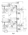
- FIG. 3 An embodiment of a decision circuit CA for a 16/1 stage for sixteen feeder lines is shown in FIG. 3.
- Such a decision circuit CA is composed of individual logic circuits LCA of the same structure, such a logic circuit being connected to the output of each of the intermediate memories FF3 of the arrangement shown in FIG. 2.
- the logic circuit assigned to the buffer store FF31 has an edge-triggered D flip-flop DFF1, at the D input of which the output of an AND gate UCA1 is indicated is closed, with the output of the intermediate buffer FF31 being connected to the first input of this AND gate UCA1.
- the inverting output of this D flip-flop DFF1 is connected to a NOR gate NOR1 and the non-inverting output of this D flip-flop DFF1 is connected to an OR gateOCA1.
- the outputs of the NOR gates form the outputs ACA1, ACA2 ... of the decision circuit CA and are connected to corresponding inputs of the control logic circuits of the buffer memory B of the circuit arrangement shown in FIG. 2. Since the clock inputs of the D flip-flops DFF2 ... DFF16 are each connected via an OR gate to the non-inverting output of the preceding D flip-flops DFF1 ... DFF15, the individual D flip-flops can be considered as in Series can be viewed horizontally.
- a series switching signal Ai generated in the clock circuit T is present at a first clock input of the decision circuit CA.
- a positive edge of Ai is generated after the result of comparator C, which is first in the FIFO memories, has been transferred to the buffer memories FF3 (FF31 ... FF316).
- the signal Ai is fed in the decision circuit CA to an input of all OR gates OCA1 to OCA 16 and also to the clock input of the first D flip-flop DFF1.
- the output signal emitted from an output of the OR gate OCA 16 at an output of the decision circuit CA is fed back to a further input of the decision circuit CA as a series switching signal Ae with the interposition of an inverter IN and is connected to the second inputs of the AND gates U1 ... U16 at. It can also be fed to further decision circuits in the switching system.
- the series switching signal Ai has the logic characteristic "LOW” and all D flip-flops DFF1 ... DFF16 have this logic characteristic "LOW” stored.
- a series switching signal Ae with the logical characteristic state "HIGH” is thus present at every second input of the AND gates UCA1 ... UCA16 and the AND gates are switched through when the associated counters have an output state greater than zero.
- this signal passes through the decision circuit CA with a gate delay caused by the running time in the OR circuit OCA16 and the input data are transferred to the D flip-flops DFF1 ... DFF16, so that each flip-flop, whose associated counter had the initial state greater than zero, now has the characteristic state "HIGH” at its non-inverting output.
- the series switching signal Ae goes into the logic characteristic "LOW” and all AND gates UCA1 to UCA16 are "disabled”.
- the series switching signal Ai changes to the logic characteristic "LOW".
- This negative edge runs through the chain of the OR gates up to the first D flip-flop that has stored the "HIGH” state. It causes the output signal at the inverting output of the D flip-flop to be switched through to the respective output ACA via the associated NOR gate.
- This output signal at ACA causes the second flip-flop FF2 in the circuit shown in FIG. 2 to read out the data stored in the associated buffer memory B to the customer line A.
- the D flip-flop in question locks simultaneously with the at its non-inverting output, the "HIGH” characteristic state is followed by the D flip-flops following in the series circuit, since the "HIGH” state is retained after the OR gate. After reading out the data from the activated buffer memory, a new positive edge of the series switching signal Ai is generated in the clock circuit.
- the D flip-flop which just had the identification state "HIGH” is reset and assumes the logical identification state "LOW". If the series switching signal Ai again assumes the logical characteristic state "LOW", the next buffer memory can be read out, the associated D-flip-flop of which has stored the logical characteristic state "HIGH”. The cycle described in this way continues until the last D-flip-flop of the series circuit has been reset, which had the logic characteristic "HIGH”. With the next positive edge of the series switching signal Ai, input data can then again be transferred to the D flip-flops DFF1 ... DFF16. This edge falls within the fixed grid of the positive edges of the series switching signal Ai.
Applications Claiming Priority (2)
| Application Number | Priority Date | Filing Date | Title |
|---|---|---|---|
| DE3833490A DE3833490A1 (de) | 1988-10-01 | 1988-10-01 | Koppelfeld fuer ein vermittlungssystem |
| DE3833490 | 1988-10-01 |
Publications (3)
| Publication Number | Publication Date |
|---|---|
| EP0362723A2 true EP0362723A2 (fr) | 1990-04-11 |
| EP0362723A3 EP0362723A3 (fr) | 1991-09-18 |
| EP0362723B1 EP0362723B1 (fr) | 1994-12-14 |
Family
ID=6364225
Family Applications (1)
| Application Number | Title | Priority Date | Filing Date |
|---|---|---|---|
| EP89118134A Expired - Lifetime EP0362723B1 (fr) | 1988-10-01 | 1989-09-29 | Réseau pour système de commutation |
Country Status (5)
| Country | Link |
|---|---|
| US (1) | US5067124A (fr) |
| EP (1) | EP0362723B1 (fr) |
| JP (1) | JPH02143747A (fr) |
| CA (1) | CA1325263C (fr) |
| DE (2) | DE3833490A1 (fr) |
Cited By (3)
| Publication number | Priority date | Publication date | Assignee | Title |
|---|---|---|---|---|
| EP0454218A1 (fr) * | 1990-04-21 | 1991-10-30 | Philips Patentverwaltung GmbH | Système de transmission à division temporelle |
| EP0503560A2 (fr) * | 1991-03-11 | 1992-09-16 | Fujitsu Limited | Commutateur de communication situé entre des portes d'entrée et des portes de sortie |
| WO1992019060A1 (fr) * | 1991-04-10 | 1992-10-29 | N.V. Philips' Gloeilampenfabrieken | Commutateur de cellules a faible retard et a faibles pertes en mode de transfert asynchrone |
Families Citing this family (2)
| Publication number | Priority date | Publication date | Assignee | Title |
|---|---|---|---|---|
| DE4010535A1 (de) * | 1990-04-02 | 1991-10-10 | Philips Patentverwaltung | Koppelelement fuer ein asynchrones zeitvielfachuebermittlungssystem |
| US5471623A (en) * | 1991-02-26 | 1995-11-28 | Napolitano, Jr.; Leonard M. | Lambda network having 2m-1 nodes in each of m stages with each node coupled to four other nodes for bidirectional routing of data packets between nodes |
Citations (1)
| Publication number | Priority date | Publication date | Assignee | Title |
|---|---|---|---|---|
| WO1986002510A1 (fr) * | 1984-10-18 | 1986-04-24 | Hughes Aircraft Company | PROCEDE DE TRAITEMENT ET NOEUD DE COMMUTATION NxM A FILES D'ATTENTE MULTIPLES ET A PAQUETS COMMUTES |
Family Cites Families (6)
| Publication number | Priority date | Publication date | Assignee | Title |
|---|---|---|---|---|
| FR2572871B1 (fr) * | 1984-11-08 | 1987-01-23 | Labo Cent Telecommunicat | Commutateur de paquets asynchrone |
| US4760570A (en) * | 1986-08-06 | 1988-07-26 | American Telephone & Telegraph Company, At&T Bell Laboratories | N-by-N "knockout" switch for a high-performance packet switching system |
| US4754451A (en) * | 1986-08-06 | 1988-06-28 | American Telephone And Telegraph Company, At&T Bell Laboratories | N-by-N "knockout" switch for a high-performance packet switching system with variable length packets |
| JPH01177239A (ja) * | 1988-01-06 | 1989-07-13 | Nec Corp | パケット集線装置及びパケット交換機 |
| SE462361B (sv) * | 1988-03-30 | 1990-06-11 | Ellemtel Utvecklings Ab | Paketdatavaeljare |
| DE3823878A1 (de) * | 1988-07-14 | 1990-01-18 | Philips Patentverwaltung | Koppelfeld fuer ein vermittlungssystem |
-
1988
- 1988-10-01 DE DE3833490A patent/DE3833490A1/de not_active Withdrawn
-
1989
- 1989-09-28 CA CA000614219A patent/CA1325263C/fr not_active Expired - Fee Related
- 1989-09-28 US US07/414,036 patent/US5067124A/en not_active Expired - Fee Related
- 1989-09-29 EP EP89118134A patent/EP0362723B1/fr not_active Expired - Lifetime
- 1989-09-29 DE DE58908770T patent/DE58908770D1/de not_active Expired - Fee Related
- 1989-10-02 JP JP1257633A patent/JPH02143747A/ja active Pending
Patent Citations (1)
| Publication number | Priority date | Publication date | Assignee | Title |
|---|---|---|---|---|
| WO1986002510A1 (fr) * | 1984-10-18 | 1986-04-24 | Hughes Aircraft Company | PROCEDE DE TRAITEMENT ET NOEUD DE COMMUTATION NxM A FILES D'ATTENTE MULTIPLES ET A PAQUETS COMMUTES |
Cited By (8)
| Publication number | Priority date | Publication date | Assignee | Title |
|---|---|---|---|---|
| EP0454218A1 (fr) * | 1990-04-21 | 1991-10-30 | Philips Patentverwaltung GmbH | Système de transmission à division temporelle |
| EP0503560A2 (fr) * | 1991-03-11 | 1992-09-16 | Fujitsu Limited | Commutateur de communication situé entre des portes d'entrée et des portes de sortie |
| EP0503560A3 (en) * | 1991-03-11 | 1992-12-02 | Fujitsu Limited | Switch coupled between input and output ports in communication system |
| US5303231A (en) * | 1991-03-11 | 1994-04-12 | Fujitsu Limited | Switch coupled between input and output ports in communication system |
| EP0794637A2 (fr) * | 1991-03-11 | 1997-09-10 | Fujitsu Limited | Commutateur situé entre des portes d'entrée et des portes de sortie d'un système de communication |
| EP0794637A3 (fr) * | 1991-03-11 | 1997-10-01 | Fujitsu Limited | Commutateur situé entre des portes d'entrée et des portes de sortie d'un système de communication |
| WO1992019060A1 (fr) * | 1991-04-10 | 1992-10-29 | N.V. Philips' Gloeilampenfabrieken | Commutateur de cellules a faible retard et a faibles pertes en mode de transfert asynchrone |
| US5390176A (en) * | 1991-04-10 | 1995-02-14 | U.S. Philips Corporation | Low delay or low loss switch for ATM |
Also Published As
| Publication number | Publication date |
|---|---|
| JPH02143747A (ja) | 1990-06-01 |
| DE3833490A1 (de) | 1990-04-05 |
| US5067124A (en) | 1991-11-19 |
| EP0362723B1 (fr) | 1994-12-14 |
| EP0362723A3 (fr) | 1991-09-18 |
| CA1325263C (fr) | 1993-12-14 |
| DE58908770D1 (de) | 1995-01-26 |
Similar Documents
| Publication | Publication Date | Title |
|---|---|---|
| EP0384936B1 (fr) | Procédé et dispositif pour transmettre des paquets d'information provenant de lignes d'entrée via un dispositif à communication de paquets | |
| EP0446589B1 (fr) | Commutateur ATM avec capacité de duplication | |
| EP0351014B1 (fr) | Réseau de commutation pour système de commutation | |
| DE19532422C1 (de) | Lokales, nach dem asynchronen Transfermodus (ATM) arbeitendes Netzwerk mit wenigstens zwei Ringsystemen | |
| DE4432061C1 (de) | Paketübertragungssystem | |
| EP0419959B1 (fr) | Circuit pour contrÔler le respet de débits préétablis lors de la transmission de cellules de données | |
| DE2251716C3 (de) | Verfahren zur Datenübertragung von Endstellen zu einer Zentralstation innerhalb einer Serienschleife und Schaltungsanordnungen hierzu | |
| DE2910241A1 (de) | Verfahren zur sortierung von informationen in einem uebertragungsnetz fuer numerische daten und anordnung zur durchfuehrung des verfahrens | |
| EP0289087B1 (fr) | Système de commutation par paquets | |
| EP0320772A3 (fr) | Procédé pour la commutation hybride de paquets et dispositifs à cet effet | |
| EP0329005B1 (fr) | Procédé pour l'établissement de circuits virtuels à travers les commutateurs d'un dispositif de commutation à plusieurs étages | |
| EP0682422A2 (fr) | Méthode et dispositif pour synchroniser un train de cellules transmis avec redondance | |
| DE60031519T2 (de) | Kommunikationsnetzwerk | |
| EP0362723B1 (fr) | Réseau pour système de commutation | |
| EP0322075B1 (fr) | Réseau de commutation et dispositif de commande pour un système de commutation | |
| EP0173274B1 (fr) | Méthode et montage pour la réalisation et la maintenance d'une liaison à division temporelle à large bande | |
| EP0321050B1 (fr) | Noeud de commutation d'un système de commutation à large bande | |
| EP0960551B1 (fr) | Procede et circuit pour transmettre des cellules de donnees dans le cadre de liaisons virtuelles presentant differentes priorites | |
| DE19532421C1 (de) | Lokales, nach dem asynchronen Transfermodus (ATM) arbeitendes Netzwerk zur Erzeugung von priorisierten Zellen | |
| DE19602476A1 (de) | ATM-Kommunikationsnetzeinrichtung | |
| DE19935126A1 (de) | Verfahren und Vorrichtung zur Vermittlung einer Mehrzahl von paket-orientierten Signalen | |
| EP0005489B1 (fr) | Méthode et circuit pour la transmission de données entre une station centrale et un parmi plusieurs postes de données dans un réseau de données synchrone à structure d'enveloppe | |
| DE4330295C2 (de) | Verfahren und Koppelfeldanordnung zum Übertragen von Zellen im Zuge einer Punkt-zu-Mehrpunktverbindung in einer Paketvermittlungsanlage | |
| DE3735187C2 (fr) | ||
| DE19937244B4 (de) | Verfahren zum Bestimmen von Zellenverlustprioritätsinformationen |
Legal Events
| Date | Code | Title | Description |
|---|---|---|---|
| PUAI | Public reference made under article 153(3) epc to a published international application that has entered the european phase |
Free format text: ORIGINAL CODE: 0009012 |
|
| AK | Designated contracting states |
Kind code of ref document: A2 Designated state(s): DE FR GB SE |
|
| PUAL | Search report despatched |
Free format text: ORIGINAL CODE: 0009013 |
|
| AK | Designated contracting states |
Kind code of ref document: A3 Designated state(s): DE FR GB SE |
|
| 17P | Request for examination filed |
Effective date: 19920318 |
|
| 17Q | First examination report despatched |
Effective date: 19940412 |
|
| GRAA | (expected) grant |
Free format text: ORIGINAL CODE: 0009210 |
|
| AK | Designated contracting states |
Kind code of ref document: B1 Designated state(s): DE FR GB SE |
|
| REF | Corresponds to: |
Ref document number: 58908770 Country of ref document: DE Date of ref document: 19950126 |
|
| ET | Fr: translation filed | ||
| GBT | Gb: translation of ep patent filed (gb section 77(6)(a)/1977) |
Effective date: 19950309 |
|
| REG | Reference to a national code |
Ref country code: FR Ref legal event code: CD |
|
| PGFP | Annual fee paid to national office [announced via postgrant information from national office to epo] |
Ref country code: GB Payment date: 19950831 Year of fee payment: 7 |
|
| PGFP | Annual fee paid to national office [announced via postgrant information from national office to epo] |
Ref country code: SE Payment date: 19950926 Year of fee payment: 7 |
|
| PGFP | Annual fee paid to national office [announced via postgrant information from national office to epo] |
Ref country code: FR Payment date: 19950927 Year of fee payment: 7 |
|
| PLBE | No opposition filed within time limit |
Free format text: ORIGINAL CODE: 0009261 |
|
| STAA | Information on the status of an ep patent application or granted ep patent |
Free format text: STATUS: NO OPPOSITION FILED WITHIN TIME LIMIT |
|
| PGFP | Annual fee paid to national office [announced via postgrant information from national office to epo] |
Ref country code: DE Payment date: 19951123 Year of fee payment: 7 |
|
| 26N | No opposition filed | ||
| PG25 | Lapsed in a contracting state [announced via postgrant information from national office to epo] |
Ref country code: GB Effective date: 19960929 |
|
| PG25 | Lapsed in a contracting state [announced via postgrant information from national office to epo] |
Ref country code: SE Effective date: 19960930 Ref country code: FR Effective date: 19960930 |
|
| GBPC | Gb: european patent ceased through non-payment of renewal fee |
Effective date: 19960929 |
|
| PG25 | Lapsed in a contracting state [announced via postgrant information from national office to epo] |
Ref country code: DE Effective date: 19970603 |
|
| EUG | Se: european patent has lapsed |
Ref document number: 89118134.9 |
|
| REG | Reference to a national code |
Ref country code: FR Ref legal event code: ST |
|
| REG | Reference to a national code |
Ref country code: FR Ref legal event code: ST |