EP0359567B1 - Plasma processing method and apparatus - Google Patents
Plasma processing method and apparatus Download PDFInfo
- Publication number
- EP0359567B1 EP0359567B1 EP89309352A EP89309352A EP0359567B1 EP 0359567 B1 EP0359567 B1 EP 0359567B1 EP 89309352 A EP89309352 A EP 89309352A EP 89309352 A EP89309352 A EP 89309352A EP 0359567 B1 EP0359567 B1 EP 0359567B1
- Authority
- EP
- European Patent Office
- Prior art keywords
- electrodes
- substrate
- plasma
- vacuum chamber
- voltage
- Prior art date
- Legal status (The legal status is an assumption and is not a legal conclusion. Google has not performed a legal analysis and makes no representation as to the accuracy of the status listed.)
- Expired - Lifetime
Links
- 238000003672 processing method Methods 0.000 title description 4
- 239000000758 substrate Substances 0.000 claims description 43
- OKTJSMMVPCPJKN-UHFFFAOYSA-N Carbon Chemical compound [C] OKTJSMMVPCPJKN-UHFFFAOYSA-N 0.000 claims description 25
- 229910052799 carbon Inorganic materials 0.000 claims description 24
- 238000000034 method Methods 0.000 claims description 14
- 150000002500 ions Chemical class 0.000 claims description 7
- 239000011248 coating agent Substances 0.000 claims description 6
- 238000000576 coating method Methods 0.000 claims description 6
- 150000001722 carbon compounds Chemical class 0.000 claims description 5
- 239000000463 material Substances 0.000 claims description 5
- 239000011810 insulating material Substances 0.000 claims description 3
- 238000005268 plasma chemical vapour deposition Methods 0.000 claims description 2
- 239000010408 film Substances 0.000 description 19
- 239000007789 gas Substances 0.000 description 16
- 238000000151 deposition Methods 0.000 description 9
- 230000008021 deposition Effects 0.000 description 9
- 239000003575 carbonaceous material Substances 0.000 description 6
- 230000001681 protective effect Effects 0.000 description 6
- YCKRFDGAMUMZLT-UHFFFAOYSA-N Fluorine atom Chemical compound [F] YCKRFDGAMUMZLT-UHFFFAOYSA-N 0.000 description 3
- 229910052731 fluorine Inorganic materials 0.000 description 3
- 239000011737 fluorine Substances 0.000 description 3
- 239000011521 glass Substances 0.000 description 3
- 230000008569 process Effects 0.000 description 3
- 229920000180 alkyd Polymers 0.000 description 2
- 230000005684 electric field Effects 0.000 description 2
- 230000004048 modification Effects 0.000 description 2
- 238000012986 modification Methods 0.000 description 2
- 239000004923 Acrylic lacquer Substances 0.000 description 1
- 239000004925 Acrylic resin Substances 0.000 description 1
- 229920000178 Acrylic resin Polymers 0.000 description 1
- UFHFLCQGNIYNRP-UHFFFAOYSA-N Hydrogen Chemical compound [H][H] UFHFLCQGNIYNRP-UHFFFAOYSA-N 0.000 description 1
- 229910000831 Steel Inorganic materials 0.000 description 1
- NIXOWILDQLNWCW-UHFFFAOYSA-N acrylic acid group Chemical group C(C=C)(=O)O NIXOWILDQLNWCW-UHFFFAOYSA-N 0.000 description 1
- -1 acrylic urethanes Chemical class 0.000 description 1
- 230000009471 action Effects 0.000 description 1
- XAGFODPZIPBFFR-UHFFFAOYSA-N aluminium Chemical compound [Al] XAGFODPZIPBFFR-UHFFFAOYSA-N 0.000 description 1
- 229910052782 aluminium Inorganic materials 0.000 description 1
- 229920003180 amino resin Polymers 0.000 description 1
- 230000008901 benefit Effects 0.000 description 1
- 239000003990 capacitor Substances 0.000 description 1
- 238000005229 chemical vapour deposition Methods 0.000 description 1
- 238000005137 deposition process Methods 0.000 description 1
- 238000010586 diagram Methods 0.000 description 1
- 230000003292 diminished effect Effects 0.000 description 1
- 239000012777 electrically insulating material Substances 0.000 description 1
- 239000005357 flat glass Substances 0.000 description 1
- 150000002222 fluorine compounds Chemical class 0.000 description 1
- 229910002804 graphite Inorganic materials 0.000 description 1
- 239000010439 graphite Substances 0.000 description 1
- 229910052739 hydrogen Inorganic materials 0.000 description 1
- 239000001257 hydrogen Substances 0.000 description 1
- 239000007924 injection Substances 0.000 description 1
- 238000002347 injection Methods 0.000 description 1
- 238000010849 ion bombardment Methods 0.000 description 1
- 238000004519 manufacturing process Methods 0.000 description 1
- 230000003287 optical effect Effects 0.000 description 1
- 239000011368 organic material Substances 0.000 description 1
- 238000009832 plasma treatment Methods 0.000 description 1
- 229920000728 polyester Polymers 0.000 description 1
- 239000011253 protective coating Substances 0.000 description 1
- 230000002940 repellent Effects 0.000 description 1
- 239000005871 repellent Substances 0.000 description 1
- 238000004544 sputter deposition Methods 0.000 description 1
- 239000010959 steel Substances 0.000 description 1
- 239000000126 substance Substances 0.000 description 1
- 239000010409 thin film Substances 0.000 description 1
- 229920006305 unsaturated polyester Polymers 0.000 description 1
- XLYOFNOQVPJJNP-UHFFFAOYSA-N water Substances O XLYOFNOQVPJJNP-UHFFFAOYSA-N 0.000 description 1
- 210000002268 wool Anatomy 0.000 description 1
Images

Classifications
-
- C—CHEMISTRY; METALLURGY
- C23—COATING METALLIC MATERIAL; COATING MATERIAL WITH METALLIC MATERIAL; CHEMICAL SURFACE TREATMENT; DIFFUSION TREATMENT OF METALLIC MATERIAL; COATING BY VACUUM EVAPORATION, BY SPUTTERING, BY ION IMPLANTATION OR BY CHEMICAL VAPOUR DEPOSITION, IN GENERAL; INHIBITING CORROSION OF METALLIC MATERIAL OR INCRUSTATION IN GENERAL
- C23C—COATING METALLIC MATERIAL; COATING MATERIAL WITH METALLIC MATERIAL; SURFACE TREATMENT OF METALLIC MATERIAL BY DIFFUSION INTO THE SURFACE, BY CHEMICAL CONVERSION OR SUBSTITUTION; COATING BY VACUUM EVAPORATION, BY SPUTTERING, BY ION IMPLANTATION OR BY CHEMICAL VAPOUR DEPOSITION, IN GENERAL
- C23C16/00—Chemical coating by decomposition of gaseous compounds, without leaving reaction products of surface material in the coating, i.e. chemical vapour deposition [CVD] processes
- C23C16/44—Chemical coating by decomposition of gaseous compounds, without leaving reaction products of surface material in the coating, i.e. chemical vapour deposition [CVD] processes characterised by the method of coating
- C23C16/50—Chemical coating by decomposition of gaseous compounds, without leaving reaction products of surface material in the coating, i.e. chemical vapour deposition [CVD] processes characterised by the method of coating using electric discharges
- C23C16/517—Chemical coating by decomposition of gaseous compounds, without leaving reaction products of surface material in the coating, i.e. chemical vapour deposition [CVD] processes characterised by the method of coating using electric discharges using a combination of discharges covered by two or more of groups C23C16/503 - C23C16/515
-
- C—CHEMISTRY; METALLURGY
- C23—COATING METALLIC MATERIAL; COATING MATERIAL WITH METALLIC MATERIAL; CHEMICAL SURFACE TREATMENT; DIFFUSION TREATMENT OF METALLIC MATERIAL; COATING BY VACUUM EVAPORATION, BY SPUTTERING, BY ION IMPLANTATION OR BY CHEMICAL VAPOUR DEPOSITION, IN GENERAL; INHIBITING CORROSION OF METALLIC MATERIAL OR INCRUSTATION IN GENERAL
- C23C—COATING METALLIC MATERIAL; COATING MATERIAL WITH METALLIC MATERIAL; SURFACE TREATMENT OF METALLIC MATERIAL BY DIFFUSION INTO THE SURFACE, BY CHEMICAL CONVERSION OR SUBSTITUTION; COATING BY VACUUM EVAPORATION, BY SPUTTERING, BY ION IMPLANTATION OR BY CHEMICAL VAPOUR DEPOSITION, IN GENERAL
- C23C16/00—Chemical coating by decomposition of gaseous compounds, without leaving reaction products of surface material in the coating, i.e. chemical vapour deposition [CVD] processes
- C23C16/22—Chemical coating by decomposition of gaseous compounds, without leaving reaction products of surface material in the coating, i.e. chemical vapour deposition [CVD] processes characterised by the deposition of inorganic material, other than metallic material
- C23C16/26—Deposition of carbon only
Definitions
- the present invention relates to an improved plasma processing method and apparatus. More particularly, but not exclusively, it relates to a method of adhering a protective film of carbonaceous material to comparatively soft substrates in order to provide a transparent electrically insulating coating thereon.
- diamond-like carbon Hard, thin films of diamond-like carbon have been deposited on substrates in a number of ways.
- diamond-like carbon is meant carbon with exceptional hardness, e.g. which can neither be cut with a razor blade nor scratched by rubbing with steel wool.
- the chemical bonding of such diamond-like carbon appears to be dominated by sp3 tetrahedral diamond-like bonding as opposed to the sp2 triagonal bonding of graphite.
- Diamond-like carbon films may or may not give evidence of crystallinity by x-rays.
- JP-A-56-146936 describes a process in which carbon deposition is carried out with the deposited carbon material being subjected to attack by accelerated ions at the same time so that soft portions of the deposited material are selectively removed to leave comparatively hard material.
- This technique is excellent for increasing the hardness of the carbon film thus deposited.
- Substrates to be coated in accordance with this technique have to be given bias voltages in order to cause sputtering action thereon. For this reason, the advantage of this technique is diminished when the substrates are made of insulating materials.
- EP-A-0327406 (forming part of the state of the art only under Article 54(3)) discloses a process for carbon deposition in a plasma process under vacuum in which there are provided a vacuum chamber, a vacuum pump, a gas introduction system for introducing a reactive gas into the chamber, a pair of electrodes in the vacuum chamber and a high frequency source for applying an A/C voltage across the electrodes to convert the reactive gas into a plasma.
- the substrates to be coated are held in a substrate holder which is electrically connected to a lower frequency A/C source.
- Another object of the present invention is to provide a plasma processing method and apparatus which enables diamond-like carbonaceous films to be deposited onto substrates formed of electrically insulating materials.
- ion bombardment of a substrate by ions of the plasma is achieved by provision of supplementary electrodes within the plasma region and application to said supplementary electrodes of a voltage such as to cause plasma ions to impact the substrate.
- the present invention provides a plasma processing apparatus comprising: a vacuum chamber; a vacuum pump connected to said vacuum chamber in order to evacuate said chamber; a gas introduction system connected to said vacuum chamber in order to input a reactive gas into said chamber; a pair of first electrodes provided in said vacuum chamber; a first voltage source for applying a first alternating voltage at a high frequency between said first electrodes in order to convert the reactive gas in said vacuum chamber into a plasma; and a substrate holder for supporting a substrate to be treated by said apparatus between said first electrodes; characterised by a pair of second electrodes arranged in order that the substrate supported by said holder is located between said second electrodes; and a second voltage source for applying a second alternating voltage between said second electrodes, the frequency of said second alternating voltage being so low as to enable said plasma to follow it.
- a pair of auxiliary electrodes are provided in a vacuum chamber on opposite sides of a substrate to be treated, in addition to other electrodes that are provided for producing plasma gas in the vacuum chamber.
- a relatively low frequency voltage is applied between the auxiliary electrodes in order to cause the bombardment of ions of plasma upon the substrate.
- the invention also extends to a method of treating a substrate by plasma processing in a vacuum chamber comprising: disposing said substrate between a pair of first electrodes in said vacuum chamber; inputting a reactive gas into said vacuum chamber at an appropriate pressure; and inputting a first alternating voltage between said first electrodes at a high frequency in order to produce a plasma from said reactive gas and to perform plasma processing of said substrate; characterised in that a second alternating voltage is applied between a pair of second electrodes located to sandwich said substrate, said second alternating voltage being at a frequency at which said plasma can follow said second voltage.
- hard films can be deposited since the bombardment of the forming coating with plasma ions tends to selectively remove soft portions of the material that is deposited during the deposition process.
- a plasma comprising a carbon compound gas
- the hardness and the resistivity of the films can be controlled by adding a fluorine compound gas.
- the fluorine contained in the carbon film that is deposited functions also to enhance the water repellent property of the film.
- Such carbon films are suitable for protective coatings on glass windows of vehicles, for example.
- substrates suitable for treatment in accordance with the teachings of the present invention are made of, for example, insulating materials having resistivities not lower than 1015 ohm centimeters, such as polyesters, alkyd resins, oil-free alkyd resins, unsaturated polyesters, acrylic resins and amino-resins.
- insulating materials having resistivities not lower than 1015 ohm centimeters, such as polyesters, alkyd resins, oil-free alkyd resins, unsaturated polyesters, acrylic resins and amino-resins.
- suitable organic material used in manufacture of motorcars are acrylic lacquers, acrylic melanins and block acrylic urethanes.
- the apparatus comprises a vacuum chamber 9 defining a deposition space therein, an evacuation system 25 comprising a rotary pump 23 and a turbo-molecular pump 22 which are connected to the chamber 7 through a valve 21, a gas supply system 30 comprising four gas supply lines, each being provided with a flow meter 29 and a valve 28, connected to the reaction chamber 7, a pair of mesh electrodes 3-1 and 3-2 made of aluminum and located at upper and lower positions inside of the deposition space, a power supply 40 for supplying energy to the mesh electrodes 3-1 and 3-2, a plurality of substrate holders 20 for holding substrates 1, the holders 20 being connected to the chamber 7 through capacitors 19, a plurality of Al mesh electrodes 50 (13-n, 13′-n) interposed between adjacent substrates and outside of the first and last substrates, and a bias voltage applying means 17 for applying an AC voltage between adjacent ones of the electrodes 50.
- the reaction chamber 7 is provided with a gate valve 9 through which substrates to
- the energy supply 40 comprises a first power source 15-1 which supplies an AC voltage to the mesh electrode 3-1 through a matching device 16-1 comprising a LCR circuit, a second power source 15-2 which supplies an AC voltage to the mesh electrode 3-2 through a matching device 16-2 comprising a LCR circuit, and a phase adjuster 26 connected between the first and second power sources 15-1 and 15-2. Both the first and second power sources are grounded at terminals 5-1 and 5-2.
- the bias applying device 17 is provided with first and second AC voltage sources 17-1 and 17-2, which supply AC voltages between adjacent electrodes 13-n and 13-n'. One terminal of each of the voltage sources 17-1 and 17-2 is grounded at 5-3.
- a carbon compound gas is introduced into the deposition space 8 at a pressure of from 0.133 to 133 Pa (0.001 to 1 Torr).
- the carbon compound gas may consist of C2F6 and C2H4 in the ratio of from 1:4 to 4:1, e.g. 1:1, and may be introduced so that the pressure in the reaction chamber 7 becomes 67 Pa (0.5 Torr).
- the transparency and resistivity of the carbon material that is deposited can be controlled by changing the amount of fluorine contained in the carbon material through adjustment of the introduction rate of C2F6 relative to C2H4.
- the temperature in the deposition space is no higher than 150°C. High frequency alternating voltages of from 1 MHz to 100 MHz, e.g.
- the phase difference between these high frequency voltages is adjusted to be O° or 180° by means of the phase adjuster 26.
- the deposition rate is from 10nm to 100nm/min (100 to 1000 A°/min).
- the thickness of the deposited carbon films may be from 0.1 to 8mm on flat surfaces and from 1 to 3mm on uneven surfaces.
- an AC voltage is applied between adjacent electrodes 13-n and 13'-n in order to induce an electric field normal to the major surfaces of each substrate.
- the frequency of the AC voltage between the electrodes 13-n and 13'-n is selected to be in the range of from 10 Hz to 100 KHz, e.g., 50 Hz.
- plasma ions can follow the electric field and bombard the substrate surfaces on which carbon deposition is being carried out.
- softer deposited materials are removed so that the hardness of the carbon material that remains is relatively high, e.g. 600 to 6000 kg/mm2.
- the resistivity of the carbon is, for example, from 1 x 10⁶ to 5 x 10¹² ohm centimeter, typically from 1 x 10⁷ to 1 x 10¹¹ ohm centimeter.
- the optical energy band gap is no narrower than 1.0 eV, typically 1.5 to 5.5 eV.
- the carbon material may include hydrogen at 30 atom% or less and fluorine at 0.3 to 10 atom%.
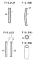
- FIGs.2(A) and 2(B) are horizontal and vertical cross sectional views showing a curved glass or plastic pane 1 to be fitted in the front window of a motor car, the pane 1 being coated with a carbonaceous film 45 of from 0.1 to 8mm thickness.
- the whole surface of the glass pane 1 may be coated with carbon film in accordance with the present invention, or alternatively only one side of the pane may be coated. In the latter case, panes treated in the apparatus shown in Fig. 1 may be disposed in parallel with each other in order to make pairs as illustrated in Fig.2(C).
- Figs. 3(A) and 3(B) illustrate a similar carbon coating formed on a cylindrical substrate.
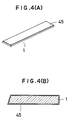
- Figs.4(A) and 4(B) illustrate a similar carbon coating formed on a plastic rule 1.
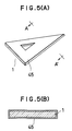
- Figs. 5(A) and 5(B) illustrate a 0.5mm carbon coating formed on a set square.
Landscapes
- Chemical & Material Sciences (AREA)
- Engineering & Computer Science (AREA)
- General Chemical & Material Sciences (AREA)
- Chemical Kinetics & Catalysis (AREA)
- Materials Engineering (AREA)
- Mechanical Engineering (AREA)
- Metallurgy (AREA)
- Organic Chemistry (AREA)
- Inorganic Chemistry (AREA)
- Physics & Mathematics (AREA)
- Plasma & Fusion (AREA)
- Chemical Vapour Deposition (AREA)
Description
- The present invention relates to an improved plasma processing method and apparatus. More particularly, but not exclusively, it relates to a method of adhering a protective film of carbonaceous material to comparatively soft substrates in order to provide a transparent electrically insulating coating thereon.
- Hard, thin films of diamond-like carbon have been deposited on substrates in a number of ways. By "diamond-like carbon" is meant carbon with exceptional hardness, e.g. which can neither be cut with a razor blade nor scratched by rubbing with steel wool. The chemical bonding of such diamond-like carbon appears to be dominated by sp³ tetrahedral diamond-like bonding as opposed to the sp² triagonal bonding of graphite. Diamond-like carbon films may or may not give evidence of crystallinity by x-rays.
- JP-A-56-146936 describes a process in which carbon deposition is carried out with the deposited carbon material being subjected to attack by accelerated ions at the same time so that soft portions of the deposited material are selectively removed to leave comparatively hard material. This technique is excellent for increasing the hardness of the carbon film thus deposited. Substrates to be coated in accordance with this technique, however, have to be given bias voltages in order to cause sputtering action thereon. For this reason, the advantage of this technique is diminished when the substrates are made of insulating materials.
- EP-A-0327406 (forming part of the state of the art only under Article 54(3)) discloses a process for carbon deposition in a plasma process under vacuum in which there are provided a vacuum chamber, a vacuum pump, a gas introduction system for introducing a reactive gas into the chamber, a pair of electrodes in the vacuum chamber and a high frequency source for applying an A/C voltage across the electrodes to convert the reactive gas into a plasma. The substrates to be coated are held in a substrate holder which is electrically connected to a lower frequency A/C source.
- It is therefore an object of the present invention to provide a plasma processing apparatus and method which enables the above problems of the prior art to be overcome.
- Another object of the present invention is to provide a plasma processing method and apparatus which enables diamond-like carbonaceous films to be deposited onto substrates formed of electrically insulating materials.
- The above and other objects of the present invention may be accomplished by use of a plasma processing method and apparatus wherein ion bombardment of a substrate by ions of the plasma is achieved by provision of supplementary electrodes within the plasma region and application to said supplementary electrodes of a voltage such as to cause plasma ions to impact the substrate.
- More particularly, the present invention provides a plasma processing apparatus comprising:
a vacuum chamber;
a vacuum pump connected to said vacuum chamber in order to evacuate said chamber;
a gas introduction system connected to said vacuum chamber in order to input a reactive gas into said chamber;
a pair of first electrodes provided in said vacuum chamber;
a first voltage source for applying a first alternating voltage at a high frequency between said first electrodes in order to convert the reactive gas in said vacuum chamber into a plasma; and
a substrate holder for supporting a substrate to be treated by said apparatus between said first electrodes; characterised by
a pair of second electrodes arranged in order that the substrate supported by said holder is located between said second electrodes; and
a second voltage source for applying a second alternating voltage between said second electrodes, the frequency of said second alternating voltage being so low as to enable said plasma to follow it. - Thus in accordance with an exemplary embodiment of the invention, a pair of auxiliary electrodes are provided in a vacuum chamber on opposite sides of a substrate to be treated, in addition to other electrodes that are provided for producing plasma gas in the vacuum chamber. As compared to the high frequency voltage that is used for forming the plasma, a relatively low frequency voltage is applied between the auxiliary electrodes in order to cause the bombardment of ions of plasma upon the substrate.
- The invention also extends to a method of treating a substrate by plasma processing in a vacuum chamber comprising:
disposing said substrate between a pair of first electrodes in said vacuum chamber;
inputting a reactive gas into said vacuum chamber at an appropriate pressure; and
inputting a first alternating voltage between said first electrodes at a high frequency in order to produce a plasma from said reactive gas and to perform plasma processing of said substrate;
characterised in that a second alternating voltage is applied between a pair of second electrodes located to sandwich said substrate, said second alternating voltage being at a frequency at which said plasma can follow said second voltage. - By virtue of such plasma treatment in accordance with the present invention, hard films can be deposited since the bombardment of the forming coating with plasma ions tends to selectively remove soft portions of the material that is deposited during the deposition process. When carbonaceous films are formed by use of a plasma comprising a carbon compound gas, the hardness and the resistivity of the films can be controlled by adding a fluorine compound gas. The fluorine contained in the carbon film that is deposited functions also to enhance the water repellent property of the film. Such carbon films are suitable for protective coatings on glass windows of vehicles, for example.
- Other substrates suitable for treatment in accordance with the teachings of the present invention are made of, for example, insulating materials having resistivities not lower than 10¹⁵ ohm centimeters, such as polyesters, alkyd resins, oil-free alkyd resins, unsaturated polyesters, acrylic resins and amino-resins. Particularly, suitable organic material used in manufacture of motorcars are acrylic lacquers, acrylic melanins and block acrylic urethanes.
- Further features of the invention are set forth in the appended claims and, together with the above features, can be better understood from consideration of the following detailed description of exemplary embodiments when read in conjunction with the acompanying drawings.
-
- Fig.1 is a schematic cross sectional diagram showing a plasma CVD apparatus in accordance with one embodiment of the present invention;
- Figs.2(A) and 2(B) are vertical and horizontal cross sectional views showing a window glass for motor cars which has been coated with a carbon protective film in accordance with the present invention;
- Fig.2(C) is a schematic cross sectional view showing a modification of the embodiment shown in Figs.2(A) and 2(B);
- Figs.3(A) and 3(B) are horizontal and perspective cross sectional views showing a cylinder coated with a carbon protective film in accordance with the present invention;
- Figs.4(A) and 4(B) are perspective and cross sectional views showing a rule coated with a carbon protective film in accordance with the present invention; and
- Figs.5(A) and 5(B) are perspective and cross sectional views showing a set square coated with a carbon protective film in accordance with the present invention.
- Referring now to Fig.1, a chemical vapor deposition apparatus is illustrated. The apparatus comprises a
vacuum chamber 9 defining a deposition space therein, anevacuation system 25 comprising arotary pump 23 and a turbo-molecular pump 22 which are connected to thechamber 7 through avalve 21, agas supply system 30 comprising four gas supply lines, each being provided with aflow meter 29 and avalve 28, connected to thereaction chamber 7, a pair of mesh electrodes 3-1 and 3-2 made of aluminum and located at upper and lower positions inside of the deposition space, apower supply 40 for supplying energy to the mesh electrodes 3-1 and 3-2, a plurality ofsubstrate holders 20 forholding substrates 1, theholders 20 being connected to thechamber 7 throughcapacitors 19, a plurality of Al mesh electrodes 50 (13-n, 13′-n) interposed between adjacent substrates and outside of the first and last substrates, and a bias voltage applying means 17 for applying an AC voltage between adjacent ones of theelectrodes 50. Thereaction chamber 7 is provided with agate valve 9 through which substrates to be coated may be disposed in the chamber. - The
energy supply 40 comprises a first power source 15-1 which supplies an AC voltage to the mesh electrode 3-1 through a matching device 16-1 comprising a LCR circuit, a second power source 15-2 which supplies an AC voltage to the mesh electrode 3-2 through a matching device 16-2 comprising a LCR circuit, and aphase adjuster 26 connected between the first and second power sources 15-1 and 15-2. Both the first and second power sources are grounded at terminals 5-1 and 5-2. Thebias applying device 17 is provided with first and second AC voltage sources 17-1 and 17-2, which supply AC voltages between adjacent electrodes 13-n and 13-n'. One terminal of each of the voltage sources 17-1 and 17-2 is grounded at 5-3. - In operation, after evacuating the
chamber 7, a carbon compound gas is introduced into thedeposition space 8 at a pressure of from 0.133 to 133 Pa (0.001 to 1 Torr). For example, the carbon compound gas may consist of C₂F₆ and C₂H₄ in the ratio of from 1:4 to 4:1, e.g. 1:1, and may be introduced so that the pressure in thereaction chamber 7 becomes 67 Pa (0.5 Torr). The transparency and resistivity of the carbon material that is deposited can be controlled by changing the amount of fluorine contained in the carbon material through adjustment of the introduction rate of C₂F₆ relative to C₂H₄. The temperature in the deposition space is no higher than 150°C. High frequency alternating voltages of from 1 MHz to 100 MHz, e.g. 13.56 MHz, are applied to the mesh electrodes 3-1 and 3-2 from the first and second power sources 15-1 and 15-2. The phase difference between these high frequency voltages is adjusted to be O° or 180° by means of thephase adjuster 26. By virtue of the injections of such high frequency energy into the plasma chamber, the carbon compound gas is converted into a plasma state and carbon deposition onto the substrates occurs. The deposition rate is from 10nm to 100nm/min (100 to 1000 A°/min). The thickness of the deposited carbon films may be from 0.1 to 8mm on flat surfaces and from 1 to 3mm on uneven surfaces. - At the same time, an AC voltage is applied between adjacent electrodes 13-n and 13'-n in order to induce an electric field normal to the major surfaces of each substrate. The frequency of the AC voltage between the electrodes 13-n and 13'-n is selected to be in the range of from 10 Hz to 100 KHz, e.g., 50 Hz. At such comparatively low frequencies, plasma ions can follow the electric field and bombard the substrate surfaces on which carbon deposition is being carried out. As a result, softer deposited materials are removed so that the hardness of the carbon material that remains is relatively high, e.g. 600 to 6000 kg/mm². The resistivity of the carbon is, for example, from 1 x 10⁶ to 5 x 10¹² ohm centimeter, typically from 1 x 10⁷ to 1 x 10¹¹ ohm centimeter. The optical energy band gap is no narrower than 1.0 eV, typically 1.5 to 5.5 eV. The carbon material may include hydrogen at 30 atom% or less and fluorine at 0.3 to 10 atom%.
- Carbonaceous films were coated on several substrates in accordance with the present invention. Figs.2(A) and 2(B) are horizontal and vertical cross sectional views showing a curved glass or
plastic pane 1 to be fitted in the front window of a motor car, thepane 1 being coated with acarbonaceous film 45 of from 0.1 to 8mm thickness. The whole surface of theglass pane 1 may be coated with carbon film in accordance with the present invention, or alternatively only one side of the pane may be coated. In the latter case, panes treated in the apparatus shown in Fig. 1 may be disposed in parallel with each other in order to make pairs as illustrated in Fig.2(C). Figs. 3(A) and 3(B) illustrate a similar carbon coating formed on a cylindrical substrate. Figs.4(A) and 4(B) illustrate a similar carbon coating formed on aplastic rule 1. Figs. 5(A) and 5(B) illustrate a 0.5mm carbon coating formed on a set square. - While several embodiments have been specifically described by way of example, it is to be appreciated that the present invention is not limited to the particular examples described and that modifications and variations can be made. For example, the present invention is useful when front, side or rear windows or side mirrors are coated with carbon protective films.
Claims (11)
- A plasma processing apparatus comprising:
a vacuum chamber (9);
a vacuum pump (25) connected to said vacuum chamber in order to evacuate said chamber;
a gas introduction system (30) connected to said vacuum chamber in order to input a reactive gas into said chamber;
a pair of first electrodes (3-1, 3-2) provided in said vacuum chamber;
a first voltage source (40) for applying a first alternating voltage at a high frequency between said first electrodes in order to convert the reactive gas in said vacuum chamber into a plasma; and
a substrate holder (20) for supporting a substrate to be treated by said apparatus between said first electrodes; characterised by
a pair of second electrodes (13-n, 13'-n) arranged in order that the substrate supported by said holder (20) is located between said second electrodes; and
a second voltage source (17) for applying a second alternating voltage between said second electrodes, the frequency of said second alternating voltage being so low as to enable said plasma to follow it. - The apparatus of claim 1 wherein the frequency of said first alternating voltage is selected to be in the range of 1 MHz to 50 MHz.
- The apparatus of claim 2 wherein the frequency of said second alternating voltage is selected to be in the range of 10 Hz to 100 KHz.
- The apparatus of any of claims 1 to 3 wherein said substrate holder (20) is adapted to support a plurality of substrates arranged in parallel with each other.
- The apparatus of claim 4 wherein said second electrodes (13-n, 13'-n) are located between adjacent ones of said substrates.
- A method of treating a substrate by plasma processing in a vacuum chamber (9) comprising:
disposing said substrate between a pair of first electrodes (3-1, 3-2) in said vacuum chamber (9);
inputting a reactive gas into said vacuum chamber (9) at an appropriate pressure; and
inputting a first alternating voltage between said first electrodes (3-1, 3-2) at a high frequency in order to produce a plasma from said reactive gas and to perform plasma processing of said substrate;
characterised in that a second alternating voltage is applied between a pair of second electrodes (13-n, 13'-n) located to sandwich said substrate, said second alternating voltage being at a frequency at which said plasma can follow said second voltage. - The method of claim 6 wherein said substrate is made from an insulating material.
- The method of claim 6 or 7 wherein said reactive gas is decomposed in order to deposit a film on said substrate.
- The method of claim 6 or 7 or 8 wherein said reactive gas is a carbon compound gas.
- The method of any of claims 6 to 9 wherein said film comprises diamond-like carbon.
- A plasma CVD method utilizing a vacuum chamber (9) having two sets of electrodes (3-1, 3-2, 13-n, 13'-n), and wherein a high frequency voltage is applied between one set of electrodes (3-1, 3-2) in order to produce a plasma from a reactive gas introduced into the chamber (9), a substrate to be coated is operatively located relative to and spaced from the other set of electrodes (13-n, 13'-n), and a relatively low frequency voltage is applied to the other set of electrodes (13-n, 13'-n) for effecting bombardment of the substrate surface with plasma ions whereby relatively soft parts of the coating being deposited will be removed leaving only harder material.
Applications Claiming Priority (6)
| Application Number | Priority Date | Filing Date | Title |
|---|---|---|---|
| JP233166/88 | 1988-09-16 | ||
| JP233168/88 | 1988-09-16 | ||
| JP23316788A JP2627939B2 (en) | 1988-09-16 | 1988-09-16 | Office materials covered with carbon film |
| JP23316688A JP2736421B2 (en) | 1988-09-16 | 1988-09-16 | Member covered with carbon film and method of manufacturing the same |
| JP233167/88 | 1988-09-16 | ||
| JP63233168A JP2639569B2 (en) | 1988-09-16 | 1988-09-16 | Plasma reaction method and plasma reaction apparatus |
Publications (3)
| Publication Number | Publication Date |
|---|---|
| EP0359567A2 EP0359567A2 (en) | 1990-03-21 |
| EP0359567A3 EP0359567A3 (en) | 1991-01-16 |
| EP0359567B1 true EP0359567B1 (en) | 1994-08-17 |
Family
ID=27331961
Family Applications (1)
| Application Number | Title | Priority Date | Filing Date |
|---|---|---|---|
| EP89309352A Expired - Lifetime EP0359567B1 (en) | 1988-09-16 | 1989-09-14 | Plasma processing method and apparatus |
Country Status (4)
| Country | Link |
|---|---|
| US (1) | US5041201A (en) |
| EP (1) | EP0359567B1 (en) |
| KR (1) | KR920007022B1 (en) |
| DE (1) | DE68917550T2 (en) |
Families Citing this family (21)
| Publication number | Priority date | Publication date | Assignee | Title |
|---|---|---|---|---|
| US5283087A (en) * | 1988-02-05 | 1994-02-01 | Semiconductor Energy Laboratory Co., Ltd. | Plasma processing method and apparatus |
| US5688556A (en) * | 1994-04-01 | 1997-11-18 | Mobil Oil Corporation | Barrier films having vapor coated EVOH surfaces |
| JPH09511193A (en) * | 1994-04-01 | 1997-11-11 | モービル・オイル・コーポレーション | Barrier film with carbon-coated high energy surface |
| ZA954295B (en) * | 1994-06-03 | 1996-11-25 | Mobil Oil Corp | Carbon-coated barrier films with increased concentration of tetrahedrally-coordinated carbon |
| JP2788412B2 (en) * | 1994-08-11 | 1998-08-20 | 麒麟麦酒株式会社 | Apparatus and method for producing carbon film-coated plastic container |
| US5656123A (en) * | 1995-06-07 | 1997-08-12 | Varian Associates, Inc. | Dual-frequency capacitively-coupled plasma reactor for materials processing |
| FR2738832B1 (en) * | 1995-09-18 | 1997-12-12 | Suisse Electronique Microtech | PROCESS FOR OBTAINING A DIAMOND LAYER ON A PLASTIC SUPPORT AND PRODUCT THUS OBTAINED |
| DE69624139T2 (en) * | 1995-12-01 | 2003-06-12 | E.I. Du Pont De Nemours And Co., Wilmington | CAPACITATIVE COUPLED RF REACTOR FOR COATING WITH DIAMOND-LIKE CARBON |
| JP3669138B2 (en) * | 1998-03-05 | 2005-07-06 | 日新電機株式会社 | Plasma CVD method, plasma CVD apparatus and electrode |
| US6528435B1 (en) * | 2000-08-25 | 2003-03-04 | Wafermasters, Inc. | Plasma processing |
| TW544071U (en) * | 2002-04-02 | 2003-07-21 | Nano Electronics And Micro Sys | Electrode device for plasma treatment system |
| JP2004288984A (en) * | 2003-03-24 | 2004-10-14 | Sharp Corp | Film forming apparatus and film forming method |
| DE10317208A1 (en) * | 2003-04-15 | 2004-11-04 | Robert Bosch Gmbh | Plasma deposition process |
| KR20060115734A (en) * | 2003-10-28 | 2006-11-09 | 노드슨 코포레이션 | Plasma Processing System and Plasma Processing Method |
| US7824498B2 (en) * | 2004-02-24 | 2010-11-02 | Applied Materials, Inc. | Coating for reducing contamination of substrates during processing |
| JP4185483B2 (en) * | 2004-10-22 | 2008-11-26 | シャープ株式会社 | Plasma processing equipment |
| JP4584722B2 (en) * | 2005-01-13 | 2010-11-24 | シャープ株式会社 | Plasma processing apparatus and semiconductor device manufactured by the same |
| JP2006196681A (en) * | 2005-01-13 | 2006-07-27 | Sharp Corp | Plasma processing apparatus and semiconductor device manufactured by the same |
| US8372238B2 (en) | 2008-05-20 | 2013-02-12 | Nordson Corporation | Multiple-electrode plasma processing systems with confined process chambers and interior-bussed electrical connections with the electrodes |
| US8226795B2 (en) | 2009-02-03 | 2012-07-24 | Nordson Corporation | Magnetic clips and substrate holders for use in a plasma processing system |
| CN113755818A (en) * | 2020-06-02 | 2021-12-07 | 阿里山钻石科技股份有限公司 | Diamond manufacturing apparatus, diamond manufacturing method using the same, and diamond inspection method |
Family Cites Families (10)
| Publication number | Priority date | Publication date | Assignee | Title |
|---|---|---|---|---|
| JPS6029295B2 (en) * | 1979-08-16 | 1985-07-10 | 舜平 山崎 | Non-single crystal film formation method |
| JPS5930709A (en) * | 1982-08-13 | 1984-02-18 | Toa Nenryo Kogyo Kk | Method for synthesizing carbon film and carbon granule in vapor phase |
| US4464223A (en) * | 1983-10-03 | 1984-08-07 | Tegal Corp. | Plasma reactor apparatus and method |
| JPH0644554B2 (en) * | 1984-03-28 | 1994-06-08 | 株式会社富士電機総合研究所 | Plasma CVD equipment |
| JP2616760B2 (en) * | 1985-04-08 | 1997-06-04 | 株式会社 半導体エネルギー研究所 | Plasma gas phase reactor |
| CN1020477C (en) * | 1987-08-10 | 1993-05-05 | 株式会社半导体能源研究所 | Halogen-containing carbon material deposition method |
| JPS6461396A (en) * | 1987-09-01 | 1989-03-08 | Idemitsu Petrochemical Co | Synthesis of diamond and installation therefor |
| KR920003431B1 (en) * | 1988-02-05 | 1992-05-01 | 가부시끼가이샤 한도다이 에네르기 겐뀨쇼 | Plasma processing method and apparatus |
| KR930010193B1 (en) * | 1988-09-13 | 1993-10-15 | 가부시끼가이샤 한도다이 에네르기겐뀨쇼 | Parts covered with ceramic film and carbon film and manufacturing method |
| US5185179A (en) * | 1988-10-11 | 1993-02-09 | Semiconductor Energy Laboratory Co., Ltd. | Plasma processing method and products thereof |
-
1989
- 1989-09-07 US US07/403,821 patent/US5041201A/en not_active Expired - Lifetime
- 1989-09-11 KR KR1019890013120A patent/KR920007022B1/en not_active Expired
- 1989-09-14 EP EP89309352A patent/EP0359567B1/en not_active Expired - Lifetime
- 1989-09-14 DE DE68917550T patent/DE68917550T2/en not_active Expired - Fee Related
Also Published As
| Publication number | Publication date |
|---|---|
| US5041201A (en) | 1991-08-20 |
| KR900005854A (en) | 1990-04-14 |
| EP0359567A2 (en) | 1990-03-21 |
| DE68917550T2 (en) | 1994-12-22 |
| DE68917550D1 (en) | 1994-09-22 |
| EP0359567A3 (en) | 1991-01-16 |
| KR920007022B1 (en) | 1992-08-24 |
Similar Documents
| Publication | Publication Date | Title |
|---|---|---|
| EP0359567A2 (en) | Plasma processing method and apparatus | |
| EP0372696B1 (en) | Method of producing a carbon-based film | |
| EP3711078B1 (en) | Linearized energetic radio-frequency plasma ion source | |
| US4869923A (en) | Microwave enhanced CVD method for depositing carbon | |
| US4971667A (en) | Plasma processing method and apparatus | |
| KR930003605B1 (en) | Microwave enhanced cvd method for coating plastic articles with carbon films and its products | |
| EP0474369B1 (en) | Diamond-like carbon coatings | |
| PL186562B1 (en) | Method of covering edges with diamond carbon | |
| US6001432A (en) | Apparatus for forming films on a substrate | |
| US4512284A (en) | Glow discharge apparatus for use in coating a disc-shaped substrate | |
| EP0846792B1 (en) | Method of synthesizing diamond | |
| US7144629B2 (en) | Electrostatic-erasing abrasion-proof coating and method for forming the same | |
| US5628920A (en) | Organic layer for subsequent coating with a cover layer which is harder than the organic layer and process for surface treatment of an organic layer | |
| JPH07258840A (en) | Carbon thin film forming method | |
| CN1025353C (en) | Plasma treatment method and apparatus | |
| US5270029A (en) | Carbon substance and its manufacturing method | |
| CA2061302C (en) | Method of making synthetic diamond film | |
| Okamoato et al. | Formation and properties of cubic boron nitride films on tungsten carbide by plasma chemical vapor deposition | |
| Westwood | Reactive sputtering: introduction and general discussion | |
| JP3083008B2 (en) | Film forming apparatus and film forming method | |
| US5127988A (en) | Process for the surface treatment of conductive material | |
| JPH0769790A (en) | Thin film production equipment | |
| EP0747501A1 (en) | Thin film deposition | |
| Dellafera et al. | An alternative method of preparing hydrogen-doped evaporated amorphous silicon preliminary report | |
| JPH09125243A (en) | Thin film forming equipment |
Legal Events
| Date | Code | Title | Description |
|---|---|---|---|
| PUAI | Public reference made under article 153(3) epc to a published international application that has entered the european phase |
Free format text: ORIGINAL CODE: 0009012 |
|
| AK | Designated contracting states |
Kind code of ref document: A2 Designated state(s): DE FR GB |
|
| PUAL | Search report despatched |
Free format text: ORIGINAL CODE: 0009013 |
|
| AK | Designated contracting states |
Kind code of ref document: A3 Designated state(s): DE FR GB |
|
| 17P | Request for examination filed |
Effective date: 19910308 |
|
| 17Q | First examination report despatched |
Effective date: 19920814 |
|
| GRAA | (expected) grant |
Free format text: ORIGINAL CODE: 0009210 |
|
| AK | Designated contracting states |
Kind code of ref document: B1 Designated state(s): DE FR GB |
|
| REF | Corresponds to: |
Ref document number: 68917550 Country of ref document: DE Date of ref document: 19940922 |
|
| ET | Fr: translation filed | ||
| PLBE | No opposition filed within time limit |
Free format text: ORIGINAL CODE: 0009261 |
|
| STAA | Information on the status of an ep patent application or granted ep patent |
Free format text: STATUS: NO OPPOSITION FILED WITHIN TIME LIMIT |
|
| 26N | No opposition filed | ||
| PGFP | Annual fee paid to national office [announced via postgrant information from national office to epo] |
Ref country code: GB Payment date: 19950905 Year of fee payment: 7 |
|
| PGFP | Annual fee paid to national office [announced via postgrant information from national office to epo] |
Ref country code: FR Payment date: 19950911 Year of fee payment: 7 |
|
| PGFP | Annual fee paid to national office [announced via postgrant information from national office to epo] |
Ref country code: DE Payment date: 19950918 Year of fee payment: 7 |
|
| PG25 | Lapsed in a contracting state [announced via postgrant information from national office to epo] |
Ref country code: GB Effective date: 19960914 |
|
| PG25 | Lapsed in a contracting state [announced via postgrant information from national office to epo] |
Ref country code: FR Effective date: 19960930 |
|
| GBPC | Gb: european patent ceased through non-payment of renewal fee |
Effective date: 19960914 |
|
| PG25 | Lapsed in a contracting state [announced via postgrant information from national office to epo] |
Ref country code: DE Effective date: 19970603 |
|
| REG | Reference to a national code |
Ref country code: FR Ref legal event code: ST |
|
| REG | Reference to a national code |
Ref country code: FR Ref legal event code: ST |