EP0354811B1 - Superconductive photoconductive substance of the Ba-Pb-Bi-O group system and a method for producing the same - Google Patents
Superconductive photoconductive substance of the Ba-Pb-Bi-O group system and a method for producing the same Download PDFInfo
- Publication number
- EP0354811B1 EP0354811B1 EP89308201A EP89308201A EP0354811B1 EP 0354811 B1 EP0354811 B1 EP 0354811B1 EP 89308201 A EP89308201 A EP 89308201A EP 89308201 A EP89308201 A EP 89308201A EP 0354811 B1 EP0354811 B1 EP 0354811B1
- Authority
- EP
- European Patent Office
- Prior art keywords
- photoconductivity
- substance
- photoconductive
- oxide
- temperature
- Prior art date
- Legal status (The legal status is an assumption and is not a legal conclusion. Google has not performed a legal analysis and makes no representation as to the accuracy of the status listed.)
- Expired - Lifetime
Links
- 239000000126 substance Substances 0.000 title claims description 38
- 238000004519 manufacturing process Methods 0.000 title claims description 5
- 239000000203 mixture Substances 0.000 claims description 36
- 238000000034 method Methods 0.000 claims description 21
- 238000005245 sintering Methods 0.000 claims description 14
- 230000000694 effects Effects 0.000 claims description 7
- 239000000463 material Substances 0.000 claims description 7
- 238000001816 cooling Methods 0.000 claims description 6
- 238000010438 heat treatment Methods 0.000 claims description 5
- 239000007858 starting material Substances 0.000 claims description 5
- 238000003746 solid phase reaction Methods 0.000 claims description 4
- 230000005684 electric field Effects 0.000 claims description 3
- 238000007493 shaping process Methods 0.000 claims description 3
- 230000001360 synchronised effect Effects 0.000 claims description 3
- 230000001443 photoexcitation Effects 0.000 claims 1
- WMWLMWRWZQELOS-UHFFFAOYSA-N bismuth(iii) oxide Chemical compound O=[Bi]O[Bi]=O WMWLMWRWZQELOS-UHFFFAOYSA-N 0.000 description 26
- 239000002887 superconductor Substances 0.000 description 18
- AYJRCSIUFZENHW-UHFFFAOYSA-L barium carbonate Chemical compound [Ba+2].[O-]C([O-])=O AYJRCSIUFZENHW-UHFFFAOYSA-L 0.000 description 12
- 230000003287 optical effect Effects 0.000 description 9
- 230000005284 excitation Effects 0.000 description 8
- 238000005259 measurement Methods 0.000 description 8
- 229910052760 oxygen Inorganic materials 0.000 description 7
- 239000004065 semiconductor Substances 0.000 description 6
- 239000012212 insulator Substances 0.000 description 5
- YEXPOXQUZXUXJW-UHFFFAOYSA-N lead(II) oxide Inorganic materials [Pb]=O YEXPOXQUZXUXJW-UHFFFAOYSA-N 0.000 description 5
- 238000002156 mixing Methods 0.000 description 5
- 230000005283 ground state Effects 0.000 description 4
- 230000005693 optoelectronics Effects 0.000 description 4
- 239000001301 oxygen Substances 0.000 description 4
- 239000012071 phase Substances 0.000 description 4
- 238000001228 spectrum Methods 0.000 description 4
- 230000003068 static effect Effects 0.000 description 4
- 230000001052 transient effect Effects 0.000 description 4
- 229910002480 Cu-O Inorganic materials 0.000 description 3
- QVGXLLKOCUKJST-UHFFFAOYSA-N atomic oxygen Chemical compound [O] QVGXLLKOCUKJST-UHFFFAOYSA-N 0.000 description 3
- 230000000903 blocking effect Effects 0.000 description 3
- 239000002772 conduction electron Substances 0.000 description 3
- 238000002474 experimental method Methods 0.000 description 3
- 230000004044 response Effects 0.000 description 3
- 238000010583 slow cooling Methods 0.000 description 3
- 230000003595 spectral effect Effects 0.000 description 3
- 229910009203 Y-Ba-Cu-O Inorganic materials 0.000 description 2
- 238000010521 absorption reaction Methods 0.000 description 2
- 230000015572 biosynthetic process Effects 0.000 description 2
- 230000002596 correlated effect Effects 0.000 description 2
- 230000008878 coupling Effects 0.000 description 2
- 238000010168 coupling process Methods 0.000 description 2
- 238000005859 coupling reaction Methods 0.000 description 2
- 239000013078 crystal Substances 0.000 description 2
- 238000010586 diagram Methods 0.000 description 2
- 230000003993 interaction Effects 0.000 description 2
- 150000002500 ions Chemical class 0.000 description 2
- 230000007246 mechanism Effects 0.000 description 2
- 230000000704 physical effect Effects 0.000 description 2
- 239000013558 reference substance Substances 0.000 description 2
- 230000001105 regulatory effect Effects 0.000 description 2
- 230000003252 repetitive effect Effects 0.000 description 2
- 239000000523 sample Substances 0.000 description 2
- 239000000654 additive Substances 0.000 description 1
- 229910045601 alloy Inorganic materials 0.000 description 1
- 239000000956 alloy Substances 0.000 description 1
- 238000000137 annealing Methods 0.000 description 1
- 238000013459 approach Methods 0.000 description 1
- 229910052788 barium Inorganic materials 0.000 description 1
- DSAJWYNOEDNPEQ-UHFFFAOYSA-N barium atom Chemical compound [Ba] DSAJWYNOEDNPEQ-UHFFFAOYSA-N 0.000 description 1
- 230000001427 coherent effect Effects 0.000 description 1
- 150000001875 compounds Chemical class 0.000 description 1
- 238000007796 conventional method Methods 0.000 description 1
- 230000000875 corresponding effect Effects 0.000 description 1
- 238000011156 evaluation Methods 0.000 description 1
- 239000004615 ingredient Substances 0.000 description 1
- HTUMBQDCCIXGCV-UHFFFAOYSA-N lead oxide Chemical compound [O-2].[Pb+2] HTUMBQDCCIXGCV-UHFFFAOYSA-N 0.000 description 1
- 230000031700 light absorption Effects 0.000 description 1
- 230000005415 magnetization Effects 0.000 description 1
- 229910052751 metal Inorganic materials 0.000 description 1
- 239000002184 metal Substances 0.000 description 1
- 150000002739 metals Chemical class 0.000 description 1
- 238000010606 normalization Methods 0.000 description 1
- 239000013307 optical fiber Substances 0.000 description 1
- 238000010587 phase diagram Methods 0.000 description 1
- 239000000843 powder Substances 0.000 description 1
- 230000035945 sensitivity Effects 0.000 description 1
- 229910052712 strontium Inorganic materials 0.000 description 1
- CIOAGBVUUVVLOB-UHFFFAOYSA-N strontium atom Chemical compound [Sr] CIOAGBVUUVVLOB-UHFFFAOYSA-N 0.000 description 1
- 238000006467 substitution reaction Methods 0.000 description 1
- 230000009897 systematic effect Effects 0.000 description 1
- 230000007704 transition Effects 0.000 description 1
Images




Classifications
-
- H—ELECTRICITY
- H10—SEMICONDUCTOR DEVICES; ELECTRIC SOLID-STATE DEVICES NOT OTHERWISE PROVIDED FOR
- H10N—ELECTRIC SOLID-STATE DEVICES NOT OTHERWISE PROVIDED FOR
- H10N60/00—Superconducting devices
- H10N60/80—Constructional details
- H10N60/85—Superconducting active materials
- H10N60/855—Ceramic superconductors
-
- C—CHEMISTRY; METALLURGY
- C04—CEMENTS; CONCRETE; ARTIFICIAL STONE; CERAMICS; REFRACTORIES
- C04B—LIME, MAGNESIA; SLAG; CEMENTS; COMPOSITIONS THEREOF, e.g. MORTARS, CONCRETE OR LIKE BUILDING MATERIALS; ARTIFICIAL STONE; CERAMICS; REFRACTORIES; TREATMENT OF NATURAL STONE
- C04B35/00—Shaped ceramic products characterised by their composition; Ceramics compositions; Processing powders of inorganic compounds preparatory to the manufacturing of ceramic products
- C04B35/01—Shaped ceramic products characterised by their composition; Ceramics compositions; Processing powders of inorganic compounds preparatory to the manufacturing of ceramic products based on oxide ceramics
- C04B35/45—Shaped ceramic products characterised by their composition; Ceramics compositions; Processing powders of inorganic compounds preparatory to the manufacturing of ceramic products based on oxide ceramics based on copper oxide or solid solutions thereof with other oxides
- C04B35/4521—Shaped ceramic products characterised by their composition; Ceramics compositions; Processing powders of inorganic compounds preparatory to the manufacturing of ceramic products based on oxide ceramics based on copper oxide or solid solutions thereof with other oxides containing bismuth oxide
- C04B35/4525—Shaped ceramic products characterised by their composition; Ceramics compositions; Processing powders of inorganic compounds preparatory to the manufacturing of ceramic products based on oxide ceramics based on copper oxide or solid solutions thereof with other oxides containing bismuth oxide also containing lead oxide
-
- C—CHEMISTRY; METALLURGY
- C04—CEMENTS; CONCRETE; ARTIFICIAL STONE; CERAMICS; REFRACTORIES
- C04B—LIME, MAGNESIA; SLAG; CEMENTS; COMPOSITIONS THEREOF, e.g. MORTARS, CONCRETE OR LIKE BUILDING MATERIALS; ARTIFICIAL STONE; CERAMICS; REFRACTORIES; TREATMENT OF NATURAL STONE
- C04B35/00—Shaped ceramic products characterised by their composition; Ceramics compositions; Processing powders of inorganic compounds preparatory to the manufacturing of ceramic products
- C04B35/622—Forming processes; Processing powders of inorganic compounds preparatory to the manufacturing of ceramic products
- C04B35/64—Burning or sintering processes
-
- H—ELECTRICITY
- H10—SEMICONDUCTOR DEVICES; ELECTRIC SOLID-STATE DEVICES NOT OTHERWISE PROVIDED FOR
- H10F—INORGANIC SEMICONDUCTOR DEVICES SENSITIVE TO INFRARED RADIATION, LIGHT, ELECTROMAGNETIC RADIATION OF SHORTER WAVELENGTH OR CORPUSCULAR RADIATION
- H10F77/00—Constructional details of devices covered by this subclass
- H10F77/10—Semiconductor bodies
- H10F77/12—Active materials
-
- Y—GENERAL TAGGING OF NEW TECHNOLOGICAL DEVELOPMENTS; GENERAL TAGGING OF CROSS-SECTIONAL TECHNOLOGIES SPANNING OVER SEVERAL SECTIONS OF THE IPC; TECHNICAL SUBJECTS COVERED BY FORMER USPC CROSS-REFERENCE ART COLLECTIONS [XRACs] AND DIGESTS
- Y10—TECHNICAL SUBJECTS COVERED BY FORMER USPC
- Y10S—TECHNICAL SUBJECTS COVERED BY FORMER USPC CROSS-REFERENCE ART COLLECTIONS [XRACs] AND DIGESTS
- Y10S505/00—Superconductor technology: apparatus, material, process
- Y10S505/775—High tc, above 30 k, superconducting material
- Y10S505/784—Bismuth-, e.g. BaKBiO
Definitions
- This invention relates to superconductive photoconductive oxide.
- the inventor performed experiments on optical properties, especially on the photoconductivity in response to high-speed pulses, of those oxides whose composition is outside that of regular oxide superconductors, and the inventor has found that oxides with a chemical formula Ba-Pb 1-x -Bi x -O z , x being 0.35 to 1 and z being 2.7 to 3, revealed an unexpected correlation between the superconductivity and the photoconductivity thereof.
- the invention also relates to a method for production of the above oxide.
- the oxide has an x value of not smaller than 0.35 (x ⁇ 0.35) or is quickly cooled, it becomes a semiconductor having photoconductivity.
- the oxide has an x value of about 0.35 (x ⁇ 0.35) or is slowly cooled, it becomes a superconductor correlated with photoconductivity.
- the oxide of the invention is expected to be very useful in the industrial field of superconductive optoelectronics.
- an object of the present invention is to provide superconductive photoconductive substance which reveals superconductive photoconductivity or both superconductivity and photoconductivity at a temperature below its critical temperature for superconductivity or even above.
- the superconductive photoconductive substance according to the invention has a general chemical formula of Ba-Pb 1-x -Bi x -O z , x being 0.35 to 1 and z being 2.7 to 3 (but excluding compositions with x ⁇ 0.35 when z being 2.81 to 3), and the substance has a potential superconductivity at a temperature below 14 K and simultaneously has a photoconductivity at a temperature below 160 K depending on the value of the above x, the photoconductivity being valid at least in an exciting wavelength range of 500 to 700 nm.
- Another object of the present invention is to provide a method for producing the above-mentioned superconductive photoconductive substance which has photoconductivity correlated with superconductivity and has both superconductivity and photoconductivity.
- a mixture of starting materials is prepared for oxide with a general chemical formula of Ba-Pb 1-x -Bi x -O z , x being 0.35 to 1 and z being 2.7 ton 3 (but excluding compositions with x ⁇ 0.35 when z being 2.81 to 3), and the mixture is heated at 750-850°C for 2-10 hours so as to cause solid phase reaction in the mixture.
- the heated materials are gradually cooled, and they are shaped under pressure and heated again at 500-850°C for 2-10 hours so as to effect secondary sintering thereon.
- the secondarily sintered materials are kept at 600-500°C for 2-3 hours, and then cooled either extremely quickly at a rate of 1500-900°C/sec or slowly at a rate of 150-200°C/hour, whereby the desired superconductive photoconducting oxide is produced.
- the reason for limiting the composition of the oxide of the invention to the above-mentioned general chemical formula is in that the oxide of such composition reveals photoconductivity associated with superconductivity, or reveals both superconductivity and photoconductivity provided that it is treated by the method of the invention; namely, the method comprising steps of heating at about 750-850°C for 2-10 hours so as to cause solid phase reaction among starting materials thereof, cooling gradually, shaping under pressure, secondarily sintering at 500-850°C for 2-10 hours, keeping at 600-500°C for 2-3 hours, and then cooling either extremely quickly at a rate of 1500-900°C/sec or slowly at a rate of 150-200°C/hour.
- Fig. 1 shows a curve of superconductivity critical temperature Tsc and a curve of photoconductivity critical temperature Tpc for a wavelength range of 500-700 nm, both curves being for the Ba-Pb-Bi-O system oxide including the composition of the invention Ba-Pb 1-x -Bi x -O z . Below the superconductivity critical temperature Tsc the oxide can become superconductive, and below the critical temperature Tpc the oxide can become photoconductive in response to incident light of the above wavelength range.
- M stands for a metallic domain
- S stands for a semiconductor domain.
- the inventor has shown that, even in the insulator domain, the temperature-dependence and exciting-wavelength-dependence of the photoconductivity implicate the presence of potential superconductivity, as will be made clear by ensuing Embodiments (refer to Fig. 1). Whereby, the invention has been accomplished.
- composition of the oxide found by the inventor can be expressed by a chemical formula of Ba-Pb 1-x -Bi x -O3.
- the inventor has tried to seek into details of the complete scheme, especially optical properties in visible wavelength range, of the phase diagram of such oxide.
- the inventor's studies covered not only the superconductive phase of the above oxide but also semiconductive phase and insulating phase thereof.
- a large number of specimens of Ba-Bi-O and Ba-Pb-Bi-O systems were made from the powders of BaCO3, PbO and Bi2O3 by using the method already described in numerous references. For instance, primary sintering of a mixture of starting materials was effected at 750-900°C so as to cause solid phase reaction for primary sintering of the mixture. After being cooled gradually, the sintered mixture was shaped under pressure, and secondary sintering was effected at 800-850°C. The specimens were then annealed at 500-600°C and then cooled slowly.
- composition of the starting materials was studied in detail, and the composition of the specimen was selected to be close to regular superconductors in such a manner that it became more or less controllable in a range outside that of the latter. Besides, the value of z in the above chemical formula was controlled by carefully regulating the method and speed of cooling.
- Specimen #S54 with a composition of Ba-Bi-O3 was prepared by primary sintering of a starting mixture of that composition at 800-850°C for 2 hours, slow cooling, shaping under pressure, secondary sintering at 800°C for 2 hours, annealing at 600°C for 2 hours, and slow cooling.
- a specimen #B03 was prepared by using Bi2O3 through the same heat treatment as above.
- the specimen #S54 was made by mixing 0.986 g of BaCO3 and 1.165 g of Bi2O3, and sintering the mixture so as to produce BaBiO3.
- the specimen #S129 was made by mixing 0.789 g of BaCO3, 0.745 g of Bi2O3, and 0.178 g of PbO, and sintering the mixture so as to produce BaPb 0.2 Bi 0.8 O3.
- the specimen #S128 was made by mixing 0.789 g of BaCO3, 0.559 g of Bi2O3, and 0.357 g of PbO, and sintering the mixture so as to produce BaPb 0.4 Bi 0.6 O3, while the specimen #S135 was made by mixing 0.789 g of BaCO3, 0.466 g of Bi2O3, and 0.446 g of PbO, and sintering the mixture so as to produce BaPb 0.5 Bi 0.5 O3. Further, the specimen #S60 was made by mixing 0.986 g of BaCO3, 0.465 g of Bi2O3, and 0.669 g of PbO, and sintering the mixture so as to produce BaPb 0.6 Bi 0.4 O3.
- z represents the amount of oxygen in the substance, and it varies depending on the sintering conditions so as to produce a variety of final products. In the subject studies, oxides with z in the proximity of 3 (z ⁇ 3) were checked in the main.
- Spectral responses were studied by selecting the wavelength ⁇ from a dye laser with a resolution ⁇ 1 nm while using an appropriate normalization procedure for incident power from the laser and spectral sensitivity of the pyroelectric detector. A possibility of heating of the specimens by light excitation was minimized and estimated to be negligible. Photocarrier density was of the order of or less than 105 to 107/cm3. All photosignals were normally detected in the synchronized mode by using the Boxcar integrator.
- Fig. 4A illustrates a typical spectrum of pulse-excited transient photoresponse Q( ⁇ , T) of the reference specimen #B03 Bi2O3 over wavelengths ⁇ of about 500-700 nm
- Fig. 4B illustrates a similar spectrum of the specimen #S54 Ba1-Bi1-O z (z being about 3)
- the "photoconductivity" of the specimen #S54 begins to appear at about 160 K, assumes a maximum value at 100-110 K, remains comparatively flat at 65-80 K and 30-40 K, decrease gradually with the temperature until 20 K, and increases again at the temperature below 20 K.
- both the insulator specimen #S54 and the semiconductor specimen #S60 which is close to a superconductor, increase their photoresponse Q( ⁇ , T).
- the specimen #S54 Ba-Bi-O3 is clearly an insulator and the specimen #S60 Ba1-Pb 1-x -Bi x -O z (x ⁇ 0.4, z ⁇ 3) is a semiconductor.
- their photoconductivity observed with the blocking electrodes is compatible with their superconductivity. This is probably due to the insulating part of specimen #S60.
- the specimen Ba-Bi-O3 such as specimen #S54 usually have brown color mixed with golden color.
- the specimen #S129 looks brown.
- Specimens like #S60 look regular reddish black.
- a polaron can be created either by the optical excitation here or substitution of Bi by Pb especially in the Ba-Bi-O system.
- Similar phenomena have been observed also in the Y-Cu-O, Y Ba-Cu-O and La-Cu-O systems. Consequently, the inventor believes that these studies of elementary excitations here must reveal the nature of the superconducting ground state. To the best knowledge of the inventor, this is the first clear experimental indications of the polarons and exciton mechanisms displayed in the high-T c superconductivity and the perfect diamagnetism as far as the oxides of the invention are concerned.
- a method for producing the above oxide has been also developed.
- the invention is an outcome of the inventor's theoretical and experimental studies on the "dynamical mechanism of polarons and excitons" for "high-temperature superconductivity" in a temperature range of 4.2 to 300 K.
- the inventor used the D.C. four-probe method and the repetitive pulse photoconductivity method for measurement of the conductivity, and the microwave SQUID for the measurement of static magnetic susceptibility.
- the proposed oxide of the invention will open a new scientific and industrial field, to be named as "superconductive optoelectronics", wherein superconductivity is directly controlled by light.
Landscapes
- Engineering & Computer Science (AREA)
- Chemical & Material Sciences (AREA)
- Ceramic Engineering (AREA)
- Manufacturing & Machinery (AREA)
- Structural Engineering (AREA)
- Materials Engineering (AREA)
- Organic Chemistry (AREA)
- Inorganic Chemistry (AREA)
- Inorganic Compounds Of Heavy Metals (AREA)
- Superconductor Devices And Manufacturing Methods Thereof (AREA)
- Superconductors And Manufacturing Methods Therefor (AREA)
- Optical Fibers, Optical Fiber Cores, And Optical Fiber Bundles (AREA)
- Conductive Materials (AREA)
- Compositions Of Oxide Ceramics (AREA)
Description
- This invention relates to superconductive photoconductive oxide. The inventor performed experiments on optical properties, especially on the photoconductivity in response to high-speed pulses, of those oxides whose composition is outside that of regular oxide superconductors, and the inventor has found that oxides with a chemical formula Ba-Pb1-x-Bix-Oz, x being 0.35 to 1 and z being 2.7 to 3, revealed an unexpected correlation between the superconductivity and the photoconductivity thereof.
- The invention also relates to a method for production of the above oxide. In the method, the ratio of the above element contents x and z is independently controlled for instance by changing x from 1 to 0.25, or by regulating the value of z through either quick cooling or slow cooling while keep x constant, e.g., at x=0.30. When the oxide has an x value of not smaller than 0.35 (x≧0.35) or is quickly cooled, it becomes a semiconductor having photoconductivity. On the other hand, when the oxide has an x value of about 0.35 (x≃0.35) or is slowly cooled, it becomes a superconductor correlated with photoconductivity. The oxide of the invention is expected to be very useful in the industrial field of superconductive optoelectronics.
- There has been no publications at all on such superconductor which has inherent photoconductivity, except the inventor's disclosure of Y3-x-Bax-Cuy-Oz group and La₂-Cu₁-Oz group substance in their academic papers and copending patent applications.
- Conventional superconductors are metals or alloys thereof in the main. Recently, much attention has been paid to high-temperature oxide superconductors, such as superconductors of Y-Ba-Cu-O group, and considerable amounts of additives such as barium (Ba) and strontium (Sr) are used to modify or eventually raise the superconductive critical temperature (Tc). Studies and measurements on the optical properties of the superconductive substances at and in the proximity of visible wavelengths have been limited to the study of reflection and scattering of light therefrom due to the metallic properties of such substance.
- It has been believed that light is simply reflected from the surface of a superconductor and is not allowed to enter therein. Study of optical properties, except the phenomena of reflection and scattering, has been treated as a completely different field from that of superconductivity in academic institutions, domestic and abroad, and in international conferences.
- The reason for it is in that, generally speaking, researchers have considered that superconductivity is incompatible with such physical properties as light absorption and photoconductivity and they have assumed that light irradiation in a wave number with the excess energy over the energy gap of the BCS theory will merely destroy the stability of superconductivity.
- However, there is the certain clear correlation between them, as proven in the case of Y-Ba-Cu-O group substance and the like. If any substance having such photoconductivity which is related to superconductivity or any substance having both superconductive capability and photoconductive capability is produced, a number of new electronic and optoelectronic devices may be developed; for instance, a superconductive phototransistor, a "superconductive optical computer" as a combination of the "superconductive computer" based on the Josephson devices and the "optical computer" proposed in optoelectronics both currently studied, "superconductive optical fiber", and the like.
- Therefore, an object of the present invention is to provide superconductive photoconductive substance which reveals superconductive photoconductivity or both superconductivity and photoconductivity at a temperature below its critical temperature for superconductivity or even above.
- The superconductive photoconductive substance according to the invention has a general chemical formula of Ba-Pb1-x-Bix-Oz, x being 0.35 to 1 and z being 2.7 to 3 (but excluding compositions with x≦0.35 when z being 2.81 to 3), and the substance has a potential superconductivity at a temperature below 14 K and simultaneously has a photoconductivity at a temperature below 160 K depending on the value of the above x, the photoconductivity being valid at least in an exciting wavelength range of 500 to 700 nm.
- Another object of the present invention is to provide a method for producing the above-mentioned superconductive photoconductive substance which has photoconductivity correlated with superconductivity and has both superconductivity and photoconductivity.
- With the method according to the invention, a mixture of starting materials is prepared for oxide with a general chemical formula of Ba-Pb1-x-Bix-Oz, x being 0.35 to 1 and z being 2.7 ton 3 (but excluding compositions with x≦0.35 when z being 2.81 to 3), and the mixture is heated at 750-850°C for 2-10 hours so as to cause solid phase reaction in the mixture. The heated materials are gradually cooled, and they are shaped under pressure and heated again at 500-850°C for 2-10 hours so as to effect secondary sintering thereon. The secondarily sintered materials are kept at 600-500°C for 2-3 hours, and then cooled either extremely quickly at a rate of 1500-900°C/sec or slowly at a rate of 150-200°C/hour, whereby the desired superconductive photoconducting oxide is produced.
- The reason for limiting the composition of the oxide of the invention to the above-mentioned general chemical formula is in that the oxide of such composition reveals photoconductivity associated with superconductivity, or reveals both superconductivity and photoconductivity provided that it is treated by the method of the invention; namely, the method comprising steps of heating at about 750-850°C for 2-10 hours so as to cause solid phase reaction among starting materials thereof, cooling gradually, shaping under pressure, secondarily sintering at 500-850°C for 2-10 hours, keeping at 600-500°C for 2-3 hours, and then cooling either extremely quickly at a rate of 1500-900°C/sec or slowly at a rate of 150-200°C/hour.
- The inventor has found that, as to the values of x and z of the general chemical formula of Ba-Pb1-x-Bix-Oz of the oxide of the invention, if x is unity (x=1) or close to unity, the oxide becomes insulating and shows semiconductive properties as well as photoconductive properties for certain wavelengths of light even with higher on set temperatures. On the other hand, as x departs from unity and approaches to about 0.35, the superconductive properties of the substance becomes more apparent while the photoconductive properties of the oxide is maintained with various on set temperatures. It is noted, however, that if x≦0.35 when z is in a range of 2.81 to 3, the oxide shows only superconductive properties and the photoconductive properties is lost, so that such oxide composition is excluded from the scope of the invention.
- For a better understanding of the invention, reference is made to the accompanying drawings, in which:
- Fig. 1 is a graph showing the relationship between the physical properties of the oxide of the invention at different temperatures and the Bi content thereof;
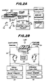
- Figs. 2A and 2B are diagrammatic illustrations of the principles of photoconductivity measurement by using blocking electrodes and applying repetitive electric and laser light pulses;
- Fig. 2C shows the time sequence and waveforms of pulses in the photoconductivity measurement;
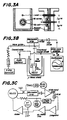
- Fig. 3A show sectional views of an essential part of a static susceptibility measuring device using a microwave SQUID (Superconducting Quantum Interference Device);
- Fig. 3B is a block diagram of the measuring system with the device of Fig. 3A;
- Fig. 3C is a block diagram of the feedback system with the device of Fig. 3A;
- Fig. 4A is a graph showing the wavelength-dependence of photoresponse Q(λ, T) of reference substance Bi₂O₃;
- Fig. 4B is a graph showing the wavelength-dependence of photoresponse Q(λ, T) of a superconductive photoconductive oxide of composition Ba₁BixO₃ (for x=1, i.e., Ba₁Bi₁O₃);
- Fig. 4C is a graph showing the wavelength-dependence of photoresponse Q(λ, T) of a superconductive photoconductive oxide of composition Ba₁Pb1-xBixO₃ (for x=0.5);
- Fig. 5A is a graph showing the temperature-dependence of photoresponse Q(λ, T) of the reference substance Bi₂O₃ for wavelength λ=660 nm;
- Fig. 5B is a graph showing the temperature-dependence of photoresponse Q(λ, T) of a superconductive photoconductive oxide of composition Ba₁Bi₁O₃ (x=1) for wavelength λ=520 nm; and
- Fig. 5C is a graph showing the temperature-dependence of photoresponse Q(λ, T) of a superconductive photoconductive oxide of composition Ba₁Pb1-xBixOz (x=0.5, 0.4 and z=3) for wavelength λ=528 nm.
- Fig. 1 shows a curve of superconductivity critical temperature Tsc and a curve of photoconductivity critical temperature Tpc for a wavelength range of 500-700 nm, both curves being for the Ba-Pb-Bi-O system oxide including the composition of the invention Ba-Pb1-x-Bix-Oz. Below the superconductivity critical temperature Tsc the oxide can become superconductive, and below the critical temperature Tpc the oxide can become photoconductive in response to incident light of the above wavelength range. In the figure, M stands for a metallic domain and S stands for a semiconductor domain.
- Of the oxide composition Ba-Pb1-x-Bix-Oz of the invention, ingredient element concentrations for making insulator are for instance x=0.40-1.0 and z=2.7-3, while those for making superconductor are for instance x=0.15-0.35 and z=2.81-3. The inventor has shown that, even in the insulator domain, the temperature-dependence and exciting-wavelength-dependence of the photoconductivity implicate the presence of potential superconductivity, as will be made clear by ensuing Embodiments (refer to Fig. 1). Whereby, the invention has been accomplished.
- Most of conventional oxide compounds such as Ba-Bi-Oz (z=2.7-3) and Ba-Pb1-x-Bix-Oz are normally semiconductors at the ground state, e.g., at low temperatures and in the dark. An elementary excitation can be created by giving a photon with a momentum of suitable magnitude and the corresponding amount of energy. Usually, for superconductors, these excitations beyond the energy gap destroy the superconductive ground state in the BCS theory. There is a possibility, however, to create a coherent state of elementary excitations above the ground state of insulating semiconductor such as bipolarons and excitons even in a thermally non-equilibrium state. We have found a new substance as an outcome of studies in fundamental physics and applied physics from the standpoint of the elementary excitation concept, in a sense parallel to, but rather orthogonal to the trend of studies of high-Tc (critical temperature) superconductors. Namely, our finding relates to substance whose composition does not result in perfect superconductor, but the substance has a composition close to that of superconductor and reveals superconductive photoconductivity both superconductivity and photoconductivity. The present invention has been completed based on that finding.
- The invention will be described in further detail by referring to embodiments.
- The composition of the oxide found by the inventor can be expressed by a chemical formula of Ba-Pb1-x-Bix-O₃. The inventor has tried to seek into details of the complete scheme, especially optical properties in visible wavelength range, of the phase diagram of such oxide. In particular, the inventor's studies covered not only the superconductive phase of the above oxide but also semiconductive phase and insulating phase thereof.
- A large number of specimens of Ba-Bi-O and Ba-Pb-Bi-O systems were made from the powders of BaCO₃, PbO and Bi₂O₃ by using the method already described in numerous references. For instance, primary sintering of a mixture of starting materials was effected at 750-900°C so as to cause solid phase reaction for primary sintering of the mixture. After being cooled gradually, the sintered mixture was shaped under pressure, and secondary sintering was effected at 800-850°C. The specimens were then annealed at 500-600°C and then cooled slowly. The composition of the starting materials was studied in detail, and the composition of the specimen was selected to be close to regular superconductors in such a manner that it became more or less controllable in a range outside that of the latter. Besides, the value of z in the above chemical formula was controlled by carefully regulating the method and speed of cooling.
- Specimens #S54 (z=1), #S129 (x=0.8), #S128 (x=0.6), #S135 (x=0.5) and #S60 (x=0.4) were prepared in the above-mentioned manner.
- Specimen #S54 with a composition of Ba-Bi-O₃ was prepared by primary sintering of a starting mixture of that composition at 800-850°C for 2 hours, slow cooling, shaping under pressure, secondary sintering at 800°C for 2 hours, annealing at 600°C for 2 hours, and slow cooling.
- As a reference specimen of Bi system, a specimen #B03 was prepared by using Bi₂O₃ through the same heat treatment as above.
- Since specimens of the a-Bi-Oz and Ba-Pb1-x-Bix-Oz systems within a certain value range of x and z became highly insulating for most values of x and z, or at least semiconducting at low temperatures, the conventional techniques for resistivity measurements encountered several serious difficulties. In particular, problems caused by combination of the non-ohmic contact electrodes, the buildup of space charge and with the low signal-to-noise ratio due to low carrier density in high-impedance materials were very difficult to overcome.
- In the experiments of the inventor, two types of techniques were adopted for resistivity and/or conductivity measurements. First, to measure the insulating specimen #S54 (ρ≧10⁸ Ω-cm), a fast pulse technique with blocking electrodes as shown in Figs. 2A and 2B was adopted. Referring to Fig. 2C, the difficulties noted above were overcome by using dye laser beam pulses of 3 ns width at a repetition rate of 13 Hz in the dark synchronized with pulse electric fields up to E≃5 kV/cm of 10 ms duration, so as to measure the photoresponse. Second, for moderately conducting specimens #S60 and #S135 (ρ≦10⁻²-10⁻¹ Ω-cm) at 300 K, regular resistive measurements were carried out by adopting the usual four-probe method without using light.
- The specimen #S54 was made by mixing 0.986 g of BaCO₃ and 1.165 g of Bi₂O₃, and sintering the mixture so as to produce BaBiO₃. The specimen #S129 was made by mixing 0.789 g of BaCO₃, 0.745 g of Bi₂O₃, and 0.178 g of PbO, and sintering the mixture so as to produce BaPb0.2Bi0.8O₃. Similarly, the specimen #S128 was made by mixing 0.789 g of BaCO₃, 0.559 g of Bi₂O₃, and 0.357 g of PbO, and sintering the mixture so as to produce BaPb0.4Bi0.6O₃, while the specimen #S135 was made by mixing 0.789 g of BaCO₃, 0.466 g of Bi₂O₃, and 0.446 g of PbO, and sintering the mixture so as to produce BaPb0.5Bi0.5O₃. Further, the specimen #S60 was made by mixing 0.986 g of BaCO₃, 0.465 g of Bi₂O₃, and 0.669 g of PbO, and sintering the mixture so as to produce BaPb0.6Bi0.4O₃. Here, z represents the amount of oxygen in the substance, and it varies depending on the sintering conditions so as to produce a variety of final products. In the subject studies, oxides with z in the proximity of 3 (z≃3) were checked in the main.
- Static magnetic susceptibility or magnetization itself was measured in weak fields up to H≃500 Oe by using a microwave SQUID (Superconducting Quantum Interference Device) at 9 GHz as shown in Figs. 3A, 3B and 3C. The knowledge on the superconductivity of the oxide of the above system belongs to the public, and what is important here is the properties of oxides with x≧0.35. Only the properties of the oxides with such value of x will be dealt with here without getting into details of the public knowledge.
- Spectral responses were studied by selecting the wavelength λ from a dye laser with a resolution Δλ≃1 nm while using an appropriate normalization procedure for incident power from the laser and spectral sensitivity of the pyroelectric detector. A possibility of heating of the specimens by light excitation was minimized and estimated to be negligible. Photocarrier density was of the order of or less than 10⁵ to 10⁷/cm³. All photosignals were normally detected in the synchronized mode by using the Boxcar integrator.
- The inventor observed definite signals of photoconductivity in all the specimens of Ba-Pb1-x-Bix-Oz, i.e., the specimens #S54 (x=1) through #S60 (x=0.40), by using the transient pulse technique described above.
- Firstly, the dependence of photoconductivity Q(λ,T,E,H) on the electric field E at 4.2 K was found to be substantially liner up to E≦4 kV/cm.
- Fig. 4A illustrates a typical spectrum of pulse-excited transient photoresponse Q(λ, T) of the reference specimen #B03 Bi₂O₃ over wavelengths λ of about 500-700 nm, Fig. 4B illustrates a similar spectrum of the specimen #S54 Ba₁-Bi₁-Oz (z being about 3), and Fig. 4C illustrates a similar spectrum of specimen #S135 Ba₁-Pb1-x-Bix-Oz (x=0.5, z≃3).
- Secondly, temperature dependence of the pulse-excited transient photoresponse Q(λ, T) in the wavelength range of λ≃500-700 nm was studied by using the reference specimen #B03, the insulator specimen #S54 and the specimen #S60 with a potential superconductivity. The results for the three specimens are shown in Fig. 5A, Fig. 5B, and Fig. 5C, respectively. Surprising, there definitely exists a systematic similarity of the transient photoresponse Q(λ, T) between the specimens #S54 and #S60, in spite of a huge difference in dark resistivity ρ(T) therebetween. The dark resistivity ρ(T) of the specimen #S54 is actually very large. As can be seen from Fig. 5B, with the decrease of temperature, the "photoconductivity" of the specimen #S54 begins to appear at about 160 K, assumes a maximum value at 100-110 K, remains comparatively flat at 65-80 K and 30-40 K, decrease gradually with the temperature until 20 K, and increases again at the temperature below 20 K. Thus, at the temperature below 20 K, both the insulator specimen #S54 and the semiconductor specimen #S60, which is close to a superconductor, increase their photoresponse Q(λ, T).
- Finally, the dark resistivity ρ(T) of Ba₁-Pb1-x-Bix-Oz (x=0.25) of specimen #S54, which is a superconductor, was measured as a function of temperature, while comparing it with that of Ba₁-Pb1-x-Bix-Oz (x=0.4) of specimen #S60, which is close to a superconductor. As expected, the specimen #S54 showed superconductivity at a temperature below its critical temperature Tc of about 4.2-12 K.
- It is by no means easy to interpret these experimental facts. At 300 K, the specimen #S54 Ba-Bi-O₃ is clearly an insulator and the specimen #S60 Ba₁-Pb1-x-Bix-Oz (x≃0.4, z≃3) is a semiconductor. With the specimens in a range of x≃0.35-0.4, their photoconductivity observed with the blocking electrodes is compatible with their superconductivity. This is probably due to the insulating part of specimen #S60. Surprisingly, there exists an occurrence of photoconductivity potentially correlative with superconductivity underlying even in insulating specimen #S60 as displayed in Fig. 5C.
- It is a widely recognized fact that, of the oxides of Ba₁-Pb1-x-Bix-O₃ system, the specimen Ba-Bi-O₃ such as specimen #S54 usually have brown color mixed with golden color. The specimen #S129 looks brown. Specimens like #S60 look regular reddish black. The superconductor (x=0.35) specimen #S58, which has not been referred to here, looks navy-bluish black. Even the superconductor (x=0.25) specimen #S55 looks bluish black. The spectral photoresponse Q(λ, T) of Figs. 4A, 4B and 4C strongly suggests that there exists a region of the Bi₂O₃-like state at least in the specimen of Ba₁-Bi₁-Oz and possibly even in those of Ba₁-Pb1-x-Bix-Oz, if not atomic or molecular layers. As the signals Q(λ, T) are clearly observed, one has to recognize that either conduction electrons or positive holes or even both are mobile in insulating Ba-Bi-O and Ba-Pb-Bi-O specimens.
- Optical absorption and photoconductivity of Bi₂O₃ have been little analyzed in terms of the exciton theory. We can recognize similar absorption edges with a few fine structures perhaps due to the excitons in the spectra of Q(λ) of both Ba₁-Bi₁-Oz and Ba₁-Pb1-x-Bix-Oz system oxides which are similar to those of Bi₂O₃. Thus, we can reasonably conceive that there exists at least a finite fraction of the Bi₂O₃-like phase which cannot be ignored in the Ba-Bi-O and Ba-Pb-Bi-O systems where the photoexcited electrons and holes are definitely mobile inspite of sight deviation of crystal structures. If we consider that the reason for it is in the degree of oxygen vacancy and their state of order as suggested recently, the probability of its occurrence seems to be rather high. Data obtained by the inventor's experiments reveal the existence of pentavalent Bi⁵⁺ ions besides trivalent Bi³⁺ ions. Results of the energy band calculation and an evaluation of the density of states (DOS) also indicate similar tendencies.
- A conduction electron or a positive hole in standard types of Bi₂O₃ crystals has been reported to have a rather large coupling constant α with the LO-phonons in the polaron formation, which results in a comparatively "small polaron". Further, it must have a much larger effective dielectric constant κ and a coupling constant α in the Bi₂O₃-like part, possibly enhanced due to an order of oxygen vacancy in the Ba₁-Pb1-x-Bix-Oz specimens as a series of ferroelectric materials with a large static dielectric constant. In fact, the present studies are based on the fact that the oxides are likely to have strong electron-phonon interaction and are good candidates for polaron formation due to lattice deformation caused thereby. The dynamical effects of the polaron, whether it is a "large polaron" with the LO-phonons, a much localized "small polaron" or possibly an intermediate one due to both effects, they must be substantial as well as the "electronic polaron effect". They, i.e., those polarons due to phonons and due to electrons, are probably effective in a coherently hybridized form of these elementary excitations.
- Therefore, we may reasonably conceive of potential roles of an ensemble of polarons, whether large or small, and excitons in the phenomena of superconductivity here. The ensemble of united polarons and excitons are probably a set of bipolarons, polaronic excitons and/or excitonic polarons due to the dynamical electron-phonon and electron correlation effects. These polarons and excitons had yielded out of the optical transition from the hybridized 2p-Oxygen and 6s-Bi valence bands leaving a (2p)⁶(6s)¹ positive hole to the 6p-Bi conduction band creating a (6p)¹ conduction electron together with the LO-phonon interaction. A polaron can be created either by the optical excitation here or substitution of Bi by Pb especially in the Ba-Bi-O system. As indicated in Fig. 5C, photosignals or photoresponse Q(λg, T) in the Ba₁-Pb1-x-Bix-Oz system, with x=0.40 and z=3, reflect the occurrence of superconductivity in this system. Similar phenomena have been observed also in the Y-Cu-O, Y Ba-Cu-O and La-Cu-O systems. Consequently, the inventor believes that these studies of elementary excitations here must reveal the nature of the superconducting ground state. To the best knowledge of the inventor, this is the first clear experimental indications of the polarons and exciton mechanisms displayed in the high-Tc superconductivity and the perfect diamagnetism as far as the oxides of the invention are concerned.
- As described in detail in the foregoing, the inventor has observed, for the first time, an unexpected accordance of the onsets of profound significance, i.e., "the correlation of photoconductivity with superconductivity and perfect diamagnetism", at least in oxide with a chemical formula of Ba₁-Pb1-x-Bix-Oz4, x being 0.35 to 1 and z being 2.7 to 3 (but excluding superconductive compositions with x<0.35 and z=2.7-3). A method for producing the above oxide has been also developed.
- It should be noted that the invention is an outcome of the inventor's theoretical and experimental studies on the "dynamical mechanism of polarons and excitons" for "high-temperature superconductivity" in a temperature range of 4.2 to 300 K. In the experimental studies, the inventor used the D.C. four-probe method and the repetitive pulse photoconductivity method for measurement of the conductivity, and the microwave SQUID for the measurement of static magnetic susceptibility. The proposed oxide of the invention will open a new scientific and industrial field, to be named as "superconductive optoelectronics", wherein superconductivity is directly controlled by light.
- Although the invention has been described with a certain degree of particularity, it is understood that the present disclosure has been made only by way of example and that numerous changes in details may be resorted to without departing from the scope of the invention as hereinafter claimed.
Claims (10)
- Photoconductive oxide with a general chemical formula of Ba-Pb1-x-Bix-Oz, x being >0.35 to 1 and z being 2.7 to 3, wherein the photoconductive oxide has a photoconductivity Q (λ,T) at a temperature below 160 K depending on the value of the above x by photoexcitation in a range of wavelength between 500 to 700 nm.
- A method for producing photoconductive oxides with a general chemical formula of Ba-Pb1-x-Bix-Oz, x being >0.35 to 1 and z being 2.7 to 3, said method comprising steps of heating a mixture of starting materials for a composition of said chemical formula at 750-850°C for 2-10 hours so as to cause solid phase reaction in the mixture, cooling gradually the heated materials, shaping the cooled mixture under pressure, heating the shaped materials at 500-850°C for 2-10 hours so as to effect secondary sintering thereon, keeping the secondarily sintered materials at 600-500°C for 2-3 hours and cooling the same either extremely quickly at a rate of 1500-900°C/sec or slowly at a rate of 150-200°C/hour, whereby the oxide thus produced shows both photoconductivity and potential superconductivity.
- A method of eliciting photoconductivity Q (λ,T) from a photoconductive substance of Ba-Pb-Bi-O system having a general chemical formula of Ba-Pb1-xBix-Oz, x being >0.35 to 1 and z being 2.7 to 3, comprising exposing the substance to incident light of wavelength (λ) in the range of 500 to 700 nm at a temperature (T) below 160 K.
- A method as in Claim 3, wherein the temperature at which the photoconductivity Q (λ, T) of the photoconductive substance emerges and increases corresponds to the onset temperature (T) of superconductivity in a superconductive substance of the Ba-Pb-Bi-O system.
- A method as in Claim 3 or Claim 4, wherein the photoconductivity Q (λ, T) of the photoconductive substance is increased upon exposing the photoconductive substance to incident light of wavelength (λ) in the range of 500 to 700 nm at a temperature (T) below 160 K.
- A method as in any of Claims 3 to 5, wherein said exposing step is carried out by exposing the photoconductive substance to light from a dye laser.
- A method as in any of Claims 3 to 6, wherein said exposing step generates a photcarrier density in the photoconductive substance of from 10⁵ to 10⁷/cm³ averaged over the substance.
- A method as in Claim 6, wherein said light from a dye laser is pulsed light.
- A method as in Claim 8, wherein said pulsed light is of 3 ns width at a repetition rate of 13 Hz in the dark synchronized with pulse electric fields up to E≃5 KV/cm of 10 mS duration.
- An oxide with a general chemical formula of Ba-Pb1-x-Bix-Oz, 2.7 ≦ z < 3 characterised in that x is from 0.5 to 1.
Applications Claiming Priority (2)
| Application Number | Priority Date | Filing Date | Title |
|---|---|---|---|
| JP63201653A JPH06102548B2 (en) | 1988-08-12 | 1988-08-12 | Ba-Pb-Bi-O-based oxide superconducting photoconductive material and method for producing the same |
| JP201653/88 | 1988-08-12 |
Publications (2)
| Publication Number | Publication Date |
|---|---|
| EP0354811A1 EP0354811A1 (en) | 1990-02-14 |
| EP0354811B1 true EP0354811B1 (en) | 1993-12-01 |
Family
ID=16444660
Family Applications (1)
| Application Number | Title | Priority Date | Filing Date |
|---|---|---|---|
| EP89308201A Expired - Lifetime EP0354811B1 (en) | 1988-08-12 | 1989-08-11 | Superconductive photoconductive substance of the Ba-Pb-Bi-O group system and a method for producing the same |
Country Status (4)
| Country | Link |
|---|---|
| US (1) | US5371067A (en) |
| EP (1) | EP0354811B1 (en) |
| JP (1) | JPH06102548B2 (en) |
| DE (1) | DE68911058T2 (en) |
Families Citing this family (3)
| Publication number | Priority date | Publication date | Assignee | Title |
|---|---|---|---|---|
| JPH06102549B2 (en) * | 1988-08-12 | 1994-12-14 | 東京大学長 | Ca-Sr-Bi-Cu-O-based oxide superconducting photoconductive material and method for producing the same |
| JPH06102548B2 (en) * | 1988-08-12 | 1994-12-14 | 東京大学長 | Ba-Pb-Bi-O-based oxide superconducting photoconductive material and method for producing the same |
| JPH07109905B2 (en) * | 1991-07-16 | 1995-11-22 | 東京大学長 | Bi-SrCa (LaY) -Cu-O-based oxide superconducting conjugate photoconductive material, method for producing the same, and superconducting optoelectronic device using the same |
Family Cites Families (5)
| Publication number | Priority date | Publication date | Assignee | Title |
|---|---|---|---|---|
| US3932315A (en) * | 1974-09-24 | 1976-01-13 | E. I. Du Pont De Nemours & Company | Superconductive barium-lead-bismuth oxides |
| US5168165A (en) * | 1988-02-04 | 1992-12-01 | The University Of Tokyo | Superconductive photoconductive-substance of the Y-Ba-Cu-O system and a method for producing the same |
| US4990487A (en) * | 1988-03-11 | 1991-02-05 | The University Of Tokyo | Superconductive optoelectronic devices |
| JPH06102548B2 (en) * | 1988-08-12 | 1994-12-14 | 東京大学長 | Ba-Pb-Bi-O-based oxide superconducting photoconductive material and method for producing the same |
| JP5785459B2 (en) * | 2011-08-15 | 2015-09-30 | 株式会社Nttドコモ | COMMUNICATION SYSTEM, BASE STATION DEVICE, MOBILE TERMINAL DEVICE, AND COMMUNICATION METHOD |
-
1988
- 1988-08-12 JP JP63201653A patent/JPH06102548B2/en not_active Expired - Lifetime
-
1989
- 1989-08-11 EP EP89308201A patent/EP0354811B1/en not_active Expired - Lifetime
- 1989-08-11 DE DE89308201T patent/DE68911058T2/en not_active Expired - Fee Related
-
1993
- 1993-07-23 US US08/095,997 patent/US5371067A/en not_active Expired - Fee Related
Also Published As
| Publication number | Publication date |
|---|---|
| DE68911058T2 (en) | 1994-04-28 |
| DE68911058D1 (en) | 1994-01-13 |
| JPH06102548B2 (en) | 1994-12-14 |
| EP0354811A1 (en) | 1990-02-14 |
| JPH0251423A (en) | 1990-02-21 |
| US5371067A (en) | 1994-12-06 |
Similar Documents
| Publication | Publication Date | Title |
|---|---|---|
| EP0332448B1 (en) | Superconductive optoelectronic devices | |
| US5371067A (en) | Superconductive photoconductive substance of the Ba-Pb-Bi-O group system and a method for producing the same | |
| EP0354812B1 (en) | Superconductive photoconductive-substance of the Ca-Sr-Bi-Cu-O group system and a method for producing the same | |
| US5168165A (en) | Superconductive photoconductive-substance of the Y-Ba-Cu-O system and a method for producing the same | |
| CA1338852C (en) | Superconductive photoconductive-substance of the la-cu-o system and a method for producing the same | |
| CA1338851C (en) | Superconductive photoconductive-substance of the y-ba-cu-o system and a method for producing the same | |
| US5140002A (en) | Photoconductive-substance of the Y-Ba-Cu-O system and a method for producing the same | |
| US5654259A (en) | Superconductive conjugate photoconductive substances of the Bi-SrCa (laY)-Cu-O system, a method for producing the same and superconductive optoelectronic devices using the same | |
| Chen et al. | Resistivity and thermoelectric power of Bi2Sr2Ca− xPrxCu2Oy system | |
| US5219831A (en) | Superconductive photoconductive-substance of the La-Cu-O system and a method for producing the same | |
| EP0456513B1 (en) | Superconductive optoelectronic device with Cu20 as photoconductive material | |
| Masumi et al. | A Novel Spectral Photoconductivity of the La–Cu–O Correlative with Superconductivity | |
| EP0469922B1 (en) | Superconductive optoelectronic devices with the basic substance Bi203 of superconductive-conjugate photoconductivity | |
| JP2003261400A (en) | Light-induced phase control method for solid crystal substance of inorganic compound | |
| Ishtiaq et al. | Infield magnetic measurements of (Cu | |
| Fugol et al. | Temperature singularities in reflection spectra of YBaCuO superconducting films in the infrared frequency range | |
| Minami et al. | Spectral photoconductivity of the BaPb1-x Bi x O3 system with a proposal for the electronic structure | |
| Bunda et al. | Physical properties of “HTSC-photosemiconductor” hybrid contact structures | |
| Kuzmann et al. | High-Tc superconductors studied by57Co, 57Fe, 119Sn, and151Eu mössbauer spectroscopy | |
| Rogers et al. | PrBa/sub 2/Cu/sub 3-y/Nb/sub y/O/sub 7-z/insulating films for YBa/sub 2/Cu/sub 3/O/sub 7-y/based high T/sub c/electronics | |
| Raveau et al. | Irradiation Effects in the High-Tc Superconducting Oxides | |
| Banerjee et al. | Kramers-Kronig analysis of the reflectance spectra of Pb-doped Bi-4334 type glass and the corresponding glass-ceramic superconductor | |
| JPH05235417A (en) | Superconducting device |
Legal Events
| Date | Code | Title | Description |
|---|---|---|---|
| PUAI | Public reference made under article 153(3) epc to a published international application that has entered the european phase |
Free format text: ORIGINAL CODE: 0009012 |
|
| AK | Designated contracting states |
Kind code of ref document: A1 Designated state(s): BE CH DE FR GB IT LI NL |
|
| 17P | Request for examination filed |
Effective date: 19900813 |
|
| 17Q | First examination report despatched |
Effective date: 19920518 |
|
| RAP1 | Party data changed (applicant data changed or rights of an application transferred) |
Owner name: THE UNIVERSITY OF TOKYO |
|
| GRAA | (expected) grant |
Free format text: ORIGINAL CODE: 0009210 |
|
| AK | Designated contracting states |
Kind code of ref document: B1 Designated state(s): BE CH DE FR GB IT LI NL |
|
| ITF | It: translation for a ep patent filed | ||
| REF | Corresponds to: |
Ref document number: 68911058 Country of ref document: DE Date of ref document: 19940113 |
|
| ET | Fr: translation filed | ||
| PLBE | No opposition filed within time limit |
Free format text: ORIGINAL CODE: 0009261 |
|
| STAA | Information on the status of an ep patent application or granted ep patent |
Free format text: STATUS: NO OPPOSITION FILED WITHIN TIME LIMIT |
|
| 26N | No opposition filed | ||
| PGFP | Annual fee paid to national office [announced via postgrant information from national office to epo] |
Ref country code: GB Payment date: 19970804 Year of fee payment: 9 |
|
| PGFP | Annual fee paid to national office [announced via postgrant information from national office to epo] |
Ref country code: FR Payment date: 19970811 Year of fee payment: 9 |
|
| PGFP | Annual fee paid to national office [announced via postgrant information from national office to epo] |
Ref country code: DE Payment date: 19970818 Year of fee payment: 9 |
|
| PGFP | Annual fee paid to national office [announced via postgrant information from national office to epo] |
Ref country code: CH Payment date: 19970821 Year of fee payment: 9 |
|
| PGFP | Annual fee paid to national office [announced via postgrant information from national office to epo] |
Ref country code: NL Payment date: 19970826 Year of fee payment: 9 |
|
| PGFP | Annual fee paid to national office [announced via postgrant information from national office to epo] |
Ref country code: BE Payment date: 19970925 Year of fee payment: 9 |
|
| PG25 | Lapsed in a contracting state [announced via postgrant information from national office to epo] |
Ref country code: GB Free format text: LAPSE BECAUSE OF NON-PAYMENT OF DUE FEES Effective date: 19980811 |
|
| PG25 | Lapsed in a contracting state [announced via postgrant information from national office to epo] |
Ref country code: LI Free format text: LAPSE BECAUSE OF NON-PAYMENT OF DUE FEES Effective date: 19980831 Ref country code: CH Free format text: LAPSE BECAUSE OF NON-PAYMENT OF DUE FEES Effective date: 19980831 Ref country code: BE Free format text: LAPSE BECAUSE OF NON-PAYMENT OF DUE FEES Effective date: 19980831 |
|
| BERE | Be: lapsed |
Owner name: THE UNIVERSITY OF TOKYO Effective date: 19980831 |
|
| PG25 | Lapsed in a contracting state [announced via postgrant information from national office to epo] |
Ref country code: NL Free format text: LAPSE BECAUSE OF NON-PAYMENT OF DUE FEES Effective date: 19990301 |
|
| GBPC | Gb: european patent ceased through non-payment of renewal fee |
Effective date: 19980811 |
|
| REG | Reference to a national code |
Ref country code: CH Ref legal event code: PL |
|
| PG25 | Lapsed in a contracting state [announced via postgrant information from national office to epo] |
Ref country code: FR Free format text: LAPSE BECAUSE OF NON-PAYMENT OF DUE FEES Effective date: 19990430 |
|
| NLV4 | Nl: lapsed or anulled due to non-payment of the annual fee |
Effective date: 19990301 |
|
| PG25 | Lapsed in a contracting state [announced via postgrant information from national office to epo] |
Ref country code: DE Free format text: LAPSE BECAUSE OF NON-PAYMENT OF DUE FEES Effective date: 19990601 |
|
| REG | Reference to a national code |
Ref country code: FR Ref legal event code: ST |
|
| PG25 | Lapsed in a contracting state [announced via postgrant information from national office to epo] |
Ref country code: IT Free format text: LAPSE BECAUSE OF NON-PAYMENT OF DUE FEES;WARNING: LAPSES OF ITALIAN PATENTS WITH EFFECTIVE DATE BEFORE 2007 MAY HAVE OCCURRED AT ANY TIME BEFORE 2007. THE CORRECT EFFECTIVE DATE MAY BE DIFFERENT FROM THE ONE RECORDED. Effective date: 20050811 |