EP0353942A2 - A ripple-through FIFO memory - Google Patents
A ripple-through FIFO memory Download PDFInfo
- Publication number
- EP0353942A2 EP0353942A2 EP89307623A EP89307623A EP0353942A2 EP 0353942 A2 EP0353942 A2 EP 0353942A2 EP 89307623 A EP89307623 A EP 89307623A EP 89307623 A EP89307623 A EP 89307623A EP 0353942 A2 EP0353942 A2 EP 0353942A2
- Authority
- EP
- European Patent Office
- Prior art keywords
- output
- arrays
- input
- data
- out memory
- Prior art date
- Legal status (The legal status is an assumption and is not a legal conclusion. Google has not performed a legal analysis and makes no representation as to the accuracy of the status listed.)
- Withdrawn
Links
Images


Classifications
-
- G—PHYSICS
- G06—COMPUTING; CALCULATING OR COUNTING
- G06F—ELECTRIC DIGITAL DATA PROCESSING
- G06F5/00—Methods or arrangements for data conversion without changing the order or content of the data handled
- G06F5/06—Methods or arrangements for data conversion without changing the order or content of the data handled for changing the speed of data flow, i.e. speed regularising or timing, e.g. delay lines, FIFO buffers; over- or underrun control therefor
- G06F5/16—Multiplexed systems, i.e. using two or more similar devices which are alternately accessed for enqueue and dequeue operations, e.g. ping-pong buffers
-
- H—ELECTRICITY
- H03—ELECTRONIC CIRCUITRY
- H03M—CODING; DECODING; CODE CONVERSION IN GENERAL
- H03M9/00—Parallel/series conversion or vice versa
Definitions
- This invention relates generally to first-in, first-out (FIFO) memories and preferably to a data buffer provided by at least two ripple-through type FIFO memories connected in parallel.
- FIFO first-in, first-out
- First-in, first-out (FIFO) memories are versatile devices used in many digital applications as data buffers for allowing intersystem communication in the presence of short term mismatches between the systems' respective data rates.
- a central processing unit CPU
- I/O input/output
- the I/O devices typically produce data in asynchronous bursts, but at an average rate that is slower than the capability of the CPU to accept the data. If the CPU is required to be diverted from its main tasks to handle data-ready interrupts from the I/O devices each time a unit of information is sent, its efficiency will be greatly reduced.
- a FIFO memory provides an economical way to alleviate performance degradation due to the above-discussed speed mismatches by providing a buffer between the systems. For example, with a FIFO memory, data generated from an I/O device can be deposited in the FIFO memory, to be retrieved by the CPU at a more convenient time, so that the CPU and the I/O devices can operate with reduced interruptions from each other.
- Two most commonly used FIFO memory architectures are RAM-based FIFOs and ripple-through FIFO memories.
- a RAM-based FIFO memory comprises basically a random access memory, an input counter, and an output counter.
- the input counter increments sequentially at each data input operation and points to FIFO memory location wherein the next input data is to be deposited.
- the output counter increments sequentially at each data output operation and points to the FIFO memory location wherefrom the next output data is to be retrieved. Both counters wrap around from the highest address to the zero address.
- the output counter follows the input counter so that the region from the output counter to the input counter is contained data of the FIFO memory and its complementary region is logically vacant. When the output counter catches up with the input counter, the FIFO memory is empty and output requests are rejected. When the input counter catches up with the output counter, the FIFO memory is full and input requests are rejected.
- a comparison between the input and output counters must be made to determine before the operation can be performed.
- the RAM-based FIFO memory is structurally simple. However, because of the above described comparison requirement before each operation, a RAM-based FIFO memory suffers from the limitation that an input operation cannot be performed simultaneously with an output operation.
- a ripple-through FIFO memory simulates a queue operation.
- data is input at one (the top) end of the FIFO memory. From there the data "sinks" towards the other (the bottom) end of the FIFO memory and settles at the lowest vacant location. The data continues to ripple down at each output operation until it is retrieved from the FIFO memory at the bottom.
- a ripple-through FIFO memory does not have the above discussed comparison requirement of the RAM-based FIFO memory, it has other disadvantages.
- the duration between the instant when data is input into the top of an empty FIFO memory and the instant when the data can be output from the bottom is generally referred to as the fall through time of the FIFO memory.
- the fall through time of a FIFO memory is usually an undesirable feature because it represents access delay of input data.
- the fall through time is a function of the size of a FIFO memory.
- FIFO memory buffer that facilitates data communication between two asynchronous data processing devices.
- ripple-through FIFO memory in which the fall through time is substantially reduced without having to reduce its storage capacity.
- the present invention is ripple-through FIFO memory buffer for facilitating data communication between two asynchronous devices.
- the FIFO memory buffer according to this invention comprises at least two arrays of ripple-through memory each having an input means and an output means.
- the FIFO memory buffer according to the present invention has an input control means coupled to each input means for controlling the input to each of the arrays using a first logic function and an output control means coupled each output means for controlling the output from each of the arrays using a second logic function.
- the input control means sequentially selects, at each input operation, one of the arrays to store an input data in accordance with a predetermined order
- the output control means sequentially selects, at each output operation, output from one of the arrays in accordance with the same predetermined order.
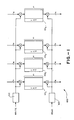
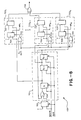
- Fig. 1 is a block diagram of a FIFO memory 100 wherein the present invention is embodied.
- the FIFO memory 100 comprises a plurality, k, of ripple-through FIFO memory arrays, 1011, 1012, 1013,.... 101 k each. Each array has n rows each of which has m bits.
- the input to each of the FIFO memory arrays 101 is controlled by an input control means 102.
- the output of from each FIFO memory array 101 is controlled by an output control means 103.
- Each array 101 has n rows of memory cells. Each row has the same number of memory cells.
- a register or data latches with parallel input can be used to implement a row of memory cells. Data input into a row of cells is controlled by a corresponding flag which provides an enable signal for writing data into the cells.
- Data is input into the top row of an array. When data is written into the top row of an array, it "sinks” towards the bottom and settles into the lowest vacant row.
- FIG. 3 A preferred implementation of the flags is illustrated in Fig. 3.
- the figure shows the first and second flags of a memory array.
- Each flag comprises, in the preferred implementation, three NOR-gates connected at shown.
- the logic state of a flag, i is represented by its output Q i .
- a "high” initialization signal INIT When the FIFO memory is initialized, (e.g.) at power on, a "high" initialization signal INIT will be applied to gate 302, 304,....of each flag.
- the "high” initialization signal INIT causes output Q i of each flag, i, to become “low”.
- the write signal WR is "high”, which in turn will cause the output E1 of gate 301 to become “low”.
- both Q1 and E1 are “low”
- the output Q1 of gate 303 When both Q1 and E1 are “low”, the output Q1 of gate 303 will become “high”, a "high” level Q1 will cause the output E2 of gate 306 to become “low”.
- the initialization signal INIT also causes the output Q2 of gate 304 to become “low”. When both Q2 and E2 are “low”, the output Q2 of 305 will become “high”, and so on. Thus, at initialization, each flag, i, is reset and will have a "low” level output Q i and a “high” level complement output Q i .
- each flag i is used to enable the storage of data into the corresponding i th row of memory cells.
- Fig. 5 illustrates the flags of the last two rows of an array.
- Gate 506 of the last flag, FLAG n has an input connected to a latch 806.
- the data input of latch 806 is tied to a logical "high”.
- the clock input of latch 806 is connected to receive a read signal RD, which goes from "low” to "high” at each read operation.
- the Q n is also used as a "flag empty” signal to clear latch 806. If the bottom row of an array is empty, the "flag empty” ( Q n ) will be high, so that latch 806 will not be set even with the activation of the read signal RD. When a read operation is issued to an empty array, the "flag empty” will be clocked by the read signal RD to generate an "underflow” signal.
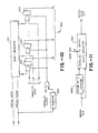
- Fig. 7 is diagram which illustrates a first embodiment of the present invention.
- the inputs of the FIFO memory arrays 101 are coupled together to receive common data input.
- An input control means 102 is provided to sequentially select in a predetermined order, one of the arrays to store data of each of successive input operations.
- the respective output of the memory arrays 101 are coupled together to a common output.
- An output control means 103 is provided to sequentially selects data from one of the arrays as output the the FIFO memory 100 for each of successive output operations.
- the arrays are selected in the same predetermined order as an input operation.
- Fig. 8 an input control means 102 for sequentially selecting, at each input operation, one of the k arrays to store an input data.
- the input control means 102 comprises a state machine 701 that generates k select signals, and k selector drivers 703 each of which receives a different select signal from the state machine 701 to enable input data into one of the k memory arrays.
- the state machine 701 is implemented with a ring counter having k latches, with each latch being clocked at each input operation.
- the latches L1...L k is reset by the initialization signal INIT along with latch 702.
- the negative output of latch 702 will be "high”, which in turn causes a "high” at the output of gate 704.
- the output of gate 704 is clocked into latch L1. Because the input of gate 702 is tied “high” signal, the first write signal will also gate a "high” into latch 702, so that its negative output will return to "low” level.
- one of the latches in 701 will be “high”.
- the "high” level of this latch clocks the latch 706 in one of the select drivers 703 and loads a "high” into the latch.
- the respective negative output of latches 706 of the select drivers are used as the WR signal that go into the first flags of the memory arrays, as previously discussed.
- Latch 706 is reset by either the initialization signal INIT or the output E1 of the first flag of an array. If the top row is not occupied, the "low"-"high”-"low” transition of E1 will reset latch 706 at each input operation.
- latch 706 When the top row is occupied, the E1 signal will remain “low” even when when WR is active, and latch 706 will not be reset. At the next input operation, the "high” level of latch 706 will be clocked into latch 707, causing its output to become “high”. The output of latch 707 is used to generate an "overflow" signal at the output of gate 708.
- the input control means 102 thus sequentially selects one of the arrays 101 to store data of each of successive input operations in a predetermined order.
- k is equal to 3
- one such predetermined order may be array 1, array 2, array 3, array 1, array 2, ... More specifically, data from a first input operation will be written into array 1, data from the next input operation will be written into array 2, then array 3, then array 1, and so on.
- the predetermined order may be array 2, array 3, array 1, array 2, array 3 ...
- Fig. 9 illustrates a logic diagram of a preferred implementation of the output control means 103 for selecting the appropriate output from one of the arrays as the out of the FIFO memory.
- the output control means comprises a ring counter 801, a latch 806 coupled to the counter 801 for generating the CLRFLG signal which clears a corresponding flag upon the removal of data from an array.
- the latch 806 shown in Fig. 6 is the same latch 806 as shown in Fig. 5.
- the counter 801 is coupled to an output driver 803 for gating out the output of one of the array as the output of the FIFO memory 100.
- the ring counter 801 comprises k latches 801, where k corresponds to the number of arrays in the FIFO memory 100.
- the latches 801 are reset to zero at initialization. After initialization, the first latch 801a will be set to "high” by the first read operation. Each read operation causes a "high" signal to ripple in position around in the counter 801.
- the output of the counter 801 enables the output from an array to the data-out terminal of gate 809.
- the output of counter 801 also clocks a latch 806, the output of which is used to clear the last flag of the array being read.
- the output control means 103 thus sequentially selects output from one of the arrays 101 as output of the FIFO memory 100 for each of successive output operations.
- the selection is performed in the same predetermined order as the input control means 102. For example, if the predetermined order of the input control means 102 is array 2, array 3, array 1, array 2, ..., the sequence of arrays selected by the output control means will also be array 2, array 3, array 1, array 2..., and so on.
- Fig. 10 illustrates an optional input interface 900 of the FIFO memory 100 for converting serial input data into parallel output data.
- the interface 900 comprises a shift register 901 for receiving serial data input.
- the shift register 901 is clocked with a "serial" clock every time serial data bit is input.
- Counter 902 being clocked by same "serial clock” signal, keeps track of the number of bits already entered into the shift register 901.
- the counter 902 will load the output of the shift register into latches 903.
- the input interface 900 can also accept parallel data directly into latches 903 if a "parallel clock" signal is applied.
- Fig. 10 illustrates an optional output interface for converting parallel output data from an array to serial output data of the FIFO memory 100.
- the m-bit parallel data enters a m-bit divide-by-m counter.
- the content of the parallel-to-serial shift register 1001 is output by a serial-out-clock.
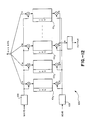
- Fig. 12 illustrates a configuration wherein the FIFO memory 100 are being used as a bus funnel.
- the input control means 102 is implemented so that data from each input operation is stored in parallel in all the arrays.
- the output control means 103 is implemented so that output of the FIFO memory 100 is taken, at each output operation, from one of the arrays based upon a predetermined logic function.
- the logic function is implemented so that the arrays are output sequentially, as provided by the circuit of Fig. 9.
- the FIFO memory 100 of Fig. 12 has four arrays each with eight bits. At each input operation, thirty two bits of input data is simultaneously written into all four arrays. At each output operation, however, only the output of one array is taken.
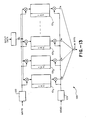
- Fig. 13 illustrates a configuration wherein the FIFO memory 100 are being used as a bus expander.
- the output control means 103 is implemented so that data in the FIFO memory 100 is output in parallel.
- the input controlled means is implemented so that input to the FIFO memory 100 is stored, at each input operation, in one of the arrays based upon a predetermined logic function.
- the logic function is implemented so that the arrays receive input data sequentially, as provided by the circuit of Fig. 8.
- the FIFO memory 100 of Fig. 13 has four arrays each with eight bits. Each input operation only has eight bits of data, and is input into one of the arrays, At each output operation, thirty two bits will be simultaneously taken from the FIFO memory 100.
Abstract
Description
- This invention relates generally to first-in, first-out (FIFO) memories and preferably to a data buffer provided by at least two ripple-through type FIFO memories connected in parallel.
- First-in, first-out (FIFO) memories are versatile devices used in many digital applications as data buffers for allowing intersystem communication in the presence of short term mismatches between the systems' respective data rates. For example, when a central processing unit (CPU) is connected to communicate data with one or more input/output (I/O) devices, the I/O devices typically produce data in asynchronous bursts, but at an average rate that is slower than the capability of the CPU to accept the data. If the CPU is required to be diverted from its main tasks to handle data-ready interrupts from the I/O devices each time a unit of information is sent, its efficiency will be greatly reduced.
- A FIFO memory provides an economical way to alleviate performance degradation due to the above-discussed speed mismatches by providing a buffer between the systems. For example, with a FIFO memory, data generated from an I/O device can be deposited in the FIFO memory, to be retrieved by the CPU at a more convenient time, so that the CPU and the I/O devices can operate with reduced interruptions from each other.
- Two most commonly used FIFO memory architectures are RAM-based FIFOs and ripple-through FIFO memories.
- A RAM-based FIFO memory comprises basically a random access memory, an input counter, and an output counter. The input counter increments sequentially at each data input operation and points to FIFO memory location wherein the next input data is to be deposited. The output counter increments sequentially at each data output operation and points to the FIFO memory location wherefrom the next output data is to be retrieved. Both counters wrap around from the highest address to the zero address. The output counter follows the input counter so that the region from the output counter to the input counter is contained data of the FIFO memory and its complementary region is logically vacant. When the output counter catches up with the input counter, the FIFO memory is empty and output requests are rejected. When the input counter catches up with the output counter, the FIFO memory is full and input requests are rejected. Thus, at each input or output operation, a comparison between the input and output counters must be made to determine before the operation can be performed.
- The RAM-based FIFO memory is structurally simple. However, because of the above described comparison requirement before each operation, a RAM-based FIFO memory suffers from the limitation that an input operation cannot be performed simultaneously with an output operation.
- A ripple-through FIFO memory simulates a queue operation. In the ripple-through FIFO memory architecture, data is input at one (the top) end of the FIFO memory. From there the data "sinks" towards the other (the bottom) end of the FIFO memory and settles at the lowest vacant location. The data continues to ripple down at each output operation until it is retrieved from the FIFO memory at the bottom.
- Although a ripple-through FIFO memory does not have the above discussed comparison requirement of the RAM-based FIFO memory, it has other disadvantages. For example, the duration between the instant when data is input into the top of an empty FIFO memory and the instant when the data can be output from the bottom is generally referred to as the fall through time of the FIFO memory. The fall through time of a FIFO memory is usually an undesirable feature because it represents access delay of input data. Obviously, the fall through time is a function of the size of a FIFO memory.
- We will describe FIFO memory buffer that facilitates data communication between two asynchronous data processing devices.
- We will describe a ripple-through FIFO memory whereby input and output operations can be performed simultaneously.
- We will also describe a ripple-through FIFO memory in which the fall through time is substantially reduced without having to reduce its storage capacity.
- The present invention is ripple-through FIFO memory buffer for facilitating data communication between two asynchronous devices. The FIFO memory buffer according to this invention comprises at least two arrays of ripple-through memory each having an input means and an output means. The FIFO memory buffer according to the present invention has an input control means coupled to each input means for controlling the input to each of the arrays using a first logic function and an output control means coupled each output means for controlling the output from each of the arrays using a second logic function.
- In an embodiment of the present invention, the input control means sequentially selects, at each input operation, one of the arrays to store an input data in accordance with a predetermined order, and the output control means sequentially selects, at each output operation, output from one of the arrays in accordance with the same predetermined order. The advantage provided by this embodiment is a FIFO memory with substantially reduced fall through time.
-
- Fig. 1 is a block diagram of the FIFO memory wherein the present invention is embodied.
- Fig. 2 illustrates the structure of a memory array in the FIFO memory in the embodiment of the present invention.
- Fig. 3 is a schematic logic diagram of the first and second flags of a memory array in the embodiment of the present invention.
- Fig. 4 is a timing diagram illustrating the operation of the flags during a write operation.
- Fig. 5 is a schematic logic diagram of the last and second last flags of a memory array in the embodiment of the present invention.
- Fig. 6 is a timing diagram illustrating the operation of the flags during a read operation.
- Fig. 7 illustrates an embodiment of the present invention wherein fall-through time of a FIFO memory is reduced.
- Fig. 8 is a schematic logic diagram of the input control means for selecting a memory array to store an input data in the embodiment of the present invention.
- Fig. 9 is a schematic logic diagram of the output control means for selecting data from a memory array as the output of the FIFO memory in the embodiment of the present invention.
- Fig. 10 illustrates an input interface for converting serial input data to parallel input data.
- Fig. 11 illustrates an output interface for converting parallel output data to serial output data.
- Fig. 12 illustrates a bus funnel wherein the present invention is embodied.
- Fig. 13 illustrates a bus expander wherein the present invention is embodied.
- Fig. 1 is a block diagram of a
FIFO memory 100 wherein the present invention is embodied. TheFIFO memory 100 comprises a plurality, k, of ripple-through FIFO memory arrays, 101₁, 101₂, 101₃,.... 101k each. Each array has n rows each of which has m bits. The input to each of theFIFO memory arrays 101 is controlled by an input control means 102. The output of from eachFIFO memory array 101 is controlled by an output control means 103. - The structure of one of the
memory arrays 101 is illustrated in Fig. 2. Eacharray 101 has n rows of memory cells. Each row has the same number of memory cells. In actual design, a register or data latches with parallel input can be used to implement a row of memory cells. Data input into a row of cells is controlled by a corresponding flag which provides an enable signal for writing data into the cells. - Data is input into the top row of an array. When data is written into the top row of an array, it "sinks" towards the bottom and settles into the lowest vacant row.
- When data is output from the array, a vacancy is created at the bottom row. The vacancy then "floats" upward. Alternatively stated, when a vacancy is created in an array by an output operation, the data in the upper rows of the array will "sink" to their respective next lower rows. The movement of data within an array is controlled by the flags.
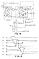
- A preferred implementation of the flags is illustrated in Fig. 3. The figure shows the first and second flags of a memory array. Each flag comprises, in the preferred implementation, three NOR-gates connected at shown.
- The operation of the flags is now described with reference to Fig. 4. The logic state of a flag, i, is represented by its output Qi. When the FIFO memory is initialized, (e.g.) at power on, a "high" initialization signal INIT will be applied to
gate 302, 304,....of each flag. The "high" initialization signal INIT causes output Qi of each flag, i, to become "low". At initialization, the write signalWR is "high", which in turn will cause the output E₁ ofgate 301 to become "low". When both Q₁ and E₁ are "low", the outputQ₁ ofgate 303 will become "high", a "high" levelQ₁ will cause the output E₂ ofgate 306 to become "low". The initialization signal INIT also causes the output Q₂ of gate 304 to become "low". When both Q₂ and E₂ are "low", the outputQ₂ of 305 will become "high", and so on. Thus, at initialization, each flag, i, is reset and will have a "low" level output Qi and a "high" level complement outputQi . - Assume that the top two rows of the memory array are vacant. At each input operation, a "low"
WR signal, as illustrated in Fig. 4a, will appear atgate 301. Because both Q₁ and E₂ are "low", the output E₁ ofgate 301 will become "high", as illustrated in Fig. 4b, onceWR goes "low". A "high" level at the output E₁ ofgate 301 will change the outputQ₁ ofgate 303 to "low", as illustrated in Fig. 4c. The initialization signal INIT is "low" during normal operation of the FIFO memory. When E₂ is "low", a "low"Q₁ will change output Q₁ ofgate 302 from "low" to "high", as illustrated in Fig. 4d. When Q₁ becomes "high", the output E₁ ofgate 301 will go to "low". With a "low" at each of E₁,Q₁ and Q₂, the output E₂ ofgate 306 will become "high", as shown in Fig. 4e. When E₂ goes to a "high", it forces the output Q₁ ofgate 302 to "low". A "high" E₂ also changes the outputQ₂ ofgate 305 to "low", as illustrated in Fig. 4f. It can be seen from Figs. 4b4d that the output Ei of a flag, i, once set, will be reset after three gate delays. Therefore when the outputQ₂ ofgate 305 drops, the output Q₂ of gate 304 will go to "high". Accordingly when a write signalWR appears at the first flag, a "high" signal will ripple through the flags. - The signal Ei of each flag i is used to enable the storage of data into the corresponding ith row of memory cells.
- Assume that when the write signal
WR appears, the second row is already occupied, so that Q₂ ofFLAG 2 is "high". A "high" Q₂ at the input of 306 causes a "low" at E₂, regardless of the level E₁. As a result, the transition of E₂ as shown in Fig. 4E will not occur, and Q₁ will stay at a "high" level. Therefore, when a write signalWR is applied to the flags, it will ripple from the top and stop at the lowest vacant position which in this case is the second row. - Fig. 5 illustrates the flags of the last two rows of an array.
Gate 506 of the last flag, FLAG n, has an input connected to alatch 806. The data input oflatch 806 is tied to a logical "high". The clock input oflatch 806 is connected to receive a read signal RD, which goes from "low" to "high" at each read operation. - Assume that the bottom two rows of the array are occupied with data so that both Qn of FLAG n and Qn1 of FLAG n1 are "high", and
Qn andQn-1 are "low". With reference to the timing diagrams of Fig. 6, when data is read from (the bottom row) the array, a read signal RD, as illustrated in Fig. 6a, will clock thelatch 806. Because the data input oflatch 806 is tied to a "high", the read signal RD will cause signal CLRFLG to go from "low" to "high", as illustrated in Fig. 6b. A "high" CLRFLG signal at gate 504 causes the output Qn of gate 504 to go to a "low", as illustrated in Fig. 6c. - The "high" CLRFLG signal also causes En to go "low". Thus a "low" Qn signal will cause
Qn to go "high". WhenQn-1 goes to "high", it resetslatch 806 and drops the CLRFLG signal. Since Ei for i = 1 on is always "low", as discussed previously, and Qn-1 is "high", when CLRFLG drops, all inputs togate 506 become "low" and the output En ofgate 506 will become "high", as illustrated in Fig. 6e. When En becomes "high", it causes the output Qn-1 ofgate 502 to go to "low". Moreover, a "high" En signal will cause the outputQn atgate 505 to become "low", which in turn will cause Qn to go "high". As a result, FLAG n-1 will be reset, while FLAG n, after being reset, will again be set to a "high" level. - If only the bottom row of the array is occupied, Qn-1 will be "low" and
Qn-1 will be "high". In this case, a "high" to "low" transition at CLRFLG will not cause output En atgate 506 to go from "low" to "high". - The
Qn is also used as a "flag empty" signal toclear latch 806. If the bottom row of an array is empty, the "flag empty" (Qn ) will be high, so thatlatch 806 will not be set even with the activation of the read signal RD. When a read operation is issued to an empty array, the "flag empty" will be clocked by the read signal RD to generate an "underflow" signal. - In summary, when data is read from the bottom row of an array, a vacancy is created. This vacancy then floats upward to the top. In other words, when data is taken out from the bottom row of the array, the data from all the upper rows will fall down to their respective next lower rows.
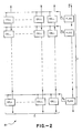
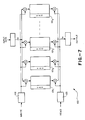
- Fig. 7 is diagram which illustrates a first embodiment of the present invention. In Fig. 7, the inputs of the
FIFO memory arrays 101 are coupled together to receive common data input. An input control means 102 is provided to sequentially select in a predetermined order, one of the arrays to store data of each of successive input operations. The respective output of thememory arrays 101 are coupled together to a common output. An output control means 103 is provided to sequentially selects data from one of the arrays as output the theFIFO memory 100 for each of successive output operations. The arrays are selected in the same predetermined order as an input operation. - In Fig. 8 is shown an input control means 102 for sequentially selecting, at each input operation, one of the k arrays to store an input data. The input control means 102 comprises a
state machine 701 that generates k select signals, and k selector drivers 703 each of which receives a different select signal from thestate machine 701 to enable input data into one of the k memory arrays. - According to the first embodiment, the
state machine 701 is implemented with a ring counter having k latches, with each latch being clocked at each input operation. - With reference to Fig. 8, the latches L₁...Lk is reset by the initialization signal INIT along with
latch 702. After initialization, the negative output oflatch 702 will be "high", which in turn causes a "high" at the output ofgate 704. In a write operation, the output ofgate 704 is clocked into latch L1. Because the input ofgate 702 is tied "high" signal, the first write signal will also gate a "high" intolatch 702, so that its negative output will return to "low" level. - At each write operation, one of the latches in 701 will be "high". The "high" level of this latch clocks the
latch 706 in one of the select drivers 703 and loads a "high" into the latch. The respective negative output oflatches 706 of the select drivers are used as theWR signal that go into the first flags of the memory arrays, as previously discussed. - If the top row of an array is already occupied, Q₁ is "high", so that even if
WR goes from "high" to "low", E₁ will remain "low". -
Latch 706 is reset by either the initialization signal INIT or the output E₁ of the first flag of an array. If the top row is not occupied, the "low"-"high"-"low" transition of E₁ will resetlatch 706 at each input operation. - When the top row is occupied, the E₁ signal will remain "low" even when when
WR is active, and latch 706 will not be reset. At the next input operation, the "high" level oflatch 706 will be clocked intolatch 707, causing its output to become "high". The output oflatch 707 is used to generate an "overflow" signal at the output ofgate 708. - The input control means 102 thus sequentially selects one of the
arrays 101 to store data of each of successive input operations in a predetermined order. As one example, assume k is equal to 3, one such predetermined order may bearray 1,array 2,array 3,array 1,array 2, ... More specifically, data from a first input operation will be written intoarray 1, data from the next input operation will be written intoarray 2, thenarray 3, thenarray 1, and so on. As another example, the predetermined order may bearray 2,array 3,array 1,array 2,array 3 ... - Fig. 9 illustrates a logic diagram of a preferred implementation of the output control means 103 for selecting the appropriate output from one of the arrays as the out of the FIFO memory. The output control means comprises a
ring counter 801, alatch 806 coupled to thecounter 801 for generating the CLRFLG signal which clears a corresponding flag upon the removal of data from an array. In the preferred implementation, thelatch 806 shown in Fig. 6 is thesame latch 806 as shown in Fig. 5. - The
counter 801 is coupled to anoutput driver 803 for gating out the output of one of the array as the output of theFIFO memory 100. Thering counter 801 comprises k latches 801, where k corresponds to the number of arrays in theFIFO memory 100. Thelatches 801 are reset to zero at initialization. After initialization, the first latch 801a will be set to "high" by the first read operation. Each read operation causes a "high" signal to ripple in position around in thecounter 801. The output of thecounter 801 enables the output from an array to the data-out terminal ofgate 809. The output ofcounter 801 also clocks alatch 806, the output of which is used to clear the last flag of the array being read. - As discussed previously in connection with Fig. 5, when a memory array is empty, its
Qn signal (also called "flag empty") will be "high". The "high"Qn signal resets acorresponding latch 806. The output ofcounter 801 is also used to clock a corresponding one of latches 807 the input to latches 807 is a "flag empty" signal. When alatch 801 is "high", an "underflow" signal will be generated fromgate 810. The outputs of acounter 801 are also used to produce the "data ready" signal during a read operation by examining the "read ready" signal from next to be read FIFO memory as shown from Fig. 5. - The output control means 103, thus sequentially selects output from one of the
arrays 101 as output of theFIFO memory 100 for each of successive output operations. The selection is performed in the same predetermined order as the input control means 102. For example, if the predetermined order of the input control means 102 isarray 2,array 3,array 1,array 2, ..., the sequence of arrays selected by the output control means will also bearray 2,array 3,array 1,array 2..., and so on. - Fig. 10 illustrates an
optional input interface 900 of theFIFO memory 100 for converting serial input data into parallel output data. Theinterface 900 comprises ashift register 901 for receiving serial data input. Theshift register 901 is clocked with a "serial" clock every time serial data bit is input.Counter 902, being clocked by same "serial clock" signal, keeps track of the number of bits already entered into theshift register 901. When a predetermined number of serial data bits has entered theshift register 901, thecounter 902 will load the output of the shift register intolatches 903. Theinput interface 900 can also accept parallel data directly intolatches 903 if a "parallel clock" signal is applied. - Fig. 10 illustrates an optional output interface for converting parallel output data from an array to serial output data of the
FIFO memory 100. The m-bit parallel data enters a m-bit divide-by-m counter. the content of the parallel-to-serial shift register 1001 is output by a serial-out-clock. - Fig. 12 illustrates a configuration wherein the
FIFO memory 100 are being used as a bus funnel. In the configuration of Fig. 12, the input control means 102 is implemented so that data from each input operation is stored in parallel in all the arrays. However, The output control means 103 is implemented so that output of theFIFO memory 100 is taken, at each output operation, from one of the arrays based upon a predetermined logic function. - Typically, the logic function is implemented so that the arrays are output sequentially, as provided by the circuit of Fig. 9. By way example, assume that the
FIFO memory 100 of Fig. 12 has four arrays each with eight bits. At each input operation, thirty two bits of input data is simultaneously written into all four arrays. At each output operation, however, only the output of one array is taken. - Fig. 13 illustrates a configuration wherein the
FIFO memory 100 are being used as a bus expander. In the configuration of Fig. 13, the output control means 103 is implemented so that data in theFIFO memory 100 is output in parallel. However, the input controlled means is implemented so that input to theFIFO memory 100 is stored, at each input operation, in one of the arrays based upon a predetermined logic function. - Typically, the logic function is implemented so that the arrays receive input data sequentially, as provided by the circuit of Fig. 8. By way of example, assume that the
FIFO memory 100 of Fig. 13 has four arrays each with eight bits. Each input operation only has eight bits of data, and is input into one of the arrays, At each output operation, thirty two bits will be simultaneously taken from theFIFO memory 100. - While the invention has been particularly shown and described with reference to the referred embodiment, it would be understood by those skilled in the art that changes in form in details could be made therein without departing from the spirit of the invention.
Claims (19)
Applications Claiming Priority (2)
| Application Number | Priority Date | Filing Date | Title |
|---|---|---|---|
| US22715988A | 1988-08-02 | 1988-08-02 | |
| US227159 | 1988-08-02 |
Publications (2)
| Publication Number | Publication Date |
|---|---|
| EP0353942A2 true EP0353942A2 (en) | 1990-02-07 |
| EP0353942A3 EP0353942A3 (en) | 1991-01-16 |
Family
ID=22852003
Family Applications (1)
| Application Number | Title | Priority Date | Filing Date |
|---|---|---|---|
| EP19890307623 Withdrawn EP0353942A3 (en) | 1988-08-02 | 1989-07-27 | A ripple-through fifo memory |
Country Status (2)
| Country | Link |
|---|---|
| EP (1) | EP0353942A3 (en) |
| JP (1) | JPH0298728A (en) |
Cited By (3)
| Publication number | Priority date | Publication date | Assignee | Title |
|---|---|---|---|---|
| GB2265233A (en) * | 1992-03-17 | 1993-09-22 | Fujitsu Ltd | Fifo memory devices |
| WO2000060448A1 (en) * | 1999-03-31 | 2000-10-12 | Koninklijke Philips Electronics N.V. | Data processing arrangement and memory system |
| CN104008770A (en) * | 2013-02-27 | 2014-08-27 | 卡西欧计算机株式会社 | Semi-conductor storing apparatus and data access method |
Citations (3)
| Publication number | Priority date | Publication date | Assignee | Title |
|---|---|---|---|---|
| EP0023568A2 (en) * | 1979-07-30 | 1981-02-11 | International Business Machines Corporation | Data interface mechanism for interfacing bit-parallel data buses of different bit width |
| EP0142263A2 (en) * | 1983-11-10 | 1985-05-22 | Advanced Micro Devices, Inc. | First-in-first-out memory system |
| EP0260897A2 (en) * | 1986-09-16 | 1988-03-23 | Advanced Micro Devices, Inc. | First-in-first-out memory system |
Family Cites Families (4)
| Publication number | Priority date | Publication date | Assignee | Title |
|---|---|---|---|---|
| JPS6111998A (en) * | 1984-06-27 | 1986-01-20 | Nec Corp | Register |
| JPS61112270A (en) * | 1984-11-06 | 1986-05-30 | Oki Electric Ind Co Ltd | Byte converter |
| JPS61127031A (en) * | 1984-11-27 | 1986-06-14 | Fujitsu Ltd | Buffer memory device |
| JPS63168720A (en) * | 1987-01-06 | 1988-07-12 | Toshiba Corp | Memory buffer device |
-
1989
- 1989-07-27 EP EP19890307623 patent/EP0353942A3/en not_active Withdrawn
- 1989-08-01 JP JP1201128A patent/JPH0298728A/en active Pending
Patent Citations (3)
| Publication number | Priority date | Publication date | Assignee | Title |
|---|---|---|---|---|
| EP0023568A2 (en) * | 1979-07-30 | 1981-02-11 | International Business Machines Corporation | Data interface mechanism for interfacing bit-parallel data buses of different bit width |
| EP0142263A2 (en) * | 1983-11-10 | 1985-05-22 | Advanced Micro Devices, Inc. | First-in-first-out memory system |
| EP0260897A2 (en) * | 1986-09-16 | 1988-03-23 | Advanced Micro Devices, Inc. | First-in-first-out memory system |
Non-Patent Citations (1)
| Title |
|---|
| E.D.N. ELECTRICAL DESIGN NEWS, vol. 26, no. 1, 7th January 1981, pages 198,200, Boston, MA, US; M. STOFKA: "Serial/parallel shifts increase RAM speed" * |
Cited By (8)
| Publication number | Priority date | Publication date | Assignee | Title |
|---|---|---|---|---|
| US5515330A (en) * | 1992-01-15 | 1996-05-07 | Fujitsu Limited | FIFO memory device capable of writing contiguous data into rows |
| GB2265233A (en) * | 1992-03-17 | 1993-09-22 | Fujitsu Ltd | Fifo memory devices |
| US5412611A (en) * | 1992-03-17 | 1995-05-02 | Fujitsu, Limited | FIFO memory device capable of writing contiguous data into rows |
| US5513145A (en) * | 1992-03-17 | 1996-04-30 | Fujitsu Limited | FIFO memory device capable of writing contiguous data into rows |
| US5521876A (en) * | 1992-03-17 | 1996-05-28 | Fujitsu Limited | FIFO memory device capable of writing contiguous data into rows |
| GB2265233B (en) * | 1992-03-17 | 1996-10-16 | Fujitsu Ltd | Fifo memory devices |
| WO2000060448A1 (en) * | 1999-03-31 | 2000-10-12 | Koninklijke Philips Electronics N.V. | Data processing arrangement and memory system |
| CN104008770A (en) * | 2013-02-27 | 2014-08-27 | 卡西欧计算机株式会社 | Semi-conductor storing apparatus and data access method |
Also Published As
| Publication number | Publication date |
|---|---|
| JPH0298728A (en) | 1990-04-11 |
| EP0353942A3 (en) | 1991-01-16 |
Similar Documents
| Publication | Publication Date | Title |
|---|---|---|
| US4592019A (en) | Bus oriented LIFO/FIFO memory | |
| US5083269A (en) | Buffer device suitable for asynchronous transfer mode communication | |
| US4646270A (en) | Video graphic dynamic RAM | |
| EP0401340B1 (en) | Method and apparatus for handling high speed data | |
| US5388074A (en) | FIFO memory using single output register | |
| US5490257A (en) | RAM based FIFO memory half-full detection apparatus and method | |
| US4535427A (en) | Control of serial memory | |
| US4825411A (en) | Dual-port memory with asynchronous control of serial data memory transfer | |
| US5587953A (en) | First-in-first-out buffer memory | |
| EP0839354B1 (en) | Memory structure | |
| US4862419A (en) | High speed pointer based first-in-first-out memory | |
| US4642797A (en) | High speed first-in-first-out memory | |
| KR100902765B1 (en) | First-in, first-out memory system and method thereof | |
| US4761732A (en) | Interrupt controller arrangement for mutually exclusive interrupt signals in data processing systems | |
| US4751675A (en) | Memory access circuit with pointer shifting network | |
| EP0166309A2 (en) | Memory chip for a hierarchical memory system | |
| US5157633A (en) | Fifo memory device | |
| US5375208A (en) | Device for managing a plurality of independent queues in a common non-dedicated memory space | |
| US3992699A (en) | First-in/first-out data storage system | |
| EP0520425B1 (en) | Semiconductor memory device | |
| CA2000145C (en) | Data transfer controller | |
| EP0353942A2 (en) | A ripple-through FIFO memory | |
| US5117395A (en) | Expansible FIFO memory for accommodating added memory stages in a multistage memory with common control signals | |
| US5550780A (en) | Two cycle asynchronous FIFO queue | |
| US6289065B1 (en) | FIFO status indicator |
Legal Events
| Date | Code | Title | Description |
|---|---|---|---|
| PUAI | Public reference made under article 153(3) epc to a published international application that has entered the european phase |
Free format text: ORIGINAL CODE: 0009012 |
|
| AK | Designated contracting states |
Kind code of ref document: A2 Designated state(s): AT BE CH DE ES FR GB GR IT LI LU NL SE |
|
| PUAL | Search report despatched |
Free format text: ORIGINAL CODE: 0009013 |
|
| AK | Designated contracting states |
Kind code of ref document: A3 Designated state(s): AT BE CH DE ES FR GB GR IT LI LU NL SE |
|
| 17P | Request for examination filed |
Effective date: 19910418 |
|
| 17Q | First examination report despatched |
Effective date: 19931130 |
|
| STAA | Information on the status of an ep patent application or granted ep patent |
Free format text: STATUS: THE APPLICATION IS DEEMED TO BE WITHDRAWN |
|
| 18D | Application deemed to be withdrawn |
Effective date: 19970718 |