EP0353073B1 - Acoustic surface wave devices - Google Patents
Acoustic surface wave devices Download PDFInfo
- Publication number
- EP0353073B1 EP0353073B1 EP89307660A EP89307660A EP0353073B1 EP 0353073 B1 EP0353073 B1 EP 0353073B1 EP 89307660 A EP89307660 A EP 89307660A EP 89307660 A EP89307660 A EP 89307660A EP 0353073 B1 EP0353073 B1 EP 0353073B1
- Authority
- EP
- European Patent Office
- Prior art keywords
- surface wave
- acoustic surface
- silicon dioxide
- dioxide layer
- substrate
- Prior art date
- Legal status (The legal status is an assumption and is not a legal conclusion. Google has not performed a legal analysis and makes no representation as to the accuracy of the status listed.)
- Expired - Lifetime
Links
Images







Classifications
-
- H—ELECTRICITY
- H03—ELECTRONIC CIRCUITRY
- H03H—IMPEDANCE NETWORKS, e.g. RESONANT CIRCUITS; RESONATORS
- H03H9/00—Networks comprising electromechanical or electro-acoustic elements; Electromechanical resonators
- H03H9/02—Details
- H03H9/02535—Details of surface acoustic wave devices
- H03H9/02818—Means for compensation or elimination of undesirable effects
- H03H9/02834—Means for compensation or elimination of undesirable effects of temperature influence
-
- H—ELECTRICITY
- H03—ELECTRONIC CIRCUITRY
- H03H—IMPEDANCE NETWORKS, e.g. RESONANT CIRCUITS; RESONATORS
- H03H9/00—Networks comprising electromechanical or electro-acoustic elements; Electromechanical resonators
- H03H9/02—Details
- H03H9/02535—Details of surface acoustic wave devices
- H03H9/02543—Characteristics of substrate, e.g. cutting angles
- H03H9/02559—Characteristics of substrate, e.g. cutting angles of lithium niobate or lithium-tantalate substrates
Definitions
- the present invention relates to an acoustic surface wave element, which can be used for a voltage controlled oscillator (VCO), a resonator, a filter, and the like of communication equipment such as a car telephone and a cordless telephone, and of audio equipment such as a video tape recorder (VTR).
- VCO voltage controlled oscillator
- a resonator a filter
- VTR video tape recorder
- an acoustic surface wave element is currently widely used at a frequency of 10 MHz to 1 GHz, and must have a wider frequency deviation range and an excellent stability characteristic to temperature for, for example, a VCO.
- An acoustic surface wave delay line which comprises a substrate of a propagation medium and a surface layer of a medium having a temperature dependent delay time opposite to that of the substrate so that the temperature dependency of the substrate is reduced
- Japanese Unexamined Patent Publication (Kokai) No. 47-37154 published on November 30, 1972.
- This disclosure relates to a general reduction of a temperature dependent delay time of a propagation medium and is exemplified only by a combination of a fused quartz-aluminum.
- the propagation media mentioned are lithium niobate, lithium tantalate, and cadmium sulfide.
- a silicon dioxide layer for the above surface layer has been proposed, to reduce a temperature dependent delay time of propagation media of an acoustic surface wave device (U.S. Patent No. 3,965,444, issued on June 22, 1976).
- piezoelectric materials used for the propagation media there are mentioned YZ-cut lithium niobate and YZ-cut lithium tantalate (col.
- an acoustic surface wave element comprising a combination of SiO2/LiTaO3 (Japanese Unexamined Patent Publication (Kokai) No. 55-159612, published on December 11, 1980).
- This invention uses an X-cut LiTaO3 at an acoustic propagation direction of 112° to the Y-axis.
- This acoustic surface wave element obtained a large electromechanical coupling factor of 1.44%, but this is a small electromechanical coupling factor for an acoustic surface wave element using a single crystal of LiTaO3 and allows only a narrow frequency deviation range for the acoustic surface wave element.
- the electromechanical coupling factor is varied depending on the thickness of the SiO2 layer, and thus it is difficult to manufacture this type of an acoustic surface wave element. Furthermore, a problem arises in that, with an increase of the thickness of the SiO2 layer the inductance component is reduced and the equivalent series resistance is increased, finally resulting in a stopping of the oscillation.
- TCD temperature coefficient of a delay
- Quartz can be used as a substrate of an acoustic surface wave element to obtain not more than 100 ppm of TCD at -20°C to +70°C, but quartz has a very small electromechanical coupling factor and is not suitable for a VCO with a wide frequency deviation range.
- EP-A-0 034 351 discloses an acoustic surface wave device according to the preamble of accompanying claim 1.
- the substrate is X-cut and the direction of propagation is chosen between 80° and 180° measured from the Y-axis toward the Z-axis.
- an acoustic surface wave element comprising:- a substrate of a single crystal lithium tantalate having X, Y and Z crystal axes and a top surface and side walls; electrodes formed on the top surface of the substrate such that an acoustic surface wave is propagated and an oscillation of the acoustic surface wave occurs at a predetermined frequency; and a layer of silicon dioxide covering the electrodes and the substrate; characterised in that:- the substrate is a 36° rotated Y-cut substrate, and the acoustic surface wave is propagated in the direction of the X-axis of the substrate; the electrodes have a thickness equal to 1 to 4% of a wavelength of the acoustic surface wave at the oscillation; and the silicon dioxide layer is deposited by plasma CVD, the silicon dioxide layer having a refractive index of 1.445 to 1.486 and a thickness equal to 16 to 26% of the wavelength of the acoustic surface wave at the oscillation.
- An acoustic surface wave element embodying the present invention is, for example, suitable for oscillation at a frequency in a range of 70 MHz to 1 GHz.
- the following table shows electromechanical coupling factors and temperature coefficients of the oscillation frequency (TCF) of various single crystal substrates.
- the 36° Y-X substrate (cut from a Y-substrate rotated around the X-axis to the Z-axis by 36°) of an LiTaO3 single crystal has a superior coupling factor to that of quartz but an inferior TCF; a superior coupling factor to that of the 112° Y-X substrate of LiTaO3 single crystal but a slightly inferior TCF; and a slightly inferior coupling factor to that of the 128° Y-X substrate of LiNbO3 single crystal but a superior TCF.
- An embodiment of the present invention can provide an efficient and stable acoustic surface wave element by using this 36° Y-X substrate of LiTaO3 single crystal while specifying the thickness of electrodes from a wavelength of the oscillation acoustic surface wave, and depositing a silicon dioxide layer having a thickness specified from the wavelength of the oscillation acoustic surface wave over the electrodes and substrate, by plasma CVD.
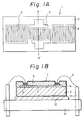
- FIGS 1A and 1B illustrate an acoustic surface wave element embodying the present invention.
- 1 denotes an acoustic surface wave element
- 2 a substrate of 36° Y-X LiTaO3 single crystal
- 3 drive electrodes 4
- reflective electrodes 5
- a silicon dioxide layer 6
- 6 an etching stopper
- 7 an insulator for adjusting an oscillation frequency
- 8 a pyroelectricity preventing film
- 9 wires, 10 take-out pins
- 11 a stem and 12 an adhesive.
- Figure 2 illustrates a substrate 2 of 36° Y-X LiTaO3 single crystal, which has a main surface involving the directions X and Z′ and the right angle to the main surface in the direction of Y′, while the X, Y and Z axes are the crystal axes of the LiTaO3.
- the Y′ axis is rotated around the X axis toward the Z axis by 36°.
- the electrodes 3 and 4 are formed on the main surface of the substrate 2 such that an acoustic surface wave is propagated in the direction of the X axis.
- FIG 3 illustrates a Y-Z substrate cut perpendicularly to the Y axis, i.e., in the plane of the X and Z axes, wherein electrodes are formed on a main surface of the substrate such that an acoustic surface wave is propagated in the direction of the Z axis.
- the drive electrodes 3 are in the form of fingers and the reflective electrodes 4 are in the form of grids, as shown in Fig. 1A.
- the fingers of the drive electrodes 3 and the grids of the reflective electrodes 4 are arranged at a pitch of 1/2 ⁇ (where ⁇ is a wavelength of an acoustic surface wave of a desired oscillation frequency), as shown in Fig. 4A.
- Figure 4B illustrates a previously-considered arrangement of electrodes, in which the pitch between the drive electrodes 3 and the reflective electrodes 4 is 7/8 ⁇ .
- the oscillation frequency is 150 MHz
- the width of the finger and the grid of the electrodes is 6.6 »m and the pitch thereof is 13.2 »m.
- the number of fingers of the drive electrodes is 70 pairs and the number of the grids of the reflective electrodes is 50 pairs.
- the energy of the acoustic surface wave is confined in the substrate and an oscillation is caused by a multiple reflection thereof.
- the oscillation includes substantially no spurious components and the Q value (stability) of the oscillation is improved in comparison with that of the arrangement shown in Fig. 4B.
- Figure 5 shows a capacitance ratio 7, stability Q. and temperature coefficient of the oscillation frequency, of an oscillation in relation to a thickness of electrodes of, in this case, aluminum.
- the width of frequency deviation is wider when the capacitance ratio ⁇ is smaller, and therefore, preferably the capacitance ratio ⁇ is small and the t / ⁇ (where t is thickness of electrodes and ⁇ is wavelength of oscillation acoustic surface wave) is not less than 1%, as seen from the top graph of Fig. 5.
- the stability Q is preferably not less than 500, and therefore, the t/ ⁇ is not more than 4%. From these oscillation characteristics, the thickness of the aluminum electrodes is preferably from 1 to 4% of the t/ ⁇ .
- This graph indicates that not less than 1% of t/ ⁇ is preferably from the view point of an improved efficiency of the temperature coefficient of the oscillation frequency. Therefore, it is clear from the above that the t/ ⁇ (where t is the thickness of the electrodes) is preferably 1 to 4%, more preferably 2% to 3%.
- the materials of the electrodes are not limited to aluminum and include aluminum-silicon alloy (10 wt% or less Si), aluminum-copper alloy (10 wt% or less Cu), aluminum-titanium alloy (10 wt% or less Ti), aluminum-titanium copper alloy (10 wt% or less Ti + Cu), and any of the above-aluminum-alloys/titanium bilayer, etc.
- the electrodes may be formed in any conventional manner, for example, by depositing aluminum and then patterning.
- the silicon dioxide layer is preferably formed by an energy-enhanced chemical vapour deposition method, such as plasma CVD.
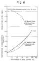
- Figure 6 shows characteristics of an oscillator when the silicon dioxide layer is formed by plasma CVD and by RF magnetron sputtering. As seen in Fig. 6, when the silicon dioxide layer is formed by magnetron sputtering, the oscillation level is lowered and the oscillation stops before the temperature coefficient reaches zero, with an increase of the thickness of the silicon dioxide layer. Therefore, magnetron sputtering is not very efficient for the purpose of the present invention. The differences of layers formed by plasma CVD and RF magnetron sputtering can be easily found from the deposited layer per se and/or the characteristics of the oscillator using the layer.
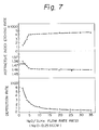
- Figure 7 shows the characteristics of the silicon dioxide layer formed by plasma CVD.
- source gases nitrogen suboxide (N2O) and silane (SiH4) were used.
- the reaction occurred as shown by the following formula: SiH4 + 2N2O -- SiO2 + 2H2 + 2N2
- the flow rate of N2O was constant, 0.25 sccm, and the flow rate ratio between N2O and SiH4 was varied.
- the top graph shows the etching rate, the middle graph the refractive index, and the bottom graph the deposition rate.
- the flow rate ratio of N2O/SiH4 when the flow rate ratio of N2O/SiH4 is less than 5/1, the etching rate is lowered and the refractive index is increased so that the silicon dioxide layer becomes silicon rich. Accordingly, the flow rate ratio of N2O/SiH4 of 5/1 or more was used, even though the deposition rate became low.
- Figure 8 shows the oscillation level and the temperature characteristic of the oscillation frequency in relation to the thickness of the silicon dioxide layer.
- the thickness of the silicon dioxide layer is expressed as T/ ⁇ (where T is a thickness of the silicon dioxide layer and ⁇ is a wavelength of the oscillation acoustic surface wave).
- the temperature characteristic of the oscillation frequency is expressed in the unit "ppm/°C", i.e., difference of oscillation frequency in ppm per change of temperature of 1°C.
- Figure 9 shows the change of the oscillation frequency in relation to temperature at the above zero temperature coefficient.
- the change of the oscillation frequency is excellent and is within 10 ppm at a temperature range of -10°C to +45°C.
- Figure 10 shows the temperature characteristic of the oscillation frequency in relation to the refractive index, in which the solid line A shows the thickness of the silicon dioxide layer obtaining a zero temperature coefficient at a refractive index of 1.46 (at a refractive index of 1.46, the thickness of the silicon dioxide layer obtaining a zero temperature coefficient is minimum), and the broken line B shows the thickness of the silicon dioxide layer obtaining a temperature coefficient of +5 ppm/°C at a refractive index of 1.46. Since the desired temperature characteristic of the oscillation frequency is within ⁇ 3 ppm/°C, the refractive index of the silicon dioxide layer is preferably 1.445 to 1.486, but as seen in Fig.
- a small refractive index of the silicon dioxide layer can be obtained by adjusting the temperature of the substrate during deposition, even though it is difficult to control the temperature of the substrate for a small refractive index, and therefore, a refractive index range of 1.450 to 1.486 is preferable.
- Figure 12 shows a change of the oscillation frequency in relation the thickness of silicon dioxide layer T/ ⁇ , in which the refractive index of the silicon dioxide layer and the thickness of the aluminum electrodes (t) were varied.
- the refractive index is 1.46 and the t/ ⁇ is 4%.
- the refractive index is 1.46 and the t/ ⁇ is 3%.
- the refractive index is 1.46 and the t/ ⁇ is 1%.
- the refractive index is 1.75 and the t/ ⁇ is 3%.
- the thickness of the electrodes is preferably 1% to 4% as the t/ ⁇ , and therefore, when the lines C, D, E and F are seen from this viewpoint, the temperature characteristic of the oscillation frequency is changed with the T/ ⁇ , and thus the T/ ⁇ is preferably 18% to 24% for a temperature coefficient of the oscillation coefficient within ⁇ 5 ppm/°C.
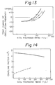
- Figure 13 shows the temperature characteristic of the oscillation frequency in relation to the thickness of the silicon dioxide layer (T/ ⁇ ), in which the dotted line indicates a flow rate ratio of N2O/SiH4 of 5/1, the broken line a flow rate ratio of 10/1, and the solid line a flow rate ratio of 20/1. This figure shows that the temperature characteristic of the oscillation frequency is changed by varying the flow rate ratio of N2O/SiH4.
- Figure 14 shows the electromechanical coupling factor in relation to the ratio of the thickness of the silicon dioxide layer to the oscillation frequency (T/ ⁇ ), in which the solid line indicates a 36° Y-X substrate for use in an embodiment of the invention and the broken line shows a 112° Y-X substrate. It is seen that the change of the electromechanical coupling factor of the 36° Y-X substrate is much smaller than that of the 112° Y-X substrate.
- Figure 15 shows a rate of change of the oscillation frequency in relation to a control voltage, in which the solid line indicates a ratio of the thickness of the silicon dioxide layer to the oscillation frequency (T/ ⁇ ) of 19.5%, the broken line that of 20.0%, and the dotted line that of 20.5%. It is seen that the rate of change of the oscillation frequency of the respective elements is almost linearly changed with the control voltage at a voltage of 5 V or less and the slope of the line is about 0.1%/V.
- the width of the frequency deviation is 900 ppm/V to 1200 ppm/V, which is far wider than that of a 112° Y-X substrate of LiTaO3 of 50 ppm/V to 150 ppm/V; and the temperature coefficient of oscillation frequency is within ⁇ 5 ppm/°C and may be made zero by selecting the thickness of the electrodes and the conditions of the plasma CVD of the silicon dioxide layer.
- the electrodes 3 are electrically connected to an outer circuit through the wires 9 and the pins 10, and the silicon dioxide layer 5 is locally etched so that the wires 9 can be bonded to the electrodes 3.
- the local etching is preferably carried out by wet etching, to ensure that the electrodes 3 are not damaged, but inevitably the electrodes are slightly etched which is not preferable.
- an etching stopper of a metal 6 may be formed before depositing the silicon dioxide layer 5, so that the electrodes 3 are not damaged during the local etching of the silicon dioxide layer 5.
- the metal of the etching stopper 6 may be, for example, chromium, nickel, cobalt etc.
- an insulator is provided for adjusting an oscillation frequency 7 of preferably tantalun pentaoxide.
- the adjustment of the oscillation frequency may be carried out by adjusting the width or thickness of the electrodes, etc., but this is difficult when the patterns of the electrodes are fine.
- an insulation layer 7 is deposited over the silicon dioxide layer 5 at an appropriate thickness after or particularly while measuring or monitoring the oscillation frequency of an element, so that the oscillation frequency is adjusted to a desired frequency. This method of adjusting the oscillation frequency is easy, effective and precise.
- the acoustic velocity is faster in the lithium tantalate than in the silicon dioxide layer and the silicon oxide film in that order, and as a result, the oscillation frequency of the acoustic surface wave element of lithium tantalate is reduced by the presence of the silicon dioxide layer, which is further reduced by the presence of the silicon oxide film.
- the silicon oxide film may be replaced by a film of, for example, tantalun pentaoxide or silicon nitride.
- the surface of the silicon dioxide layer 5 can be etched to increase the oscillation frequency of the element. Therefore, by these methods of adjusting the oscillation frequency, particularly in combination with a simultaneous monitoring of the oscillation frequency, an acoustic surface wave element with a desired oscillation frequency can be obtained.
- Figure 16 shows the oscillation frequency of an acoustic surface wave element with a silicon oxide film formed over the silicon dioxide layer 5 (3.75 »m in thickness) by electron beam evaporation as the insulator 7 for adjusting the oscillation frequency, in relation to the thickness of the silicon oxide film 7. It is seen that, when the silicon oxide film 7 had a thickness of 0.2 »m, the oscillation frequency of the element was reduced from 178.0 MHz to 176.64 MHz (1.36 MHz reduction), and therefore, the oscillation frequency of 177 MHz can be obtained by a silicon oxide film with a thickness of 0.15 »m.
- Figure 17 shows the rate of change of the oscillation frequency of an acoustic surface wave element with a tantalun pentaoxide film as the insulator 7 for adjusting the oscillation frequency, in relation to the thickness of the tantalun pentaoxide film 7.
- the rate of change of the oscillation frequency was about -0.29% when the tantalun pentaoxide film had a thickness of 0.005 »m, and about -0.58% at a thickness of 0.01 »m.
- Figure 18 shows the rate of change of the oscillation frequency of an acoustic surface wave element with a silicon nitride film as the insulator 7 for adjusting the oscillation frequency, in relation to the thickness of the silicon nitride film 7.
- the rate of change of the oscillation frequency was about -0.67% when the silicon nitride film had a thickness of 0.18 »m, and about -1.1% at a thickness of 0.3 »m.
- Figure 19 shows the rate of change of the oscillation frequency of an acoustic surface wave element in which the silicon dioxide layer was etched for adjusting the oscillation frequency, in relation to the time of the etching.
- the etching was carried out by plasma etching in an atmosphere of carbon tetrafluoride, or a mixture of carbon tetrafluoride with an appropriate amount of oxygen, which does not corrode the electrodes and wires for monitoring.
- the samples 1 to 3 were etched under the following different etching conditions:
- the rates of change of the oscillation frequency of an acoustic surface wave element are changed linearly with the etching time.
- the acoustic surface wave element 1 has a pyroelectricity preventing film 8 on the side walls and the bottom surface thereof, according to a preferred embodiment of the present invention.
- Pyroelectricity occurs due to a change of the temperature of a piezoelectric material, and generates electric charges stored on the surfaces of the piezoelectric material; this is undesirable since it may cause discharge and extraordinary oscillation.
- the pyroelectricity preventing film 8 may be made of dielectric materials such as Al2O3 , SiO2 , Ta2O5 , B4C, SiC, TiC, TiO2 , AIN, Si3N4 ; electric conductors such as titanium, chromium, gold; or electrically-conductive resins.
- the surface of the lithium tantalate substrate perpendicular to the X-axis of the lithium tantalate crystal is theoretically free from pyroelectricity, but minor defects may be formed by chipping during dicing, causing extraordinary oscillation, and therefore, that surface is preferably also covered by the pyroelectricity preventing film.
- the top surface of the substrate is already provided with a dielectric layer of the silicon dioxide layer 5 for controlling the temperature characteristic of the element in this embodiment, and therefore, no additional dielectric film for preventing the pyroelectricity is necessary on this surface. Further, no electrically-conductive material should cover this top surface of the substrate because of the electrodes and wires.
- Figure 20A shows the extraordinary oscillation due to pyroelectricity of an acoustic surface wave element without a silicon dioxide layer 5 and a pyroelectricity preventing layer 9, in which the abscissa is the frequency.
- a temperature change schedule as shown in Fig. 21 was applied to the element.
- Figure 20B shows the extraordinary oscillation due to pyroelectricity of an acoustic surface wave element with a silicon dioxide layer 5 but without a pyroelectricity preventing layer 9. It is seen that the extraordinary oscillation due to pyroelectricity was considerably reduced by the silicon dioxide layer 5 but still occurred.
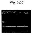
- Figure 20C shows the extraordinary oscillation due to pyroelectricity of an acoustic surface wave element with a silicon dioxide layer 5 and a pyroelectricity preventing layer 9.
- the extraordinary oscillation due to pyroelectricity was completely eliminated by the silicon dioxide layer 5 and the pyroelectricity preventing layer 9.
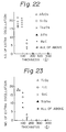
- Figure 22 and 23 show the number of extraordinary oscillations due to pyroelectricity in a predetermined time, of acoustic surface wave elements with a silicon dioxide layer 5 and a pyroelectricity preventing layer 9 of various dielectric materials, in relation to the thickness of the dielectric layer. It is seen that the extraordinary oscillation completely disappeared when the thickness of the dielectric layer was 0.02 »m or more.
Landscapes
- Physics & Mathematics (AREA)
- Acoustics & Sound (AREA)
- Chemical & Material Sciences (AREA)
- Engineering & Computer Science (AREA)
- Materials Engineering (AREA)
- Surface Acoustic Wave Elements And Circuit Networks Thereof (AREA)
Description
- The present invention relates to an acoustic surface wave element, which can be used for a voltage controlled oscillator (VCO), a resonator, a filter, and the like of communication equipment such as a car telephone and a cordless telephone, and of audio equipment such as a video tape recorder (VTR). In the above equipment, an acoustic surface wave element is currently widely used at a frequency of 10 MHz to 1 GHz, and must have a wider frequency deviation range and an excellent stability characteristic to temperature for, for example, a VCO.
- An acoustic surface wave delay line is known which comprises a substrate of a propagation medium and a surface layer of a medium having a temperature dependent delay time opposite to that of the substrate so that the temperature dependency of the substrate is reduced (Japanese Unexamined Patent Publication (Kokai) No. 47-37154, published on November 30, 1972). This disclosure relates to a general reduction of a temperature dependent delay time of a propagation medium and is exemplified only by a combination of a fused quartz-aluminum. The propagation media mentioned are lithium niobate, lithium tantalate, and cadmium sulfide.
- A silicon dioxide layer for the above surface layer has been proposed, to reduce a temperature dependent delay time of propagation media of an acoustic surface wave device (U.S. Patent No. 3,965,444, issued on June 22, 1976). As piezoelectric materials used for the propagation media, there are mentioned YZ-cut lithium niobate and YZ-cut lithium tantalate (col. 4, 1.2-4 of USP′ 444), but such an acoustic surface wave device is difficult to manufacture because, in the case of the YZ-cut lithium tantalate (the acoustic velocity therein is 3230 m/s), at 150 MHz the hK (h = film thickness of the silicon dioxide layer and K = 2π/λ where λ = acoustic wavelength) becomes 3 (col. 4, 1.31-35 of USP′ 444 , and thus the thickness of the silicon dioxide layer must be at least 10.3 »m. A silicon dioxide layer having a thickness of 10 »m causes an increased stress in the layer and a longer deposition time (for example, about 11 hours at a deposition rate of 150 angstroms/min), among other disadvantages.
- Also known is an acoustic surface wave element comprising a combination of SiO₂/LiTaO₃ (Japanese Unexamined Patent Publication (Kokai) No. 55-159612, published on December 11, 1980). This invention uses an X-cut LiTaO₃ at an acoustic propagation direction of 112° to the Y-axis. This acoustic surface wave element obtained a large electromechanical coupling factor of 1.44%, but this is a small electromechanical coupling factor for an acoustic surface wave element using a single crystal of LiTaO₃ and allows only a narrow frequency deviation range for the acoustic surface wave element. Further, the electromechanical coupling factor is varied depending on the thickness of the SiO₂ layer, and thus it is difficult to manufacture this type of an acoustic surface wave element. Furthermore, a problem arises in that, with an increase of the thickness of the SiO₂ layer the inductance component is reduced and the equivalent series resistance is increased, finally resulting in a stopping of the oscillation.
- Further, there is reported a structure of SiO₂/36° Y-X LiTaO₃ for an acoustic surface wave device (W. Chujo et al, "SiO₂/LiTaO₃ , LiNbO₃ Structure Acoustic Surface Wave Materials Fabricated by Plasma CVD Method", Dentsu Gakkai Cho-ompa Kenkyu Shiryo US 80-3, Apr. 1980, pp. 15-20; and W. Chujo et al, "SiO₂/LiTaO₃ , LiNbO₃ Structure Acoustic Surface Wave Materials Fabricated by Plasma CVD Method", Dentsu Gakkai Cho-ompa Kenkyu Shiryo Us 79-16, Jun. 1978, pp 25-30). Here, a zero temperature coefficient of a delay (TCD) is reported at T/λ = 0.11 (T is film thickness of silicon dioxide layer and λ is a wavelength). From experiments by the present inventors, it was found that a relatively thick aluminum layer is necessary to attain a zero TCD at a T/λ (where T is a thickness of the silicon dioxide layer) of about 0.11, and the t/λ (where t is a thickness of an aluminum layer) becomes more than 0.05, lowering the oscillation characteristics.
- Quartz can be used as a substrate of an acoustic surface wave element to obtain not more than 100 ppm of TCD at -20°C to +70°C, but quartz has a very small electromechanical coupling factor and is not suitable for a VCO with a wide frequency deviation range.
- EP-A-0 034 351 discloses an acoustic surface wave device according to the preamble of accompanying
claim 1. The substrate is X-cut and the direction of propagation is chosen between 80° and 180° measured from the Y-axis toward the Z-axis. - According to the present invention there is provided an acoustic surface wave element, comprising:-
a substrate of a single crystal lithium tantalate having X, Y and Z crystal axes and a top surface and side walls;
electrodes formed on the top surface of the substrate such that an acoustic surface wave is propagated and an oscillation of the acoustic surface wave occurs at a predetermined frequency; and
a layer of silicon dioxide covering the electrodes and the substrate;
characterised in that:-
the substrate is a 36° rotated Y-cut substrate, and the acoustic surface wave is propagated in the direction of the X-axis of the substrate;
the electrodes have a thickness equal to 1 to 4% of a wavelength of the acoustic surface wave at the oscillation; and
the silicon dioxide layer is deposited by plasma CVD, the silicon dioxide layer having a refractive index of 1.445 to 1.486 and a thickness equal to 16 to 26% of the wavelength of the acoustic surface wave at the oscillation. - An acoustic surface wave element embodying the present invention is, for example, suitable for oscillation at a frequency in a range of 70 MHz to 1 GHz.
- Figures 1A and 1B are plan and sectional views of an acoustic surface wave element embodying the present invention;
- Fig. 2 shows a 36° rotated Y-cut single crystal lithium tantalate with a propagation of an acoustic surface wave in the X-axis direction;
- Fig. 3 shows a Y-Z substrate;
- Figs. 4A and 4B show respective sectional views of an acoustic surface wave element embodying the present invention. and a previously-considered surface wave element;
- Fig. 5 shows the characteristics of an acoustic surface wave element in relation to the thickness of the electrodes;
- Fig. 6 shows the characteristics of an acoustic surface wave element depending on the methods of forming the silicon dioxide layer;
- Fig. 7 shows the characteristics of the silicon dioxide layer depending on the flow rate ratio of N₂O/SiH₄;
- Fig. 8 shows the characteristics of an acoustic surface wave element in relation to the thickness of the silicon dioxide layer;
- Fig. 9 shows the change of the oscillation frequency in relation to the temperature;
- Fig. 10 shows the temperature characteristic of the oscillation frequency in relation to the refractive index of the silicon dioxide layer;
- Fig. 11 shows the refractive index of the silicon dioxide layer in relation to the temperature of the substrate during the plasma CVD;
- Fig. 12 shows the temperature characteristic of the oscillation frequency in relation to the thickness of the silicon dioxide layer, in which the refractive index of the silicon dioxide layer is changed;
- Fig. 13 shows the temperature characteristic of the oscillation frequency in relation to the thickness of the silicon dioxide layer, in which the flow ratio of N₂O/SiH₄ is changed;
- Fig. 14 shows the electromechanical coupling factor in relation to the thickness of the silicon dioxide layer;
- Fig. 15 shows the rate of change of the oscillation frequency in relation to the control voltage;
- Fig. 16 shows the oscillation frequency in relation to the thickness of the silicon oxide layer;
- Fig. 17 shows the rate of change of the oscillation frequency in relation to the thickness of the tantalun pentaoxide layer;
- Fig. 18 shows the rate of change of the oscillation frequency in relation to the thickness of the silicon nitride layer;
- Fig. 19 shows the rate of change of the oscillation frequency in relation to the etching time of the silicon dioxide layer;
- Figs. 20A to 20C show the extraordinary oscillations of the elements with and without a pyroelectricity preventing film;
- Fig. 21 shows the temperature change schedule for testing the extraordinary oscillations by pyroelectricity; and,
- Figs. 22 and 23 show the number of the extraordinary oscillations by pyroelectricity in relation to the kinds and the thickness of the pyroelectricity preventing films.
- The following table shows electromechanical coupling factors and temperature coefficients of the oscillation frequency (TCF) of various single crystal substrates.

- From the above table it is seen that the 36° Y-X substrate (cut from a Y-substrate rotated around the X-axis to the Z-axis by 36°) of an LiTaO₃ single crystal has a superior coupling factor to that of quartz but an inferior TCF; a superior coupling factor to that of the 112° Y-X substrate of LiTaO₃ single crystal but a slightly inferior TCF; and a slightly inferior coupling factor to that of the 128° Y-X substrate of LiNbO₃ single crystal but a superior TCF. An embodiment of the present invention can provide an efficient and stable acoustic surface wave element by using this 36° Y-X substrate of LiTaO₃ single crystal while specifying the thickness of electrodes from a wavelength of the oscillation acoustic surface wave, and depositing a silicon dioxide layer having a thickness specified from the wavelength of the oscillation acoustic surface wave over the electrodes and substrate, by plasma CVD.
- Figures 1A and 1B illustrate an acoustic surface wave element embodying the present invention. In these figs., 1 denotes an acoustic surface wave element, 2 a substrate of 36° Y-X LiTaO₃ single crystal, 3 drive electrodes, 4 reflective electrodes, 5 a silicon dioxide layer, 6 an etching stopper, 7 an insulator for adjusting an oscillation frequency, 8 a pyroelectricity preventing film, 9 wires, 10 take-out pins, 11 a stem, and 12 an adhesive.
- Figure 2 illustrates a
substrate 2 of 36° Y-X LiTaO₃ single crystal, which has a main surface involving the directions X and Z′ and the right angle to the main surface in the direction of Y′, while the X, Y and Z axes are the crystal axes of the LiTaO₃. As seen in Fig. 2, the Y′ axis is rotated around the X axis toward the Z axis by 36°. Theelectrodes substrate 2 such that an acoustic surface wave is propagated in the direction of the X axis. For reference, Fig. 3 illustrates a Y-Z substrate cut perpendicularly to the Y axis, i.e., in the plane of the X and Z axes, wherein electrodes are formed on a main surface of the substrate such that an acoustic surface wave is propagated in the direction of the Z axis. - The
drive electrodes 3 are in the form of fingers and thereflective electrodes 4 are in the form of grids, as shown in Fig. 1A. The fingers of thedrive electrodes 3 and the grids of thereflective electrodes 4 are arranged at a pitch of 1/2λ (where λ is a wavelength of an acoustic surface wave of a desired oscillation frequency), as shown in Fig. 4A. Figure 4B illustrates a previously-considered arrangement of electrodes, in which the pitch between thedrive electrodes 3 and thereflective electrodes 4 is 7/8λ. For example, when the oscillation frequency is 150 MHz, the width of the finger and the grid of the electrodes is 6.6 »m and the pitch thereof is 13.2 »m. The number of fingers of the drive electrodes is 70 pairs and the number of the grids of the reflective electrodes is 50 pairs. By the arrangement of the electrodes shown in Fig. 4A, the energy of the acoustic surface wave is confined in the substrate and an oscillation is caused by a multiple reflection thereof. The oscillation includes substantially no spurious components and the Q value (stability) of the oscillation is improved in comparison with that of the arrangement shown in Fig. 4B. - Figure 5 shows a
capacitance ratio 7, stability Q. and temperature coefficient of the oscillation frequency, of an oscillation in relation to a thickness of electrodes of, in this case, aluminum. Concerning a VCO, the width of frequency deviation is wider when the capacitance ratio γ is smaller, and therefore, preferably the capacitance ratio γ is small and the t /λ (where t is thickness of electrodes and λ is wavelength of oscillation acoustic surface wave) is not less than 1%, as seen from the top graph of Fig. 5. The stability Q is preferably not less than 500, and therefore, the t/λ is not more than 4%. From these oscillation characteristics, the thickness of the aluminum electrodes is preferably from 1 to 4% of the t/λ. The bottom graph shows the temperature coefficient of the oscillation frequency of the oscillator in relation to the thickness of the electrodes when the thickness of the silicon dioxide layer is adjusted such that the temperature coefficient of the oscillation frequency of the oscillator becomes zero when t/λ = 3% This graph indicates that not less than 1% of t/λ is preferably from the view point of an improved efficiency of the temperature coefficient of the oscillation frequency. Therefore, it is clear from the above that the t/λ (where t is the thickness of the electrodes) is preferably 1 to 4%, more preferably 2% to 3%. - The materials of the electrodes are not limited to aluminum and include aluminum-silicon alloy (10 wt% or less Si), aluminum-copper alloy (10 wt% or less Cu), aluminum-titanium alloy (10 wt% or less Ti), aluminum-titanium copper alloy (10 wt% or less Ti + Cu), and any of the above-aluminum-alloys/titanium bilayer, etc. The electrodes may be formed in any conventional manner, for example, by depositing aluminum and then patterning.
- The silicon dioxide layer is preferably formed by an energy-enhanced chemical vapour deposition method, such as plasma CVD. Figure 6 shows characteristics of an oscillator when the silicon dioxide layer is formed by plasma CVD and by RF magnetron sputtering. As seen in Fig. 6, when the silicon dioxide layer is formed by magnetron sputtering, the oscillation level is lowered and the oscillation stops before the temperature coefficient reaches zero, with an increase of the thickness of the silicon dioxide layer. Therefore, magnetron sputtering is not very efficient for the purpose of the present invention. The differences of layers formed by plasma CVD and RF magnetron sputtering can be easily found from the deposited layer per se and/or the characteristics of the oscillator using the layer.
- Figure 7 shows the characteristics of the silicon dioxide layer formed by plasma CVD. As source gases, nitrogen suboxide (N₂O) and silane (SiH₄) were used. The reaction occurred as shown by the following formula:
SiH₄ + 2N₂O -- SiO₂ + 2H₂ + 2N₂
The flow rate of N₂O was constant, 0.25 sccm, and the flow rate ratio between N₂O and SiH₄ was varied. The top graph shows the etching rate, the middle graph the refractive index, and the bottom graph the deposition rate. In Fig. 7, when the flow rate ratio of N₂O/SiH₄ is less than 5/1, the etching rate is lowered and the refractive index is increased so that the silicon dioxide layer becomes silicon rich. Accordingly, the flow rate ratio of N₂O/SiH₄ of 5/1 or more was used, even though the deposition rate became low. - Figure 8 shows the oscillation level and the temperature characteristic of the oscillation frequency in relation to the thickness of the silicon dioxide layer. The thickness of the silicon dioxide layer is expressed as T/λ (where T is a thickness of the silicon dioxide layer and λ is a wavelength of the oscillation acoustic surface wave). The temperature characteristic of the oscillation frequency is expressed in the unit "ppm/°C", i.e., difference of oscillation frequency in ppm per change of temperature of 1°C. The acoustic surface wave element used for the measurement had aluminum electrodes having a thickness of 3% of λ. It is seen in Fig. 8 that, with a silicon dioxide layer deposited at a flow rate ratio of N₂O/SiH₄ of not less than 5/1 by plasma CVD, substantially no lowering of the oscillation level occurs and a zero temperature coefficient is obtained near T/λ = 20%.
- Figure 9 shows the change of the oscillation frequency in relation to temperature at the above zero temperature coefficient. In Fig. 9, the change of the oscillation frequency is excellent and is within 10 ppm at a temperature range of -10°C to +45°C.
- Figure 10 shows the temperature characteristic of the oscillation frequency in relation to the refractive index, in which the solid line A shows the thickness of the silicon dioxide layer obtaining a zero temperature coefficient at a refractive index of 1.46 (at a refractive index of 1.46, the thickness of the silicon dioxide layer obtaining a zero temperature coefficient is minimum), and the broken line B shows the thickness of the silicon dioxide layer obtaining a temperature coefficient of +5 ppm/°C at a refractive index of 1.46. Since the desired temperature characteristic of the oscillation frequency is within ±3 ppm/°C, the refractive index of the silicon dioxide layer is preferably 1.445 to 1.486, but as seen in Fig. 11, a small refractive index of the silicon dioxide layer can be obtained by adjusting the temperature of the substrate during deposition, even though it is difficult to control the temperature of the substrate for a small refractive index, and therefore, a refractive index range of 1.450 to 1.486 is preferable.
- Figure 12 shows a change of the oscillation frequency in relation the thickness of silicon dioxide layer T/λ, in which the refractive index of the silicon dioxide layer and the thickness of the aluminum electrodes (t) were varied. For the oscillator shown by the solid line C in Fig. 12, the refractive index is 1.46 and the t/λ is 4%. For that shown by the broken line D, the refractive index is 1.46 and the t/λ is 3%. For that shown by the dotted line E, the refractive index is 1.46 and the t/λ is 1%. For that shown by the two-dotted line F, the refractive index is 1.75 and the t/λ is 3%. As described before, the thickness of the electrodes is preferably 1% to 4% as the t/λ, and therefore, when the lines C, D, E and F are seen from this viewpoint, the temperature characteristic of the oscillation frequency is changed with the T/λ, and thus the T/λ is preferably 18% to 24% for a temperature coefficient of the oscillation coefficient within ±5 ppm/°C.
- Figure 13 shows the temperature characteristic of the oscillation frequency in relation to the thickness of the silicon dioxide layer (T/λ), in which the dotted line indicates a flow rate ratio of N₂O/SiH₄ of 5/1, the broken line a flow rate ratio of 10/1, and the solid line a flow rate ratio of 20/1. This figure shows that the temperature characteristic of the oscillation frequency is changed by varying the flow rate ratio of N₂O/SiH₄.
- From the above data, the following conclusions are reached.
- 1) To obtain a zero temperature coefficient of the oscillation frequency at a ratio of the thickness of the electrodes to the oscillation frequency (t/λ) of 1 to 4%, the ratio of the thickness of the silicon dioxide layer to the oscillation frequency (T/λ) is preferably 18% to 24%.
- 2) The deviation of the ratio of the thickness of the silicon dioxide layer to the oscillation frequency (T/λ) is preferably within ±1%, when considering the flow rate ratio of N₂O/SiH₄.
- 3) To suppress the temperature coefficient of the oscillation frequency to within ±5 ppm/°C, the ratio of the thickness of the silicon dioxide layer to the oscillation frequency (T/λ) is preferably 17% to 25%.
- 4) To suppress the temperature coefficient of the oscillation frequency to within ±5 ppm/°C, considering the deviation of the ratio of the thickness of the silicon dioxide layer to the oscillation frequency (T/λ), the ratio of the thickness of the silicon dioxide layer to the oscillation frequency (T/λ) is preferably within 16% to 26%, and the refractive index is preferably 1.455 to 1.486, as described above. A preferable ratio of the thickness of the silicon dioxide layer to the oscillation frequency (T/λ) is within 18% to 22%.
- Figure 14 shows the electromechanical coupling factor in relation to the ratio of the thickness of the silicon dioxide layer to the oscillation frequency (T/λ), in which the solid line indicates a 36° Y-X substrate for use in an embodiment of the invention and the broken line shows a 112° Y-X substrate. It is seen that the change of the electromechanical coupling factor of the 36° Y-X substrate is much smaller than that of the 112° Y-X substrate.
- Figure 15 shows a rate of change of the oscillation frequency in relation to a control voltage, in which the solid line indicates a ratio of the thickness of the silicon dioxide layer to the oscillation frequency (T/λ) of 19.5%, the broken line that of 20.0%, and the dotted line that of 20.5%. It is seen that the rate of change of the oscillation frequency of the respective elements is almost linearly changed with the control voltage at a voltage of 5 V or less and the slope of the line is about 0.1%/V.
- Using a 36° Y-X substrate of LiTaO₃ , for example, in an acoustic surface wave element for a VCO with an oscillation frequency of 155 MHz, the width of the frequency deviation is 900 ppm/V to 1200 ppm/V, which is far wider than that of a 112° Y-X substrate of LiTaO₃ of 50 ppm/V to 150 ppm/V; and the temperature coefficient of oscillation frequency is within ±5 ppm/°C and may be made zero by selecting the thickness of the electrodes and the conditions of the plasma CVD of the silicon dioxide layer.
- Returning to Fig. 1B, the
electrodes 3 are electrically connected to an outer circuit through the wires 9 and thepins 10, and thesilicon dioxide layer 5 is locally etched so that the wires 9 can be bonded to theelectrodes 3. The local etching is preferably carried out by wet etching, to ensure that theelectrodes 3 are not damaged, but inevitably the electrodes are slightly etched which is not preferable. To prevent this unfavorable etching during the local etching of the silicon dioxide layer, an etching stopper of ametal 6 may be formed before depositing thesilicon dioxide layer 5, so that theelectrodes 3 are not damaged during the local etching of thesilicon dioxide layer 5. The metal of theetching stopper 6 may be, for example, chromium, nickel, cobalt etc. - Also in Fig. 1B, an insulator is provided for adjusting an
oscillation frequency 7 of preferably tantalun pentaoxide. The adjustment of the oscillation frequency may be carried out by adjusting the width or thickness of the electrodes, etc., but this is difficult when the patterns of the electrodes are fine. To solve this difficulty, in an embodiment of the present invention, aninsulation layer 7 is deposited over thesilicon dioxide layer 5 at an appropriate thickness after or particularly while measuring or monitoring the oscillation frequency of an element, so that the oscillation frequency is adjusted to a desired frequency. This method of adjusting the oscillation frequency is easy, effective and precise. For example, if a silicon oxide film is deposited over thesilicon dioxide layer 5 by electron beam evaporation, the acoustic velocity is faster in the lithium tantalate than in the silicon dioxide layer and the silicon oxide film in that order, and as a result, the oscillation frequency of the acoustic surface wave element of lithium tantalate is reduced by the presence of the silicon dioxide layer, which is further reduced by the presence of the silicon oxide film. The silicon oxide film may be replaced by a film of, for example, tantalun pentaoxide or silicon nitride. Alternatively, the surface of thesilicon dioxide layer 5 can be etched to increase the oscillation frequency of the element. Therefore, by these methods of adjusting the oscillation frequency, particularly in combination with a simultaneous monitoring of the oscillation frequency, an acoustic surface wave element with a desired oscillation frequency can be obtained. - Figure 16 shows the oscillation frequency of an acoustic surface wave element with a silicon oxide film formed over the silicon dioxide layer 5 (3.75 »m in thickness) by electron beam evaporation as the
insulator 7 for adjusting the oscillation frequency, in relation to the thickness of thesilicon oxide film 7. It is seen that, when thesilicon oxide film 7 had a thickness of 0.2 »m, the oscillation frequency of the element was reduced from 178.0 MHz to 176.64 MHz (1.36 MHz reduction), and therefore, the oscillation frequency of 177 MHz can be obtained by a silicon oxide film with a thickness of 0.15 »m. - Figure 17 shows the rate of change of the oscillation frequency of an acoustic surface wave element with a tantalun pentaoxide film as the
insulator 7 for adjusting the oscillation frequency, in relation to the thickness of the tantalun pentaoxidefilm 7. The rate of change of the oscillation frequency was about -0.29% when the tantalun pentaoxide film had a thickness of 0.005 »m, and about -0.58% at a thickness of 0.01 »m. - Figure 18 shows the rate of change of the oscillation frequency of an acoustic surface wave element with a silicon nitride film as the
insulator 7 for adjusting the oscillation frequency, in relation to the thickness of thesilicon nitride film 7. The rate of change of the oscillation frequency was about -0.67% when the silicon nitride film had a thickness of 0.18 »m, and about -1.1% at a thickness of 0.3 »m. - Figure 19 shows the rate of change of the oscillation frequency of an acoustic surface wave element in which the silicon dioxide layer was etched for adjusting the oscillation frequency, in relation to the time of the etching. The etching was carried out by plasma etching in an atmosphere of carbon tetrafluoride, or a mixture of carbon tetrafluoride with an appropriate amount of oxygen, which does not corrode the electrodes and wires for monitoring. The
samples 1 to 3 were etched under the following different etching conditions:
- The rates of change of the oscillation frequency of an acoustic surface wave element are changed linearly with the etching time.
- Returning to Fig. 1B, the acoustic
surface wave element 1 has apyroelectricity preventing film 8 on the side walls and the bottom surface thereof, according to a preferred embodiment of the present invention. Pyroelectricity occurs due to a change of the temperature of a piezoelectric material, and generates electric charges stored on the surfaces of the piezoelectric material; this is undesirable since it may cause discharge and extraordinary oscillation. Thepyroelectricity preventing film 8 may be made of dielectric materials such as Al₂O₃ , SiO₂ , Ta₂O₅ , B₄C, SiC, TiC, TiO₂ , AIN, Si₃N₄ ; electric conductors such as titanium, chromium, gold; or electrically-conductive resins. The surface of the lithium tantalate substrate perpendicular to the X-axis of the lithium tantalate crystal is theoretically free from pyroelectricity, but minor defects may be formed by chipping during dicing, causing extraordinary oscillation, and therefore, that surface is preferably also covered by the pyroelectricity preventing film. The top surface of the substrate is already provided with a dielectric layer of thesilicon dioxide layer 5 for controlling the temperature characteristic of the element in this embodiment, and therefore, no additional dielectric film for preventing the pyroelectricity is necessary on this surface. Further, no electrically-conductive material should cover this top surface of the substrate because of the electrodes and wires. - Figure 20A shows the extraordinary oscillation due to pyroelectricity of an acoustic surface wave element without a
silicon dioxide layer 5 and a pyroelectricity preventing layer 9, in which the abscissa is the frequency. To examine the extraordinary oscillations due to pyroelectricity, a temperature change schedule as shown in Fig. 21 was applied to the element. Figure 20B shows the extraordinary oscillation due to pyroelectricity of an acoustic surface wave element with asilicon dioxide layer 5 but without a pyroelectricity preventing layer 9. It is seen that the extraordinary oscillation due to pyroelectricity was considerably reduced by thesilicon dioxide layer 5 but still occurred. Figure 20C shows the extraordinary oscillation due to pyroelectricity of an acoustic surface wave element with asilicon dioxide layer 5 and a pyroelectricity preventing layer 9. The extraordinary oscillation due to pyroelectricity was completely eliminated by thesilicon dioxide layer 5 and the pyroelectricity preventing layer 9. - Figure 22 and 23 show the number of extraordinary oscillations due to pyroelectricity in a predetermined time, of acoustic surface wave elements with a
silicon dioxide layer 5 and a pyroelectricity preventing layer 9 of various dielectric materials, in relation to the thickness of the dielectric layer. It is seen that the extraordinary oscillation completely disappeared when the thickness of the dielectric layer was 0.02 »m or more.
Claims (9)
- An acoustic surface wave element, comprising:-
a substrate of a single crystal lithium tantalate having X, Y and Z crystal axes and a top surface and side walls;
electrodes formed on the top surface of the substrate such that an acoustic surface wave is propagated and an oscillation of the acoustic surface wave occurs at a predetermined frequency; and
a layer of silicon dioxide covering the electrodes and the substrate;
characterised in that:-
the substrate is a 36° rotated Y-cut substrate, and the acoustic surface wave is propagated in the direction of the X-axis of the substrate;
the electrodes have a thickness equal to 1 to 4% of a wavelength of the acoustic surface wave at the oscillation; and
the silicon dioxide layer is deposited by plasma CVD, the silicon dioxide layer having a refractive index of 1.445 to 1.486 and a thickness equal to 16 to 26% of the wavelength of the acoustic surface wave at the oscillation. - An acoustic surface wave element according to claim 1, wherein the silicon dioxide layer has a refractive index of 1.450 to 1.486.
- An acoustic surface wave element according to claim 1 or 2, wherein the electrodes have a thickness equal to 2 to 3% of a wavelength of the acoustic surface wave at the oscillation.
- An acoustic surface wave element according to claim 1, 2, or 3, wherein the silicon dioxide layer has a thickness equal to 18 to 22% of the wavelength of the acoustic surface wave at the oscillation.
- An acoustic surface wave element according to any one of claims 1 to 4, having a temperature coefficient of the oscillation frequency of not more than 5 ppm/°C.
- An acoustic surface wave element according to any one of claims 1 to 5, further having an insulator film deposited over the silicon dioxide layer for adjusting the oscillation frequency.
- An acoustic surface wave element according to any one of claims 1 to 6, further having a dielectric layer at least on the side walls of the substrate, for preventing pyroelectricity.
- An acoustic surface wave element according to any one of claims 1 to 7, further having an electric conductor layer at least on the side walls but not on the top surface of the substrate, for preventing pyroelectricity.
- An acoustic surface wave element according to any one of claims 1 to 8, further having an etching stopper of a metal on the electrodes and outer wires connected thereto through windows of the silicon dioxide layer formed on the etching stopper.
Applications Claiming Priority (8)
| Application Number | Priority Date | Filing Date | Title |
|---|---|---|---|
| JP187704/88 | 1988-07-27 | ||
| JP187705/88 | 1988-07-27 | ||
| JP63187704A JPH0748626B2 (en) | 1988-07-27 | 1988-07-27 | Frequency adjustment method for surface acoustic wave device |
| JP63187705A JP2783550B2 (en) | 1988-07-27 | 1988-07-27 | Surface acoustic wave oscillator |
| JP270275/88 | 1988-10-26 | ||
| JP27027588A JPH02116211A (en) | 1988-10-26 | 1988-10-26 | Piezo-electric element |
| JP27676188A JPH02123808A (en) | 1988-11-01 | 1988-11-01 | Manufacture of surface wave device |
| JP276761/88 | 1988-11-01 |
Publications (3)
| Publication Number | Publication Date |
|---|---|
| EP0353073A2 EP0353073A2 (en) | 1990-01-31 |
| EP0353073A3 EP0353073A3 (en) | 1990-09-19 |
| EP0353073B1 true EP0353073B1 (en) | 1995-03-22 |
Family
ID=27475337
Family Applications (1)
| Application Number | Title | Priority Date | Filing Date |
|---|---|---|---|
| EP89307660A Expired - Lifetime EP0353073B1 (en) | 1988-07-27 | 1989-07-27 | Acoustic surface wave devices |
Country Status (3)
| Country | Link |
|---|---|
| US (1) | US4978879A (en) |
| EP (1) | EP0353073B1 (en) |
| DE (1) | DE68921811T2 (en) |
Cited By (1)
| Publication number | Priority date | Publication date | Assignee | Title |
|---|---|---|---|---|
| DE10248444B4 (en) * | 2001-10-17 | 2007-03-22 | Murata Manufacturing Co., Ltd., Nagaokakyo | Surface wave device and method for producing the same |
Families Citing this family (36)
| Publication number | Priority date | Publication date | Assignee | Title |
|---|---|---|---|---|
| US5196753A (en) * | 1989-07-31 | 1993-03-23 | Raytheon Company | Surface acoustic wave devices having long-term frequency stability |
| JPH0468907A (en) * | 1990-07-09 | 1992-03-04 | Kinseki Ltd | Saw electronic component and frequency conversion circuit |
| JPH04358410A (en) * | 1991-06-05 | 1992-12-11 | Sumitomo Electric Ind Ltd | Surface acoustic wave element and production thereof |
| JPH0590864A (en) * | 1991-09-25 | 1993-04-09 | Mitsubishi Materials Corp | Elastic wave device and its manufacture |
| JP2800905B2 (en) * | 1991-10-28 | 1998-09-21 | 富士通株式会社 | Surface acoustic wave filter |
| USRE40036E1 (en) | 1991-10-28 | 2008-01-29 | Fujitsu Limited | Surface acoustic wave filter |
| US5287036A (en) * | 1992-03-02 | 1994-02-15 | Motorola, Inc. | Method and apparatus for acoustic wave inductance |
| TW241397B (en) * | 1993-01-14 | 1995-02-21 | Murata Manufacturing Co | |
| JP3298251B2 (en) * | 1993-08-24 | 2002-07-02 | 株式会社村田製作所 | Surface acoustic wave device |
| JPH07283682A (en) * | 1994-04-13 | 1995-10-27 | Murata Mfg Co Ltd | Surface acoustic wave resonator filter |
| EP0738039B1 (en) * | 1995-04-12 | 2000-06-28 | Matsushita Electric Industrial Co., Ltd. | Resonator ladder surface acoustic wave filter |
| DE59704079D1 (en) * | 1996-05-24 | 2001-08-23 | Epcos Ag | ELECTRONIC COMPONENT, IN PARTICULAR WORKING COMPONENT WITH ACOUSTIC SURFACE WAVES - SAW COMPONENT |
| JPH10276062A (en) * | 1997-03-31 | 1998-10-13 | Sanyo Electric Co Ltd | Surface acoustic wave device |
| JP3391309B2 (en) | 1999-09-02 | 2003-03-31 | 株式会社村田製作所 | Surface wave device and communication device |
| JP2002237736A (en) * | 2001-02-13 | 2002-08-23 | Murata Mfg Co Ltd | Surface acoustic wave device and frequency adjusting method for the device |
| WO2002082644A1 (en) * | 2001-03-30 | 2002-10-17 | Mitsubishi Denki Kabushiki Kaisha | Acoustic wave device and method of manufacture thereof |
| JP3801083B2 (en) * | 2001-06-06 | 2006-07-26 | 株式会社村田製作所 | Surface acoustic wave device |
| JP3945363B2 (en) * | 2001-10-12 | 2007-07-18 | 株式会社村田製作所 | Surface acoustic wave device |
| DE10162540A1 (en) * | 2001-12-19 | 2003-07-10 | Infineon Technologies Ag | Component and method for its production |
| JP3979279B2 (en) * | 2001-12-28 | 2007-09-19 | 株式会社村田製作所 | Surface acoustic wave device |
| JP3780947B2 (en) * | 2002-01-18 | 2006-05-31 | 株式会社村田製作所 | Surface acoustic wave device |
| JP2004254291A (en) * | 2003-01-27 | 2004-09-09 | Murata Mfg Co Ltd | Acoustic surface wave device |
| JP2005176152A (en) * | 2003-12-15 | 2005-06-30 | Alps Electric Co Ltd | Surface acoustic wave element and its manufacturing method |
| WO2005083881A1 (en) * | 2004-03-02 | 2005-09-09 | Murata Manufacturing Co., Ltd. | Surface acoustic wave device |
| KR100804407B1 (en) * | 2004-03-29 | 2008-02-15 | 가부시키가이샤 무라타 세이사쿠쇼 | Manufacturing method of boundary acoustic wave device |
| US7439648B2 (en) * | 2004-08-27 | 2008-10-21 | Kyocera Corporation | Surface acoustic wave device and manufacturing method therefor, and communications equipment |
| DE102004045181B4 (en) | 2004-09-17 | 2016-02-04 | Epcos Ag | SAW device with reduced temperature response and method of manufacture |
| JP2008135971A (en) * | 2006-11-28 | 2008-06-12 | Fujitsu Media Device Kk | Elastic wave device |
| CN101379699B (en) | 2006-12-27 | 2012-04-11 | 松下电器产业株式会社 | Surface acoustic wave resonator, surface acoustic wave filter using the surface acoustic wave resonator, and antenna duplexer |
| CN101868915B (en) * | 2007-11-28 | 2013-11-06 | 株式会社村田制作所 | Elastic wave device |
| CN101911483A (en) * | 2008-01-17 | 2010-12-08 | 株式会社村田制作所 | Surface acoustic wave device |
| WO2009090714A1 (en) * | 2008-01-17 | 2009-07-23 | Murata Manufacturing Co., Ltd. | Surface acoustic wave device |
| US7911111B2 (en) * | 2008-04-15 | 2011-03-22 | Ngk Insulators, Ltd. | Surface acoustic wave devices |
| US8115365B2 (en) * | 2008-04-15 | 2012-02-14 | Ngk Insulators, Ltd. | Surface acoustic wave devices |
| JP2019092019A (en) * | 2017-11-14 | 2019-06-13 | 株式会社村田製作所 | Acoustic wave device, high-frequency front-end circuit, and communication device |
| CN121001553A (en) * | 2025-10-23 | 2025-11-21 | 达波科技(上海)有限公司 | A heterogeneous integrated composite substrate and its preparation method |
Family Cites Families (5)
| Publication number | Priority date | Publication date | Assignee | Title |
|---|---|---|---|---|
| US3786373A (en) * | 1971-10-01 | 1974-01-15 | Raytheon Co | Temperature compensated acoustic surface wave device |
| US3795879A (en) * | 1973-04-04 | 1974-03-05 | Us Navy | Composite dispersive filter |
| US3965444A (en) * | 1975-01-03 | 1976-06-22 | Raytheon Company | Temperature compensated surface acoustic wave devices |
| JPS5930332B2 (en) * | 1979-05-31 | 1984-07-26 | 株式会社東芝 | surface acoustic wave device |
| JPS56116317A (en) * | 1980-02-19 | 1981-09-12 | Matsushita Electric Ind Co Ltd | Material for elastic surface wave |
-
1989
- 1989-07-25 US US07/384,829 patent/US4978879A/en not_active Expired - Lifetime
- 1989-07-27 DE DE68921811T patent/DE68921811T2/en not_active Expired - Fee Related
- 1989-07-27 EP EP89307660A patent/EP0353073B1/en not_active Expired - Lifetime
Cited By (1)
| Publication number | Priority date | Publication date | Assignee | Title |
|---|---|---|---|---|
| DE10248444B4 (en) * | 2001-10-17 | 2007-03-22 | Murata Manufacturing Co., Ltd., Nagaokakyo | Surface wave device and method for producing the same |
Also Published As
| Publication number | Publication date |
|---|---|
| EP0353073A3 (en) | 1990-09-19 |
| US4978879A (en) | 1990-12-18 |
| DE68921811T2 (en) | 1995-07-13 |
| DE68921811D1 (en) | 1995-04-27 |
| EP0353073A2 (en) | 1990-01-31 |
Similar Documents
| Publication | Publication Date | Title |
|---|---|---|
| US4978879A (en) | Acoustic surface wave element | |
| EP0534251B1 (en) | Surface acoustic wave device | |
| US6586861B2 (en) | Film bulk acoustic wave device | |
| US6420820B1 (en) | Acoustic wave resonator and method of operating the same to maintain resonance when subjected to temperature variations | |
| US7230365B2 (en) | Surface acoustic wave apparatus and manufacturing method therefor | |
| US4516049A (en) | Multi-layer acoustic surface wave device having minimal delay time temperature coefficient | |
| KR100200179B1 (en) | Saw apparatus | |
| US7323803B2 (en) | Boundary acoustic wave device | |
| KR101069444B1 (en) | SAS device with improved temperature coefficient | |
| EP0034351B1 (en) | Surface acoustic wave device | |
| EP0392879B1 (en) | Surface acoustic wave device | |
| JPH06164294A (en) | Surface acoustic wave device | |
| EP0657998B1 (en) | Electrode forming method for surface acoustic wave device | |
| JP2783550B2 (en) | Surface acoustic wave oscillator | |
| US6940208B2 (en) | Surface acoustic wave device | |
| US20080111450A1 (en) | Boundary acoustic wave device | |
| US4480209A (en) | Surface acoustic wave device having a specified crystalline orientation | |
| Iriarte et al. | SAW COM-parameter extraction in AlN/diamond layered structures | |
| US5905325A (en) | Optimal cut for saw devices on langanite | |
| JP2005142629A (en) | Surface acoustic wave device and manufacturing method thereof | |
| JP2001044787A (en) | Surface acoustic wave device | |
| EP1056199A2 (en) | Surface acoustic wave device and method of producing the same | |
| JPH05335879A (en) | Surface acoustic wave device | |
| JP3624535B2 (en) | SAW device and manufacturing method thereof | |
| KR20020074484A (en) | Acoustic wave device |
Legal Events
| Date | Code | Title | Description |
|---|---|---|---|
| PUAI | Public reference made under article 153(3) epc to a published international application that has entered the european phase |
Free format text: ORIGINAL CODE: 0009012 |
|
| AK | Designated contracting states |
Kind code of ref document: A2 Designated state(s): DE FR GB NL SE |
|
| PUAL | Search report despatched |
Free format text: ORIGINAL CODE: 0009013 |
|
| AK | Designated contracting states |
Kind code of ref document: A3 Designated state(s): DE FR GB NL SE |
|
| 17P | Request for examination filed |
Effective date: 19901108 |
|
| 17Q | First examination report despatched |
Effective date: 19930811 |
|
| RBV | Designated contracting states (corrected) |
Designated state(s): DE FR SE |
|
| GRAA | (expected) grant |
Free format text: ORIGINAL CODE: 0009210 |
|
| AK | Designated contracting states |
Kind code of ref document: B1 Designated state(s): DE FR SE |
|
| REF | Corresponds to: |
Ref document number: 68921811 Country of ref document: DE Date of ref document: 19950427 |
|
| ET | Fr: translation filed | ||
| PLBE | No opposition filed within time limit |
Free format text: ORIGINAL CODE: 0009261 |
|
| STAA | Information on the status of an ep patent application or granted ep patent |
Free format text: STATUS: NO OPPOSITION FILED WITHIN TIME LIMIT |
|
| 26N | No opposition filed | ||
| PGFP | Annual fee paid to national office [announced via postgrant information from national office to epo] |
Ref country code: SE Payment date: 20030707 Year of fee payment: 15 |
|
| PGFP | Annual fee paid to national office [announced via postgrant information from national office to epo] |
Ref country code: FR Payment date: 20030711 Year of fee payment: 15 |
|
| PGFP | Annual fee paid to national office [announced via postgrant information from national office to epo] |
Ref country code: DE Payment date: 20030807 Year of fee payment: 15 |
|
| PG25 | Lapsed in a contracting state [announced via postgrant information from national office to epo] |
Ref country code: SE Free format text: LAPSE BECAUSE OF NON-PAYMENT OF DUE FEES Effective date: 20040728 |
|
| PG25 | Lapsed in a contracting state [announced via postgrant information from national office to epo] |
Ref country code: DE Free format text: LAPSE BECAUSE OF NON-PAYMENT OF DUE FEES Effective date: 20050201 |
|
| EUG | Se: european patent has lapsed | ||
| PG25 | Lapsed in a contracting state [announced via postgrant information from national office to epo] |
Ref country code: FR Free format text: LAPSE BECAUSE OF NON-PAYMENT OF DUE FEES Effective date: 20050331 |
|
| REG | Reference to a national code |
Ref country code: FR Ref legal event code: ST |