EP0350997B1 - Reactive ion etching of a silicon-bearing material with hydrogen bromide - Google Patents
Reactive ion etching of a silicon-bearing material with hydrogen bromide Download PDFInfo
- Publication number
- EP0350997B1 EP0350997B1 EP89201777A EP89201777A EP0350997B1 EP 0350997 B1 EP0350997 B1 EP 0350997B1 EP 89201777 A EP89201777 A EP 89201777A EP 89201777 A EP89201777 A EP 89201777A EP 0350997 B1 EP0350997 B1 EP 0350997B1
- Authority
- EP
- European Patent Office
- Prior art keywords
- silicon
- etching
- layer
- plasma
- polysilicon
- Prior art date
- Legal status (The legal status is an assumption and is not a legal conclusion. Google has not performed a legal analysis and makes no representation as to the accuracy of the status listed.)
- Expired - Lifetime
Links
Images

Classifications
-
- H—ELECTRICITY
- H10—SEMICONDUCTOR DEVICES; ELECTRIC SOLID-STATE DEVICES NOT OTHERWISE PROVIDED FOR
- H10P—GENERIC PROCESSES OR APPARATUS FOR THE MANUFACTURE OR TREATMENT OF DEVICES COVERED BY CLASS H10
- H10P95/00—Generic processes or apparatus for manufacture or treatments not covered by the other groups of this subclass
-
- H—ELECTRICITY
- H10—SEMICONDUCTOR DEVICES; ELECTRIC SOLID-STATE DEVICES NOT OTHERWISE PROVIDED FOR
- H10P—GENERIC PROCESSES OR APPARATUS FOR THE MANUFACTURE OR TREATMENT OF DEVICES COVERED BY CLASS H10
- H10P50/00—Etching of wafers, substrates or parts of devices
- H10P50/20—Dry etching; Plasma etching; Reactive-ion etching
- H10P50/24—Dry etching; Plasma etching; Reactive-ion etching of semiconductor materials
- H10P50/242—Dry etching; Plasma etching; Reactive-ion etching of semiconductor materials of Group IV materials
-
- H—ELECTRICITY
- H10—SEMICONDUCTOR DEVICES; ELECTRIC SOLID-STATE DEVICES NOT OTHERWISE PROVIDED FOR
- H10P—GENERIC PROCESSES OR APPARATUS FOR THE MANUFACTURE OR TREATMENT OF DEVICES COVERED BY CLASS H10
- H10P50/00—Etching of wafers, substrates or parts of devices
- H10P50/20—Dry etching; Plasma etching; Reactive-ion etching
- H10P50/26—Dry etching; Plasma etching; Reactive-ion etching of conductive or resistive materials
- H10P50/264—Dry etching; Plasma etching; Reactive-ion etching of conductive or resistive materials by chemical means
- H10P50/266—Dry etching; Plasma etching; Reactive-ion etching of conductive or resistive materials by chemical means by vapour etching only
- H10P50/267—Dry etching; Plasma etching; Reactive-ion etching of conductive or resistive materials by chemical means by vapour etching only using plasmas
- H10P50/268—Dry etching; Plasma etching; Reactive-ion etching of conductive or resistive materials by chemical means by vapour etching only using plasmas of silicon-containing layers
Definitions
- the invention relates to a method of manufacturing semiconductor devices by selectively etching a layer of a silicon-bearing material, comprising the steps of
- the silicon-bearing material may be, for example, silicon, polysilicon (both doped and undoped), tantalum silicide or titanium silicide.
- EP-A-272 143 discloses such a method, whereby the silicon-bearing layer is exposed to a plasma formed from a reactive gas mixture comprising as a main etchant gas hydrogen bromide or hydrogen iodide.
- the mixture further comprises SiF 4 , which makes the reaction more volatile, O 2 , which controls the taper and He, which dilutes and reduces black silicon.
- the method is, according to the present invention, characterized in that the silicon-bearing layer is exposed to a plasma formed in an atmosphere of hydrogen bromide alone or hydrogen bromide mixed with an inert gas such as helium, argon or nitrogen.
- a plasma formed in an atmosphere of hydrogen bromide alone or hydrogen bromide mixed with an inert gas such as helium, argon or nitrogen.
- an inert gas such as helium, argon or nitrogen.
- polysilicon can be etched with a selectivity to silicon oxide of 100:1 and a selectivity to photoresist of 60:1.
- the method can be used to produce semiconductor elements for use in IC's having extremely narrow polysilicon lines.
- narrow and deep trenches can be produced in silicon.
- U.S. Patents 4,490,209 and 4,502,915 have considered a two step plasma process for selective anisotropic etching in which an etchant combination of hydrogen chloride, hydrogen bromide, and helium was used. This compound achieves anisotropic etching as a Si-Cl-Br compound in silicon.
- the presently claimed invention seeks to significantly improve reactive ion etching (RIE) of polysilicon using a hydrogen bromide (HBr) plasma for etching polysilicon. It has been found that a hydrogen bromide or HBr plasma significantly improves ion etching of polysilicon and silicon, especially where thin gate oxide layers are present on silicon, and where photo-resist masks are used to selectively etch the polysilicon.
- RIE reactive ion etching
- HBr and Br 2 are significantly better polysilicon or silicon etchants than, for example, Cl 2 .
- Br 2 attacks photoresist by an order of magnitude greater than HBr. That is, the selectivity of etching silicon to photoresist is of the order of 3:1 to 4:1 for Br 2 , while for the etchant HBr of the present invention the etch rate ratio of polysilicon to photo-resist is 60:1.
- This high selectivity for HBr of the present invention applies both to the photoresist and oxide layers, such as the thin gate oxide used in manufacturing IC semiconductor devices.
- the selectivity of etching of polysilicon to oxide is in the ratio of 100:1 for HBr.
- Prior art attempts of etching polysilicon by using Cl 2 only achieve a selectivity of etching of 30:1 relative to oxides. Accordingly, the presently claimed invention provides a significantly improved etching both relative to the oxide and to the photo-resist.
- hydrogen bromide is easier to handle than Br 2 .
- the presently claimed invention provides a significantly improved method of manufacturing semiconductors by selectively etching a layer of a silicon-bearing material using the steps of providing a patterned mask over the layer of silicon-bearing material to expose only areas to be etched, removing any surface oxides from the silicon-bearing layer with an oxide etching plasma, and then exposing the silicon-bearing layer to a hydrogen bromide plasma to selectively etch the silicon-bearing layer relative to photoresist and silicon oxide.
- the silicon-bearing material may be, for example, silicon, polysilicon (both doped and undoped), tantalum silicide or titanium silicide.
- the hydrogen bromide plasma may include HBr gas or HBr gas mixed with an inert gas, such as, for example, He, Ar, or N 2 .
- the oxide etching plasma may be, for example, one of freon, silicon tetrachloride, or boron trichloride. This oxide etching plasma initially removes any surface or native oxides that form on the silicon-bearing material. This vastly improves the etching of the silicon-bearing layer with a HBr plasma.
- Another feature of the present invention is an improved method of manufacturing semiconductor IC components by etching where the steps of forming a composite structure of a silicon substrate with a thin covering layer of oxide on the silicon substrate and a polysilicon layer on the oxide with a photoresist on parts of the polysilicon layer are carried out and further removing any surface from the polysilicon layer with an oxygen-etching-plasma, and then exposing the composite structure to a hydrogen bromide plasma to selectively etch the polysilicon layer relative to the photoresist and the silicon oxide.
- trenches can be produced in silicon with a photoresist mask; and 10 ⁇ m deep trenches can be successfully achieved.
- a reactive ion etcher including a reactor chamber 1.
- a semiconductor wafer 2 is provided in this chamber being mounted on a water cooled electrode 3 which is powered with a RF power source 5, for example.
- the electrode 3 and wafer 2 rest on an insulator structure 4.
- Gas is delivered into the chamber through the entrance 6. Vacuum is maintained by the pump 7.
- An example of this structure may be a Plasma-Therm reactive ion etcher, such as model PK-2480, equipped with a turbo molecular pump.
- Hydrogen bromide gas is provided with a nominal gas flow, for example, of 20 sccm under a pressure of 20 millitorr.
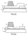
- the semiconductor wafers may be of 100 millimeter diameter having a 5,000 angstrom thick layer of polysilicon 12 on a 500 angstrom thick gate silicon oxide 11, as shown in Figure 2A. These layers are provided on a silicon substrate 10. A layer 13, also of 5,000 angstrom thickness, is also shown which has been previously provided on the silicon dioxide layer 11. This layer 13 may be a previously etched polysilicon layer, i.e., similar to that to be formed from layer 12, or other materials and/or dopings for a semiconductor device.
- photoresist patterns such as pattern 14 is provided on the polysilicon layer 12.
- the photo-resist may be, for example, a patterned Shipley AZ-1470 postbaked to 120°C.
- the photoresist coverages of these patterns may vary, for example only, from 10%, 40%, and 60% of the semiconductor area. Such photoresist coverages can provide various different IC masks.
- the wafer Prior to etching this structure, the wafer is initially exposed to an oxide etching plasma, such as freon, for about 1 minute to clear any negative oxides on the surface of the polysilicon.
- oxide etching plasma such as freon
- Such native oxides can be formed naturally on silicon or polysilicon surfaces just by the presence, for example, of oxygen in the surrounding atmosphere. It has been found that clearing of such oxides from the surface of the silicon or polysilicon layers significantly enhances the ability for HBr etching of silicon and polysilicon.
- Figure 2B shows the semiconductor wafer after etching with a HBr plasma.
- the polysilicon layer 12 is etched completely except under the photoresist 14 where polysilicon 12' remians.
- the photoresist 14 has been minimally or negligibly etched by the HBr plasma.
- the silicon oxide gate layer 11, such as SiO 2 has been slightly etched in the area 11' following removal of overlying layers of the polysilicon 12.
- the thickness of the layer 11 of silicon oxide and the layer 11' While a difference is shown between the thickness of the layer 11 of silicon oxide and the layer 11', this difference is quite small and minimal in view of the fact that any etching of the oxide is significantly smaller than that of the polysilicon.
- the invention effectively provides a high selectivity of etching between the etch rate of the polysilicon to the etch rate of the oxide in amounts of 100:1. This value is significantly more than can be produced with prior etching with Cl 2 .
- a high selectivity of etching between the polysilicon and the photoresist also occurs in that a selectivity ratio of 60:1 between the etch rate of the polysilicon and the etch rate of the photoresist is achieved according to the present invention.
- prior art etching of the photoresist with Cl 2 produces etching of the photoresist with a selectivity of only 3:1, for example.
- the significant difference between the selectivity of etching of the photoresist and the polysilicon according to the present invention from that of the prior art enables extremely fine etching to be carried out in construction of IC devices.
- the etching with HBr is effective with polysilicon layers, as well as monocrystalline silicon layers.
- the polysilicon may be doped such as with phosphorus, for example.
- the HBr plasma thus anisotropically etches polysilicon or single crystal silicon with extremely high selectivity to silicon dioxides and photoresist.
- photoresists may be Shipley AZ-1470 or Kodak -809 photoresist.
- the plasma etching process thus meets all basic requirements for pattern transfer, such as anisotropic profile, good photoresist integrity, high selectivity to underlayer, and freedom of polymers.
- the hydrogen bromide plasma may include HBr gas mixed with an inert gas, such as He, Ar, or N 2 .
- the hydrogen bromide plasma is a much more suitable polysilicon etchant because of (a) the lateral etch rate is very low in the HBr plasma since the reaction probability of Si with atomic Br and thermal energies is a factor of 10 lower than that with Cl, for example, (b) plasma-enhanced polysilicon etch rates in HBr plasmas is compatible with that in chlorinated plasmas since the reaction rate is greater enhanced by Br ion bombardment (> 10 4 ) at 100 eV, compared to that by Cl ion ( ⁇ 10 4 ), (c) the intrinsic oxide etch rate in the HBr plasma is at least a factor of 2 lower than that in chlorinated plasmas, and (d) photoresist etch rates in HBr plasmas is a factor of 10 lower than that in chlorinated plasmas.
Landscapes
- Drying Of Semiconductors (AREA)
Description
Claims (3)
- A method of manufacturing semiconductor devices by selectively etching a layer of a silicon-bearing material, comprising the steps ofproviding a patterned photoresist mask over a layer of silicon-bearing material to expose only areas to be etched,removing any surface oxides from said silicon-bearing layer with an oxide etching plasma and thenexposing said silicon-bearing layer to a plasma formed in an atmosphere of hydrogen bromide alone or hydrogen bromide mixed with an inert gas such as helium, argon or nitrogen, to selectively etch said silicon-bearing layer relative to photoresist and silicon oxide.
- A method according to claim 1, wherein said silicon-bearing material is one of silicon, doped or undoped polysilicon, tantalum silicide or titanium silicide.
- A method according to claim 1, wherein said oxide etching plasma is one of freon, silicon tetrachloride or borontrichloride.
Applications Claiming Priority (2)
| Application Number | Priority Date | Filing Date | Title |
|---|---|---|---|
| US217536 | 1988-07-11 | ||
| US07/217,536 US5007982A (en) | 1988-07-11 | 1988-07-11 | Reactive ion etching of silicon with hydrogen bromide |
Publications (3)
| Publication Number | Publication Date |
|---|---|
| EP0350997A2 EP0350997A2 (en) | 1990-01-17 |
| EP0350997A3 EP0350997A3 (en) | 1990-04-11 |
| EP0350997B1 true EP0350997B1 (en) | 1998-10-07 |
Family
ID=22811475
Family Applications (1)
| Application Number | Title | Priority Date | Filing Date |
|---|---|---|---|
| EP89201777A Expired - Lifetime EP0350997B1 (en) | 1988-07-11 | 1989-07-05 | Reactive ion etching of a silicon-bearing material with hydrogen bromide |
Country Status (5)
| Country | Link |
|---|---|
| US (1) | US5007982A (en) |
| EP (1) | EP0350997B1 (en) |
| JP (1) | JPH0670989B2 (en) |
| KR (1) | KR0185372B1 (en) |
| DE (1) | DE68928826T2 (en) |
Families Citing this family (46)
| Publication number | Priority date | Publication date | Assignee | Title |
|---|---|---|---|---|
| ATE177877T1 (en) * | 1986-12-19 | 1999-04-15 | Applied Materials Inc | BROMINE ETCHING PROCESS FOR SILICON |
| US5316616A (en) * | 1988-02-09 | 1994-05-31 | Fujitsu Limited | Dry etching with hydrogen bromide or bromine |
| EP0439101B1 (en) * | 1990-01-22 | 1997-05-21 | Sony Corporation | Dry etching method |
| JP2577488B2 (en) * | 1990-05-18 | 1997-01-29 | 株式会社東芝 | Method for manufacturing semiconductor device |
| JPH0496223A (en) * | 1990-08-03 | 1992-03-27 | Fujitsu Ltd | Manufacture of semiconductor device |
| JP3127454B2 (en) * | 1990-08-08 | 2001-01-22 | ソニー株式会社 | Etching method of silicon-based material to be etched |
| JPH0779102B2 (en) * | 1990-08-23 | 1995-08-23 | 富士通株式会社 | Method for manufacturing semiconductor device |
| JP3004699B2 (en) * | 1990-09-07 | 2000-01-31 | 東京エレクトロン株式会社 | Plasma processing method |
| US5242536A (en) * | 1990-12-20 | 1993-09-07 | Lsi Logic Corporation | Anisotropic polysilicon etching process |
| US5160407A (en) * | 1991-01-02 | 1992-11-03 | Applied Materials, Inc. | Low pressure anisotropic etch process for tantalum silicide or titanium silicide layer formed over polysilicon layer deposited on silicon oxide layer on semiconductor wafer |
| US5167762A (en) * | 1991-01-02 | 1992-12-01 | Micron Technology, Inc. | Anisotropic etch method |
| JP2920848B2 (en) * | 1991-03-19 | 1999-07-19 | 東京エレクトロン株式会社 | Silicon layer etching method |
| US5560804A (en) * | 1991-03-19 | 1996-10-01 | Tokyo Electron Limited | Etching method for silicon containing layer |
| JP3088178B2 (en) * | 1991-04-22 | 2000-09-18 | 日本電気株式会社 | Polysilicon film etching method |
| US5314573A (en) * | 1991-05-20 | 1994-05-24 | Tokyo Electron Limited | Dry etching polysilicon using a bromine-containing gas |
| JP3179872B2 (en) * | 1991-12-19 | 2001-06-25 | 東京エレクトロン株式会社 | Etching method |
| JP2903884B2 (en) * | 1992-07-10 | 1999-06-14 | ヤマハ株式会社 | Semiconductor device manufacturing method |
| US5286337A (en) * | 1993-01-25 | 1994-02-15 | North American Philips Corporation | Reactive ion etching or indium tin oxide |
| JP3318801B2 (en) * | 1993-12-29 | 2002-08-26 | ソニー株式会社 | Dry etching method |
| US5670018A (en) * | 1995-04-27 | 1997-09-23 | Siemens Aktiengesellschaft | Isotropic silicon etch process that is highly selective to tungsten |
| US5705433A (en) * | 1995-08-24 | 1998-01-06 | Applied Materials, Inc. | Etching silicon-containing materials by use of silicon-containing compounds |
| US5550085A (en) * | 1995-09-07 | 1996-08-27 | Winbond Electronics Corp. | Method for making a buried contact |
| US6253704B1 (en) | 1995-10-13 | 2001-07-03 | Mattson Technology, Inc. | Apparatus and method for pulsed plasma processing of a semiconductor substrate |
| US6794301B2 (en) | 1995-10-13 | 2004-09-21 | Mattson Technology, Inc. | Pulsed plasma processing of semiconductor substrates |
| US5983828A (en) * | 1995-10-13 | 1999-11-16 | Mattson Technology, Inc. | Apparatus and method for pulsed plasma processing of a semiconductor substrate |
| US6451706B1 (en) * | 1996-06-03 | 2002-09-17 | Chartered Semiconductor Manufacturing Ltd. | Attenuation of reflecting lights by surface treatment |
| US5736418A (en) * | 1996-06-07 | 1998-04-07 | Lsi Logic Corporation | Method for fabricating a field effect transistor using microtrenches to control hot electron effects |
| US5843226A (en) * | 1996-07-16 | 1998-12-01 | Applied Materials, Inc. | Etch process for single crystal silicon |
| GB9616225D0 (en) | 1996-08-01 | 1996-09-11 | Surface Tech Sys Ltd | Method of surface treatment of semiconductor substrates |
| DE69725245T2 (en) * | 1996-08-01 | 2004-08-12 | Surface Technoloy Systems Plc | Process for etching substrates |
| US5798303A (en) * | 1996-09-05 | 1998-08-25 | Micron Technology, Inc. | Etching method for use in fabrication of semiconductor devices |
| US6187685B1 (en) | 1997-08-01 | 2001-02-13 | Surface Technology Systems Limited | Method and apparatus for etching a substrate |
| US6083815A (en) * | 1998-04-27 | 2000-07-04 | Taiwan Semiconductor Manufacturing Company | Method of gate etching with thin gate oxide |
| US6417013B1 (en) | 1999-01-29 | 2002-07-09 | Plasma-Therm, Inc. | Morphed processing of semiconductor devices |
| US6340603B1 (en) * | 2000-01-27 | 2002-01-22 | Advanced Micro Devices, Inc. | Plasma emission detection during lateral processing of photoresist mask |
| US6358859B1 (en) * | 2000-05-26 | 2002-03-19 | Taiwan Semiconductor Manufacturing Company | HBr silicon etching process |
| US6402301B1 (en) | 2000-10-27 | 2002-06-11 | Lexmark International, Inc | Ink jet printheads and methods therefor |
| DE10226603A1 (en) * | 2002-06-14 | 2004-01-08 | Infineon Technologies Ag | Method for structuring a silicon layer and its use for producing an integrated semiconductor circuit |
| DE10226604B4 (en) * | 2002-06-14 | 2006-06-01 | Infineon Technologies Ag | Method for structuring a layer |
| US7029958B2 (en) * | 2003-11-04 | 2006-04-18 | Advanced Micro Devices, Inc. | Self aligned damascene gate |
| US8034153B2 (en) * | 2005-12-22 | 2011-10-11 | Momentive Performances Materials, Inc. | Wear resistant low friction coating composition, coated components, and method for coating thereof |
| KR100780832B1 (en) * | 2006-08-16 | 2007-11-30 | 인하대학교 산학협력단 | Dry etching method for zinc oxide |
| JP2010508167A (en) * | 2006-10-31 | 2010-03-18 | アイメック | Manufacturing method of micromachine device |
| JP5537324B2 (en) * | 2010-08-05 | 2014-07-02 | 株式会社東芝 | Manufacturing method of semiconductor device |
| CN109659222B (en) | 2017-10-10 | 2020-10-27 | 联华电子股份有限公司 | Method for forming semiconductor device |
| CN119432382A (en) * | 2024-09-24 | 2025-02-14 | 湖北兴福电子材料股份有限公司 | Polysilicon etching solution |
Family Cites Families (11)
| Publication number | Priority date | Publication date | Assignee | Title |
|---|---|---|---|---|
| JPS5814507B2 (en) * | 1975-07-09 | 1983-03-19 | インタ−ナショナル ビジネス マシ−ンズ コ−ポレ−ション | Method for selectively ion etching silicon |
| US4432132A (en) * | 1981-12-07 | 1984-02-21 | Bell Telephone Laboratories, Incorporated | Formation of sidewall oxide layers by reactive oxygen ion etching to define submicron features |
| US4450042A (en) * | 1982-07-06 | 1984-05-22 | Texas Instruments Incorporated | Plasma etch chemistry for anisotropic etching of silicon |
| JPS58100684A (en) * | 1982-11-26 | 1983-06-15 | Nippon Telegr & Teleph Corp <Ntt> | Dry etching method |
| US4490209B2 (en) * | 1983-12-27 | 2000-12-19 | Texas Instruments Inc | Plasma etching using hydrogen bromide addition |
| US4502915B1 (en) * | 1984-01-23 | 1998-11-03 | Texas Instruments Inc | Two-step plasma process for selective anisotropic etching of polycrystalline silicon without leaving residue |
| US4784720A (en) * | 1985-05-03 | 1988-11-15 | Texas Instruments Incorporated | Trench etch process for a single-wafer RIE dry etch reactor |
| US4702795A (en) * | 1985-05-03 | 1987-10-27 | Texas Instruments Incorporated | Trench etch process |
| JPS62202523A (en) * | 1986-02-28 | 1987-09-07 | Nec Corp | Manufacture of semiconductor device |
| ATE177877T1 (en) * | 1986-12-19 | 1999-04-15 | Applied Materials Inc | BROMINE ETCHING PROCESS FOR SILICON |
| US4778563A (en) * | 1987-03-26 | 1988-10-18 | Applied Materials, Inc. | Materials and methods for etching tungsten polycides using silicide as a mask |
-
1988
- 1988-07-11 US US07/217,536 patent/US5007982A/en not_active Expired - Lifetime
-
1989
- 1989-07-05 EP EP89201777A patent/EP0350997B1/en not_active Expired - Lifetime
- 1989-07-05 DE DE68928826T patent/DE68928826T2/en not_active Expired - Lifetime
- 1989-07-10 KR KR1019890009781A patent/KR0185372B1/en not_active Expired - Fee Related
- 1989-07-10 JP JP1175756A patent/JPH0670989B2/en not_active Expired - Lifetime
Also Published As
| Publication number | Publication date |
|---|---|
| KR0185372B1 (en) | 1999-04-15 |
| KR900002415A (en) | 1990-02-28 |
| JPH0286126A (en) | 1990-03-27 |
| US5007982A (en) | 1991-04-16 |
| JPH0670989B2 (en) | 1994-09-07 |
| DE68928826T2 (en) | 1999-05-12 |
| EP0350997A3 (en) | 1990-04-11 |
| DE68928826D1 (en) | 1998-11-12 |
| EP0350997A2 (en) | 1990-01-17 |
Similar Documents
| Publication | Publication Date | Title |
|---|---|---|
| US5007982A (en) | Reactive ion etching of silicon with hydrogen bromide | |
| US6569773B1 (en) | Method for anisotropic plasma-chemical dry etching of silicon nitride layers using a gas mixture containing fluorine | |
| EP0368732B1 (en) | Process for forming resist mask pattern | |
| JP4466651B2 (en) | Masking method | |
| JP2915807B2 (en) | Etching of molybdenum silicide using sulfur hexafluoride, hydrogen bromide and oxygen | |
| US5338398A (en) | Tungsten silicide etch process selective to photoresist and oxide | |
| US5872061A (en) | Plasma etch method for forming residue free fluorine containing plasma etched layers | |
| EP0814500B1 (en) | Method for etching polycide structures | |
| EP0122776A2 (en) | Dry etching aluminum or aluminum alloy layer | |
| EP0439101B1 (en) | Dry etching method | |
| KR20030066673A (en) | Method of etching tungsten or tungsten nitride electrode gates in semiconductor structures | |
| US5354421A (en) | Dry etching method | |
| WO2003007344A2 (en) | Etch pattern definition using a cvd organic layer as an anti-reflection coating and hardmask | |
| US5651856A (en) | Selective etch process | |
| US5387312A (en) | High selective nitride etch | |
| JPH1098029A (en) | Processing method to etch organic anti-reflective coating from substrate | |
| JP4436466B2 (en) | Etching method | |
| US6069087A (en) | Highly selective dry etching process | |
| US5338395A (en) | Method for enhancing etch uniformity useful in etching submicron nitride features | |
| US7091081B2 (en) | Method for patterning a semiconductor region | |
| US6429140B1 (en) | Method of etching of photoresist layer | |
| US6051502A (en) | Methods of forming conductive components and methods of forming conductive lines | |
| US6531265B2 (en) | Method to planarize semiconductor surface | |
| Sato et al. | Control of etching-product-dependent shape and selectivity in gate polysilicon reactive ion etching | |
| JP2876649B2 (en) | Dry etching method |
Legal Events
| Date | Code | Title | Description |
|---|---|---|---|
| PUAI | Public reference made under article 153(3) epc to a published international application that has entered the european phase |
Free format text: ORIGINAL CODE: 0009012 |
|
| AK | Designated contracting states |
Kind code of ref document: A2 Designated state(s): DE FR GB IT NL |
|
| PUAL | Search report despatched |
Free format text: ORIGINAL CODE: 0009013 |
|
| AK | Designated contracting states |
Kind code of ref document: A3 Designated state(s): DE FR GB IT NL |
|
| 17P | Request for examination filed |
Effective date: 19901009 |
|
| 17Q | First examination report despatched |
Effective date: 19930621 |
|
| APAB | Appeal dossier modified |
Free format text: ORIGINAL CODE: EPIDOS NOAPE |
|
| GRAG | Despatch of communication of intention to grant |
Free format text: ORIGINAL CODE: EPIDOS AGRA |
|
| GRAH | Despatch of communication of intention to grant a patent |
Free format text: ORIGINAL CODE: EPIDOS IGRA |
|
| GRAG | Despatch of communication of intention to grant |
Free format text: ORIGINAL CODE: EPIDOS AGRA |
|
| GRAG | Despatch of communication of intention to grant |
Free format text: ORIGINAL CODE: EPIDOS AGRA |
|
| GRAH | Despatch of communication of intention to grant a patent |
Free format text: ORIGINAL CODE: EPIDOS IGRA |
|
| GRAA | (expected) grant |
Free format text: ORIGINAL CODE: 0009210 |
|
| RAP3 | Party data changed (applicant data changed or rights of an application transferred) |
Owner name: KONINKLIJKE PHILIPS ELECTRONICS N.V. |
|
| AK | Designated contracting states |
Kind code of ref document: B1 Designated state(s): DE FR GB IT NL |
|
| PG25 | Lapsed in a contracting state [announced via postgrant information from national office to epo] |
Ref country code: NL Free format text: LAPSE BECAUSE OF FAILURE TO SUBMIT A TRANSLATION OF THE DESCRIPTION OR TO PAY THE FEE WITHIN THE PRESCRIBED TIME-LIMIT Effective date: 19981007 |
|
| REF | Corresponds to: |
Ref document number: 68928826 Country of ref document: DE Date of ref document: 19981112 |
|
| ET | Fr: translation filed | ||
| NLV1 | Nl: lapsed or annulled due to failure to fulfill the requirements of art. 29p and 29m of the patents act | ||
| PLBE | No opposition filed within time limit |
Free format text: ORIGINAL CODE: 0009261 |
|
| STAA | Information on the status of an ep patent application or granted ep patent |
Free format text: STATUS: NO OPPOSITION FILED WITHIN TIME LIMIT |
|
| 26N | No opposition filed | ||
| REG | Reference to a national code |
Ref country code: GB Ref legal event code: IF02 |
|
| REG | Reference to a national code |
Ref country code: FR Ref legal event code: D6 |
|
| REG | Reference to a national code |
Ref country code: GB Ref legal event code: 746 Effective date: 20021205 |
|
| APAH | Appeal reference modified |
Free format text: ORIGINAL CODE: EPIDOSCREFNO |
|
| REG | Reference to a national code |
Ref country code: GB Ref legal event code: 732E |
|
| REG | Reference to a national code |
Ref country code: GB Ref legal event code: 732E |
|
| REG | Reference to a national code |
Ref country code: FR Ref legal event code: TP |
|
| REG | Reference to a national code |
Ref country code: FR Ref legal event code: GC |
|
| PGFP | Annual fee paid to national office [announced via postgrant information from national office to epo] |
Ref country code: DE Payment date: 20080711 Year of fee payment: 20 |
|
| PGFP | Annual fee paid to national office [announced via postgrant information from national office to epo] |
Ref country code: FR Payment date: 20080718 Year of fee payment: 20 Ref country code: IT Payment date: 20080730 Year of fee payment: 20 |
|
| PGFP | Annual fee paid to national office [announced via postgrant information from national office to epo] |
Ref country code: GB Payment date: 20080709 Year of fee payment: 20 |
|
| REG | Reference to a national code |
Ref country code: GB Ref legal event code: PE20 Expiry date: 20090704 |
|
| PG25 | Lapsed in a contracting state [announced via postgrant information from national office to epo] |
Ref country code: GB Free format text: LAPSE BECAUSE OF EXPIRATION OF PROTECTION Effective date: 20090704 |