EP0337331A1 - Method for producing an allround-shielded transmission line - Google Patents
Method for producing an allround-shielded transmission line Download PDFInfo
- Publication number
- EP0337331A1 EP0337331A1 EP89106223A EP89106223A EP0337331A1 EP 0337331 A1 EP0337331 A1 EP 0337331A1 EP 89106223 A EP89106223 A EP 89106223A EP 89106223 A EP89106223 A EP 89106223A EP 0337331 A1 EP0337331 A1 EP 0337331A1
- Authority
- EP
- European Patent Office
- Prior art keywords
- copper
- film
- areas
- conductive layer
- signal line
- Prior art date
- Legal status (The legal status is an assumption and is not a legal conclusion. Google has not performed a legal analysis and makes no representation as to the accuracy of the status listed.)
- Granted
Links
Images
Classifications
-
- H—ELECTRICITY
- H05—ELECTRIC TECHNIQUES NOT OTHERWISE PROVIDED FOR
- H05K—PRINTED CIRCUITS; CASINGS OR CONSTRUCTIONAL DETAILS OF ELECTRIC APPARATUS; MANUFACTURE OF ASSEMBLAGES OF ELECTRICAL COMPONENTS
- H05K1/00—Printed circuits
- H05K1/02—Details
- H05K1/0213—Electrical arrangements not otherwise provided for
- H05K1/0216—Reduction of cross-talk, noise or electromagnetic interference
- H05K1/0218—Reduction of cross-talk, noise or electromagnetic interference by printed shielding conductors, ground planes or power plane
- H05K1/0219—Printed shielding conductors for shielding around or between signal conductors, e.g. coplanar or coaxial printed shielding conductors
- H05K1/0221—Coaxially shielded signal lines comprising a continuous shielding layer partially or wholly surrounding the signal lines
-
- H—ELECTRICITY
- H01—ELECTRIC ELEMENTS
- H01P—WAVEGUIDES; RESONATORS, LINES, OR OTHER DEVICES OF THE WAVEGUIDE TYPE
- H01P11/00—Apparatus or processes specially adapted for manufacturing waveguides or resonators, lines, or other devices of the waveguide type
- H01P11/001—Manufacturing waveguides or transmission lines of the waveguide type
-
- H—ELECTRICITY
- H01—ELECTRIC ELEMENTS
- H01P—WAVEGUIDES; RESONATORS, LINES, OR OTHER DEVICES OF THE WAVEGUIDE TYPE
- H01P3/00—Waveguides; Transmission lines of the waveguide type
- H01P3/02—Waveguides; Transmission lines of the waveguide type with two longitudinal conductors
- H01P3/06—Coaxial lines
-
- H—ELECTRICITY
- H05—ELECTRIC TECHNIQUES NOT OTHERWISE PROVIDED FOR
- H05K—PRINTED CIRCUITS; CASINGS OR CONSTRUCTIONAL DETAILS OF ELECTRIC APPARATUS; MANUFACTURE OF ASSEMBLAGES OF ELECTRICAL COMPONENTS
- H05K3/00—Apparatus or processes for manufacturing printed circuits
- H05K3/46—Manufacturing multilayer circuits
- H05K3/4644—Manufacturing multilayer circuits by building the multilayer layer by layer, i.e. build-up multilayer circuits
- H05K3/465—Manufacturing multilayer circuits by building the multilayer layer by layer, i.e. build-up multilayer circuits by applying an insulating layer having channels for the next circuit layer
-
- H—ELECTRICITY
- H05—ELECTRIC TECHNIQUES NOT OTHERWISE PROVIDED FOR
- H05K—PRINTED CIRCUITS; CASINGS OR CONSTRUCTIONAL DETAILS OF ELECTRIC APPARATUS; MANUFACTURE OF ASSEMBLAGES OF ELECTRICAL COMPONENTS
- H05K2201/00—Indexing scheme relating to printed circuits covered by H05K1/00
- H05K2201/07—Electric details
- H05K2201/0707—Shielding
- H05K2201/0715—Shielding provided by an outer layer of PCB
-
- H—ELECTRICITY
- H05—ELECTRIC TECHNIQUES NOT OTHERWISE PROVIDED FOR
- H05K—PRINTED CIRCUITS; CASINGS OR CONSTRUCTIONAL DETAILS OF ELECTRIC APPARATUS; MANUFACTURE OF ASSEMBLAGES OF ELECTRICAL COMPONENTS
- H05K2203/00—Indexing scheme relating to apparatus or processes for manufacturing printed circuits covered by H05K3/00
- H05K2203/07—Treatments involving liquids, e.g. plating, rinsing
- H05K2203/0703—Plating
- H05K2203/0733—Method for plating stud vias, i.e. massive vias formed by plating the bottom of a hole without plating on the walls
-
- H—ELECTRICITY
- H05—ELECTRIC TECHNIQUES NOT OTHERWISE PROVIDED FOR
- H05K—PRINTED CIRCUITS; CASINGS OR CONSTRUCTIONAL DETAILS OF ELECTRIC APPARATUS; MANUFACTURE OF ASSEMBLAGES OF ELECTRICAL COMPONENTS
- H05K3/00—Apparatus or processes for manufacturing printed circuits
- H05K3/0011—Working of insulating substrates or insulating layers
- H05K3/0017—Etching of the substrate by chemical or physical means
- H05K3/0023—Etching of the substrate by chemical or physical means by exposure and development of a photosensitive insulating layer
-
- H—ELECTRICITY
- H05—ELECTRIC TECHNIQUES NOT OTHERWISE PROVIDED FOR
- H05K—PRINTED CIRCUITS; CASINGS OR CONSTRUCTIONAL DETAILS OF ELECTRIC APPARATUS; MANUFACTURE OF ASSEMBLAGES OF ELECTRICAL COMPONENTS
- H05K3/00—Apparatus or processes for manufacturing printed circuits
- H05K3/10—Apparatus or processes for manufacturing printed circuits in which conductive material is applied to the insulating support in such a manner as to form the desired conductive pattern
- H05K3/108—Apparatus or processes for manufacturing printed circuits in which conductive material is applied to the insulating support in such a manner as to form the desired conductive pattern by semi-additive methods; masks therefor
Definitions
- the invention relates to a method for producing a signal line shielded on all sides for high-frequency circuits.
- signal lines shielded on all sides are e.g. Coaxial lines with a rectangular cross-section or symmetrical triplate lines shielded on all sides, as are used for connecting high and ultra-high frequency circuits, in particular in integrated microwave circuits.
- a known method for producing shielded signal lines in semiconductor high-frequency circuits has, in addition to other method steps, essentially steps a), b) and c) of the method according to claim 1 on.
- process step c a prepreg film is laminated there under the action of pressure and heat. That which then covers the conductor tracks Insulating material is removed mechanically. Such mechanical processing is difficult to carry out and requires a lot of effort.
- the invention has for its object to provide a simple and reliable method for producing all-sided shielded signal lines in high and ultra-high frequency circuits that effectively prevent crosstalk.
- Two signal lines 1 and 2 manufactured according to the invention are part of a high-frequency circuit 3 shown in the drawing (FIG. 1) only in section, and the signal lines 1 and 2 are designed as rectangular coaxial lines, which are arranged on a common carrier 4.
- the carrier 4 is e.g. made from a glass fiber reinforced epoxy resin.
- the signal lines 1, 2 each have an inner conductor 6 and an outer conductor or an outer shield wall 7.
- the inner conductor 6 and the outer conductor 7 are made of a highly conductive material, e.g. made on copper.
- the inner cavities 8 of the signal lines 1, 2 and the spaces 9 between the signal lines 1 and 2 and other circuit components are filled with a dielectric which is made of a photostructurable material, e.g. consists of epoxy or polyimide. These areas filled with dielectric will, as will be explained with reference to Fig. 2, with permanent resist films, e.g. made from a solder resist with final hardening.
- a photostructurable material e.g. consists of epoxy or polyimide.
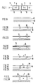
- FIG. 2 The individual steps of the method according to the invention are shown schematically in FIG. 2, progressively from top to bottom. They are designated in the drawing with the letters A to M, which correspond to process steps a) to m) of claim 1. These letters therefore denote the successive process steps, but not or only indirectly the individual material layers.
- a photostructurable film 11 is laminated onto a copper-clad or metallized carrier material 10.
- the carrier 4 consists, for example, of the glass fiber-reinforced plastic known under the name FR4, the photostructurable film 11 consists of a permanent resist, for example a solder resist film with final hardening.
- the photostructurable film 11 is subjected to a photoprocess, which consists in a known manner of exposing the remaining areas and a subsequent development process. Areas 12 corresponding to the position of the outer conductor 7 of the finished signal line 1 or 2 are removed.
- the removed areas 12 are filled with copper by electrodeposition.
- a thin conductive layer 14 is applied to the outer surface of the remaining areas of the film 11 and the outer conductor areas 12 filled with copper by chemical deposition of copper. This conductor layer 14 is connected to the copper layer 10 in an electrically conductive manner via the region 12.
- a photoresist film 15 is applied to the conductive layer 14 and regions 16 which correspond to the position of the inner conductor 6 of the signal lines 1 or 2 are removed from this by a new photoprocess.
- the regions 16 are brought to the strength required for a signal conductor by electrodeposition of copper.
- the remaining areas of the photoresist film are stripped, ie chemically dissolved.
- the conductive layer 14 exposed by stripping the photoresist film 15 is removed by a copper differential etching.
- the lower half of the outer conductor 7 is made and the inner conductor 6 from the other conductive areas, i.e. from the outer conductor 7, galvanically isolated.
- Another photostructurable film 18 is laminated onto the exposed surface. This is indicated in the drawing by a dashed line.
- This film 18 also consists of a permanent resist, e.g. a solder resist in foil form.
- the film 18 is removed in areas 19 which correspond to the upper part of the outer conductor 7 by a further photo process.
- the removed areas 19 are filled with copper by electrodeposition.
- a thin conductive layer 20 is applied to the free surface of the remaining foil 18 and the areas 19 filled with copper by chemical deposition of copper.
Abstract
Description
Die Erfindung betrifft ein Verfahren zum Herstellen einer allseitig geschirmten Signalleitung für Hochfrequenzschaltungen. Derartige allseitig geschirmte Signalleitungen sind z.B. Koaxialleitungen mit rechteckigem Querschnitt oder symmetrische allseitig geschirmte Triplateleitungen, wie sie zum Verbinden von Hoch- und Höchstfrequenzschaltungen, insbesondere in integrierten Mikrowellenschaltungen, verwendet werden.The invention relates to a method for producing a signal line shielded on all sides for high-frequency circuits. Such signal lines shielded on all sides are e.g. Coaxial lines with a rectangular cross-section or symmetrical triplate lines shielded on all sides, as are used for connecting high and ultra-high frequency circuits, in particular in integrated microwave circuits.
Ein bekanntes Verfahren zum Herstellen von geschirmten signalleitungen in Halbleiter-Hochfrequenzschaltungen (Proceedings of Electronic Components Conference, Washington, 1985, Seiten 384 bis 388, 386) weist neben anderen Verfahrensschritten im wesentlichen die Schritte a), b) und c) des Verfahrens nach Anspruch 1 auf. Nach dem Verfahrensschritt c) wird dort eine Prepregfolie unter Druck- und Wärmeeinwirkung auflaminiert. Das danach die Leiterbahnen abdeckende Isoliermaterial wird mechanisch entfernt. Eine solche mechanische Bearbeitung ist aber schwierig durchzuführen und erfordert einen hohen Aufwand.A known method for producing shielded signal lines in semiconductor high-frequency circuits (Proceedings of Electronic Components Conference, Washington, 1985, pages 384 to 388, 386) has, in addition to other method steps, essentially steps a), b) and c) of the method according to claim 1 on. After process step c), a prepreg film is laminated there under the action of pressure and heat. That which then covers the conductor tracks Insulating material is removed mechanically. Such mechanical processing is difficult to carry out and requires a lot of effort.
Der Erfindung liegt die Aufgabe zugrunde, ein einfaches und zuverlässiges Verfahren zum Herstellen von allseitig geschirmten Signalleitungen bei Hoch- und Höchstfrequenzschaltungen zu schaffen, die ein Nebensprechen wirksam verhindern.The invention has for its object to provide a simple and reliable method for producing all-sided shielded signal lines in high and ultra-high frequency circuits that effectively prevent crosstalk.
Diese Aufgabe wird erfinderungsgemäß durch ein Verfahren mit den Merkmalen von Patentanspruch 1 gelöst.According to the invention, this object is achieved by a method having the features of patent claim 1.
Vorteilhafte Weiterbildungen der Erfindung sind aus den Unteransprüchen ersichtlich.Advantageous developments of the invention can be seen from the subclaims.
Ein Ausführungsbeispiel der Erfindung wird im folgenden anhand der Zeichnung erläutert. Es zeigen:
- Fig. 1 erfindungsgemäß hergestellte rechteckige Koaxialleitungen im Querschnitt und
- Fig. 2A bis 2M die erfindungsgemäßen Verfahrenschritte in schematischer Darstellung.
- Fig. 1 rectangular coaxial lines produced according to the invention in cross section and
- 2A to 2M, the method steps according to the invention in a schematic representation.
Zwei erfindungsgemäß hergestellte Signalleitungen 1 und 2 sind Bestandteil einer in der Zeichnung (Fig. 1) nur im Ausschnitt dargestellten, in Halbleitertechnik hergestellten Höchstfrequenzschaltung 3. Die Signalleitungen 1 und 2 sind als Rechteck-Koaxialleitungen ausgeführt, die auf einem gemeinsamen Träger 4 angeordnet sind.Two
Der Träger 4 ist z.B. aus einen glasfaserverstärktem Epoxidharz hergestellt. Die Signalleitungen 1, 2 weisen jeweils einen Innenleiter 6 und einen Außenleiter oder eine äußere Schirmwand 7 auf. Der Innenleiter 6 und der Außenleiter 7 sind aus einem gut leitenden Werkstoff, z.B. auf Kupfer, hergestellt.The
Die inneren Hohlräume 8 der Signalleitungen 1, 2 und die Zwischenräume 9 zwischen den Signalleitungen 1 und 2 und sonstigen Schaltungsbestandteilen sind mit einem Dielekrtrikum aufgefüllt, der aus einem photostrukturierbaren Werkstoff, z.B. aus Epoxid oder Polyimid besteht. Diese mit Dielektrikum aufgefüllten Bereiche werden, wie noch anhand von Fig. 2 zu erläutern sein wird, mit Permanentresist-Folien, z.B. aus einem Lötstoppresist mit Endhärtung - hergestellt.The
Die einzelnen Schritte des erfindungsgemäßen Verfahrens sind in Fig. 2 schematisch dargestellt, und zwar fortschreitend von oben nach unten. Sie sind in der Zeichnung mit den Buchstaben A bis M bezeichnet, die den Verfahrensschritten a) bis m) von Anspruch 1 entsprechen. Diese Buchstaben bezeichnen also die aufeinanderfolgenden Verfahrensschritte, nicht aber oder nur indirekt die einzelnen Werkstoffschichten.The individual steps of the method according to the invention are shown schematically in FIG. 2, progressively from top to bottom. They are designated in the drawing with the letters A to M, which correspond to process steps a) to m) of claim 1. These letters therefore denote the successive process steps, but not or only indirectly the individual material layers.
Auf einen mit Kupfer kaschierten oder metallisierten Trägerwerkstoff 10 wird eine photostrukturierbare Folie 11 auflaminiert. Der Träger 4 besteht z.B. aus dem unter der Bezeichnung FR4 bekannten glasfaserverstärkten Kunststoff, die photostrukturierbare Folie 11 aus einem Permanentresist, z.B. aus einem Lötstoppfolienresist mit Endhärtung.A
Die photostrukturierbare Folie 11 wird einem Photoprozeß unterworfen, de in bekannter Weise aus einem Belichten der zu verbleibenden Bereiche und aus einem nachfolgenden Entwicklungsvorgang besteht. Dabei werden Bereiche 12, die der Lage des Außenleiters 7 der fertigen Signalleitung 1 oder 2 entsprechen, abgetragen.The
Die abgetragenen Bereiche 12 werden durch galvanische Abscheidung mit Kupfer aufgefüllt.The removed
Auf die äußere in der Zeichnung obenliegende, Oberfläche der verbleibenden Bereiche der Folie 11 und der mit Kupfer aufgefüllten Außenleiter-Bereiche 12 wird durch chemisches Abscheiden von Kupfer eine dünne Leitschicht 14 aufgebracht. Diese Leiterschicht 14 ist über die Bereich 12 mit der Kupferschicht 10 elektrisch leitend verbunden.A thin
Auf die Leitschicht 14 wird eine Photoresistfolie 15 aufgebracht und durch einen erneuten Photoprozeß werden aus dieser Bereiche 16 abgetragen, die der Lage des Innenleiters 6 der Signalleitungen 1 oder 2 entsprechen.A
Die Bereiche 16 werden durch galvanisches Abscheiden von Kupfer auf die für einen Signalleiter erforderliche Stärke gebracht.The
Die verbleibenden Bereiche der Photoresistfolie werden abgestrippt, d.h. chemisch aufgelöst.The remaining areas of the photoresist film are stripped, ie chemically dissolved.
Die durch das Abstrippen der Photoresistfolie 15 offengelegte Leitschicht 14 wird durch eine Kupfer-Differenzätzung abgetragen. Damit ist die untere Hälfte der Außenleiter 7 hergestellt und der Innenleiter 6 von den anderen leitenden Bereichen, d.h. von dem Außenleiter 7, galvanisch getrennt.The
Eine weitere photostrukturierbare Folie 18 wird auf die freigelegte Oberfläche auflaminiert. Dies ist in der Zeichnung durch eine gestrichelte linie angedeutet. Auch diese Folie 18 besteht aus einem Permanentresist, z.B. einem Lötstoppresist in Folienform.Another
Die Folie 18 wird in Bereichen 19, die dem oberen Teil des Außenleiters 7 entsprechen, durch einen weiteren Photoprozeß abgetragen.The
Die abgetragenen Bereiche 19 werden durch galvanisches Abscheiden mit Kupfer aufgefüllt.The removed
Auf die freie Oberfläche der verbleibenden Folie 18 und der mit Kupfer aufgefüllten Bereiche 19 wird durch chemisches Abscheiden von Kupfer eine dünne Leitschicht 20 aufgebracht.A thin
Schließlich wird auf diese Leitschicht 20 galvanisch solange Kupfer abgeschieden, bis auch hier die erforderliche Wandstärke des Außenleiters 7 erreicht ist.Finally, copper is electrodeposited onto this
Damit ist das Verfahren abgeschlossen. In einem einzigen Herstellungsprozeß können eine oder mehrere allseitig geschirmte Signalleitungen für Hochfrequenzschaltungen gleichzeitig hergestellt werden. Mechanische Bearbeitungsschritte kommen bei diesem Verfahren nicht vor.This completes the process. In a single manufacturing process, one or more signal lines shielded on all sides for high-frequency circuits can be manufactured simultaneously. Mechanical processing steps do not occur with this method.
Claims (4)
Priority Applications (1)
| Application Number | Priority Date | Filing Date | Title |
|---|---|---|---|
| AT89106223T ATE81733T1 (en) | 1988-04-14 | 1989-04-08 | METHOD OF MAKING AN ALL-ROUND SHIELDED SIGNAL LINE. |
Applications Claiming Priority (2)
| Application Number | Priority Date | Filing Date | Title |
|---|---|---|---|
| DE3812414A DE3812414A1 (en) | 1988-04-14 | 1988-04-14 | METHOD FOR PRODUCING AN ALL-SIDED SHIELDED SIGNAL LINE |
| DE3812414 | 1988-04-14 |
Publications (2)
| Publication Number | Publication Date |
|---|---|
| EP0337331A1 true EP0337331A1 (en) | 1989-10-18 |
| EP0337331B1 EP0337331B1 (en) | 1992-10-21 |
Family
ID=6351965
Family Applications (1)
| Application Number | Title | Priority Date | Filing Date |
|---|---|---|---|
| EP19890106223 Expired - Lifetime EP0337331B1 (en) | 1988-04-14 | 1989-04-08 | Method for producing an allround-shielded transmission line |
Country Status (7)
| Country | Link |
|---|---|
| US (1) | US4909909A (en) |
| EP (1) | EP0337331B1 (en) |
| JP (1) | JPH0215517A (en) |
| AT (1) | ATE81733T1 (en) |
| CA (1) | CA1332120C (en) |
| DE (2) | DE3812414A1 (en) |
| ES (1) | ES2036740T3 (en) |
Cited By (6)
| Publication number | Priority date | Publication date | Assignee | Title |
|---|---|---|---|---|
| WO1992022939A1 (en) * | 1991-06-14 | 1992-12-23 | Telefonaktiebolaget Lm Ericsson | A device with flexible, stripline conductors and a method of manufacturing such a device |
| US5298684A (en) * | 1991-06-14 | 1994-03-29 | Telefonaktiebolaget L M Ericsson | Circuit board having a lateral conductive pattern and shielded regions as well as a method of manufacturing such a board |
| FR2699323A1 (en) * | 1992-12-15 | 1994-06-17 | Asulab Sa | Reed switch with 3D metallic microstructure |
| EP0602538A1 (en) * | 1992-12-15 | 1994-06-22 | Asulab S.A. | Reed switch and manufacturing process for suspended three-dimensional metallic microstructures |
| WO1998006243A1 (en) * | 1996-07-31 | 1998-02-12 | Dyconex Patente | Process for producing connecting conductors |
| CN110112523A (en) * | 2019-05-15 | 2019-08-09 | 中国电子科技集团公司第十三研究所 | Micro coaxle structure, the preparation method of micro coaxle structure and mini-coax line |
Families Citing this family (24)
| Publication number | Priority date | Publication date | Assignee | Title |
|---|---|---|---|---|
| JP3241139B2 (en) * | 1993-02-04 | 2001-12-25 | 三菱電機株式会社 | Film carrier signal transmission line |
| DE4446509A1 (en) * | 1994-12-24 | 1996-06-27 | Sel Alcatel Ag | Method for producing conductor tracks on a substrate having depressions |
| US9054094B2 (en) | 1997-04-08 | 2015-06-09 | X2Y Attenuators, Llc | Energy conditioning circuit arrangement for integrated circuit |
| US7321485B2 (en) | 1997-04-08 | 2008-01-22 | X2Y Attenuators, Llc | Arrangement for energy conditioning |
| US7336468B2 (en) | 1997-04-08 | 2008-02-26 | X2Y Attenuators, Llc | Arrangement for energy conditioning |
| SE522650C2 (en) * | 2000-10-31 | 2004-02-24 | Ericsson Telefon Ab L M | Device on a circuit board and method for manufacturing such a device |
| US6770822B2 (en) * | 2002-02-22 | 2004-08-03 | Bridgewave Communications, Inc. | High frequency device packages and methods |
| EP1609206B1 (en) * | 2003-03-04 | 2010-07-28 | Rohm and Haas Electronic Materials, L.L.C. | Coaxial waveguide microstructures and methods of formation thereof |
| JP2008535207A (en) | 2005-03-01 | 2008-08-28 | エックストゥーワイ アテニュエイターズ,エルエルシー | Regulator with coplanar conductor |
| US7312142B2 (en) * | 2005-04-13 | 2007-12-25 | Mutual Pak Technology Co., Ltd. | Method for making cable with a conductive bump array, and method for connecting the cable to a task object |
| KR101593686B1 (en) | 2007-03-20 | 2016-02-12 | 누보트로닉스, 엘.엘.씨 | Integrated electronic components and methods of formation thereof |
| EP1973189B1 (en) | 2007-03-20 | 2012-12-05 | Nuvotronics, LLC | Coaxial transmission line microstructures and methods of formation thereof |
| US20100307798A1 (en) * | 2009-06-03 | 2010-12-09 | Izadian Jamal S | Unified scalable high speed interconnects technologies |
| US20110123783A1 (en) | 2009-11-23 | 2011-05-26 | David Sherrer | Multilayer build processses and devices thereof |
| US8866300B1 (en) | 2011-06-05 | 2014-10-21 | Nuvotronics, Llc | Devices and methods for solder flow control in three-dimensional microstructures |
| EP2731783A4 (en) | 2011-07-13 | 2016-03-09 | Nuvotronics Llc | Methods of fabricating electronic and mechanical structures |
| US9306254B1 (en) | 2013-03-15 | 2016-04-05 | Nuvotronics, Inc. | Substrate-free mechanical interconnection of electronic sub-systems using a spring configuration |
| US9306255B1 (en) | 2013-03-15 | 2016-04-05 | Nuvotronics, Inc. | Microstructure including microstructural waveguide elements and/or IC chips that are mechanically interconnected to each other |
| US10310009B2 (en) | 2014-01-17 | 2019-06-04 | Nuvotronics, Inc | Wafer scale test interface unit and contactors |
| US10847469B2 (en) | 2016-04-26 | 2020-11-24 | Cubic Corporation | CTE compensation for wafer-level and chip-scale packages and assemblies |
| WO2016094129A1 (en) | 2014-12-03 | 2016-06-16 | Nuvotronics, Inc. | Systems and methods for manufacturing stacked circuits and transmission lines |
| US10319654B1 (en) | 2017-12-01 | 2019-06-11 | Cubic Corporation | Integrated chip scale packages |
| US11350520B2 (en) * | 2019-08-08 | 2022-05-31 | At&S Austria Technologie & Systemtechnik Aktiengesellschaft | Component carrier and method of manufacturing the same |
| US20230053890A1 (en) * | 2021-08-17 | 2023-02-23 | International Business Machines Corporation | Ultrahigh isolation stripline circuit |
Citations (2)
| Publication number | Priority date | Publication date | Assignee | Title |
|---|---|---|---|---|
| DE3006117A1 (en) * | 1980-02-19 | 1981-08-27 | Ruwel-Werke Spezialfabrik für Leiterplatten GmbH, 4170 Geldern | METHOD FOR THE PRODUCTION OF CIRCUITS WITH AT LEAST TWO CIRCUITS |
| US4673904A (en) * | 1984-11-14 | 1987-06-16 | Itt Corporation | Micro-coaxial substrate |
Family Cites Families (1)
| Publication number | Priority date | Publication date | Assignee | Title |
|---|---|---|---|---|
| JPS4959287A (en) * | 1972-10-13 | 1974-06-08 |
-
1988
- 1988-04-14 DE DE3812414A patent/DE3812414A1/en not_active Withdrawn
-
1989
- 1989-04-08 EP EP19890106223 patent/EP0337331B1/en not_active Expired - Lifetime
- 1989-04-08 ES ES198989106223T patent/ES2036740T3/en not_active Expired - Lifetime
- 1989-04-08 AT AT89106223T patent/ATE81733T1/en not_active IP Right Cessation
- 1989-04-08 DE DE8989106223T patent/DE58902480D1/en not_active Expired - Lifetime
- 1989-04-13 CA CA000596584A patent/CA1332120C/en not_active Expired - Fee Related
- 1989-04-14 JP JP1095060A patent/JPH0215517A/en active Pending
- 1989-04-14 US US07/338,269 patent/US4909909A/en not_active Expired - Fee Related
Patent Citations (2)
| Publication number | Priority date | Publication date | Assignee | Title |
|---|---|---|---|---|
| DE3006117A1 (en) * | 1980-02-19 | 1981-08-27 | Ruwel-Werke Spezialfabrik für Leiterplatten GmbH, 4170 Geldern | METHOD FOR THE PRODUCTION OF CIRCUITS WITH AT LEAST TWO CIRCUITS |
| US4673904A (en) * | 1984-11-14 | 1987-06-16 | Itt Corporation | Micro-coaxial substrate |
Cited By (10)
| Publication number | Priority date | Publication date | Assignee | Title |
|---|---|---|---|---|
| WO1992022939A1 (en) * | 1991-06-14 | 1992-12-23 | Telefonaktiebolaget Lm Ericsson | A device with flexible, stripline conductors and a method of manufacturing such a device |
| US5298684A (en) * | 1991-06-14 | 1994-03-29 | Telefonaktiebolaget L M Ericsson | Circuit board having a lateral conductive pattern and shielded regions as well as a method of manufacturing such a board |
| US5317292A (en) * | 1991-06-14 | 1994-05-31 | Telefonaktibolaget L M Ericsson | Device with flexible, stripline conductors and a method of manufacturing such a device |
| US5375322A (en) * | 1991-06-14 | 1994-12-27 | Telefonaktiebolaget L M Ericsson | Method of manufacturing circuit board having lateral conductive pattern |
| FR2699323A1 (en) * | 1992-12-15 | 1994-06-17 | Asulab Sa | Reed switch with 3D metallic microstructure |
| EP0602538A1 (en) * | 1992-12-15 | 1994-06-22 | Asulab S.A. | Reed switch and manufacturing process for suspended three-dimensional metallic microstructures |
| WO1998006243A1 (en) * | 1996-07-31 | 1998-02-12 | Dyconex Patente | Process for producing connecting conductors |
| US6486394B1 (en) | 1996-07-31 | 2002-11-26 | Dyconex Patente Ag | Process for producing connecting conductors |
| CN110112523A (en) * | 2019-05-15 | 2019-08-09 | 中国电子科技集团公司第十三研究所 | Micro coaxle structure, the preparation method of micro coaxle structure and mini-coax line |
| CN110112523B (en) * | 2019-05-15 | 2021-06-15 | 中国电子科技集团公司第十三研究所 | Micro coaxial structure, preparation method of micro coaxial structure and micro coaxial line |
Also Published As
| Publication number | Publication date |
|---|---|
| ATE81733T1 (en) | 1992-11-15 |
| ES2036740T3 (en) | 1993-06-01 |
| US4909909A (en) | 1990-03-20 |
| DE58902480D1 (en) | 1992-11-26 |
| EP0337331B1 (en) | 1992-10-21 |
| DE3812414A1 (en) | 1989-10-26 |
| JPH0215517A (en) | 1990-01-19 |
| CA1332120C (en) | 1994-09-27 |
Similar Documents
| Publication | Publication Date | Title |
|---|---|---|
| EP0337331B1 (en) | Method for producing an allround-shielded transmission line | |
| DE2702844C2 (en) | Method of manufacturing a multilayer printed circuit | |
| EP0175045A2 (en) | Method for the production of flexible printed circuit boards for high bending strain with conductive through-holes | |
| EP0658300B1 (en) | Structured printed circuit boards and films and process for producing them | |
| EP0239158B1 (en) | Circuit board for printed circuits, and method of making such a board | |
| DE2017613B2 (en) | Process for the production of coaxial scarf processing arrangements | |
| DE2144137A1 (en) | Method for producing the holes for the connections between electrical circuit layers lying parallel on top of one another in a multilayer circuit package | |
| EP0700630B1 (en) | Foil printed circuit boards and method of producing the same | |
| CH657004A5 (en) | MULTI-LAYER PCB AND METHOD FOR THE PRODUCTION THEREOF. | |
| AT515447B1 (en) | Method for contacting a component embedded in a printed circuit board and printed circuit board | |
| EP0620702A2 (en) | Core for electrical interconnection substrates and electrical interconnection substrates with core, and method for manufacturing the same | |
| EP0584386A1 (en) | Printed circuit board and method of producing printed circuit boards | |
| DE1764671A1 (en) | Integrated magnetic circuit | |
| AT514564B1 (en) | Method for contacting and rewiring | |
| DE2839215A1 (en) | ARRANGEMENT FOR CONNECTING MICROCIRCUITS | |
| DE102009058764A1 (en) | Method for producing an electronic assembly and electronic assembly | |
| DE19625386A1 (en) | Multilayer, double-sided, flexible or rigid electrical and optical circuit board production avoiding chemicals recovery | |
| DE1765341B1 (en) | METHOD OF MANUFACTURING A MULTI-LAYER PRINTED CIRCUIT | |
| EP0931439B1 (en) | Method for building at least two wiring levels on electrically insulated supports | |
| DE2323542A1 (en) | PRINTED CIRCUIT AND METHOD OF MANUFACTURING IT | |
| DE2247977B2 (en) | Process for making double-sided plated through printed circuit boards | |
| DE1665395B1 (en) | METHOD OF MANUFACTURING PRINTED CIRCUIT BOARDS | |
| DE3840207A1 (en) | Method for producing a printed circuit board having a plurality of conductor track levels, and a corresponding multilayer printed circuit board | |
| CH446463A (en) | Process for the production of electrical components and electrical component produced by the process | |
| DE19705003A1 (en) | Two-layer or multilayer circuit arrangement for SMD technique |
Legal Events
| Date | Code | Title | Description |
|---|---|---|---|
| PUAI | Public reference made under article 153(3) epc to a published international application that has entered the european phase |
Free format text: ORIGINAL CODE: 0009012 |
|
| AK | Designated contracting states |
Kind code of ref document: A1 Designated state(s): AT BE CH DE ES FR GB IT LI NL SE |
|
| 17P | Request for examination filed |
Effective date: 19890925 |
|
| 17Q | First examination report despatched |
Effective date: 19920319 |
|
| GRAA | (expected) grant |
Free format text: ORIGINAL CODE: 0009210 |
|
| AK | Designated contracting states |
Kind code of ref document: B1 Designated state(s): AT BE CH DE ES FR GB IT LI NL SE |
|
| REF | Corresponds to: |
Ref document number: 81733 Country of ref document: AT Date of ref document: 19921115 Kind code of ref document: T |
|
| RAP4 | Party data changed (patent owner data changed or rights of a patent transferred) |
Owner name: ALCATEL N.V. Owner name: ALCATEL SEL AKTIENGESELLSCHAFT |
|
| REF | Corresponds to: |
Ref document number: 58902480 Country of ref document: DE Date of ref document: 19921126 |
|
| GBT | Gb: translation of ep patent filed (gb section 77(6)(a)/1977) | ||
| ITF | It: translation for a ep patent filed |
Owner name: DOTT. ANTONIO SERGI |
|
| ET | Fr: translation filed | ||
| REG | Reference to a national code |
Ref country code: ES Ref legal event code: FG2A Ref document number: 2036740 Country of ref document: ES Kind code of ref document: T3 |
|
| PLBE | No opposition filed within time limit |
Free format text: ORIGINAL CODE: 0009261 |
|
| STAA | Information on the status of an ep patent application or granted ep patent |
Free format text: STATUS: NO OPPOSITION FILED WITHIN TIME LIMIT |
|
| 26N | No opposition filed | ||
| EAL | Se: european patent in force in sweden |
Ref document number: 89106223.4 |
|
| PGFP | Annual fee paid to national office [announced via postgrant information from national office to epo] |
Ref country code: GB Payment date: 19970314 Year of fee payment: 9 |
|
| PGFP | Annual fee paid to national office [announced via postgrant information from national office to epo] |
Ref country code: DE Payment date: 19970320 Year of fee payment: 9 Ref country code: BE Payment date: 19970320 Year of fee payment: 9 |
|
| PGFP | Annual fee paid to national office [announced via postgrant information from national office to epo] |
Ref country code: SE Payment date: 19970324 Year of fee payment: 9 Ref country code: AT Payment date: 19970324 Year of fee payment: 9 |
|
| PGFP | Annual fee paid to national office [announced via postgrant information from national office to epo] |
Ref country code: CH Payment date: 19970326 Year of fee payment: 9 |
|
| PGFP | Annual fee paid to national office [announced via postgrant information from national office to epo] |
Ref country code: NL Payment date: 19970331 Year of fee payment: 9 |
|
| PGFP | Annual fee paid to national office [announced via postgrant information from national office to epo] |
Ref country code: ES Payment date: 19970418 Year of fee payment: 9 |
|
| PGFP | Annual fee paid to national office [announced via postgrant information from national office to epo] |
Ref country code: FR Payment date: 19980313 Year of fee payment: 10 |
|
| PG25 | Lapsed in a contracting state [announced via postgrant information from national office to epo] |
Ref country code: GB Free format text: LAPSE BECAUSE OF NON-PAYMENT OF DUE FEES Effective date: 19980408 Ref country code: AT Free format text: LAPSE BECAUSE OF NON-PAYMENT OF DUE FEES Effective date: 19980408 |
|
| PG25 | Lapsed in a contracting state [announced via postgrant information from national office to epo] |
Ref country code: SE Free format text: LAPSE BECAUSE OF NON-PAYMENT OF DUE FEES Effective date: 19980409 |
|
| PG25 | Lapsed in a contracting state [announced via postgrant information from national office to epo] |
Ref country code: ES Free format text: LAPSE BECAUSE OF NON-PAYMENT OF DUE FEES Effective date: 19980411 |
|
| PG25 | Lapsed in a contracting state [announced via postgrant information from national office to epo] |
Ref country code: LI Free format text: LAPSE BECAUSE OF NON-PAYMENT OF DUE FEES Effective date: 19980430 Ref country code: CH Free format text: LAPSE BECAUSE OF NON-PAYMENT OF DUE FEES Effective date: 19980430 Ref country code: BE Free format text: LAPSE BECAUSE OF NON-PAYMENT OF DUE FEES Effective date: 19980430 |
|
| BERE | Be: lapsed |
Owner name: ALCATEL N.V. Effective date: 19980430 |
|
| PG25 | Lapsed in a contracting state [announced via postgrant information from national office to epo] |
Ref country code: NL Free format text: LAPSE BECAUSE OF NON-PAYMENT OF DUE FEES Effective date: 19981101 |
|
| GBPC | Gb: european patent ceased through non-payment of renewal fee |
Effective date: 19980408 |
|
| REG | Reference to a national code |
Ref country code: CH Ref legal event code: PL |
|
| NLV4 | Nl: lapsed or anulled due to non-payment of the annual fee |
Effective date: 19981101 |
|
| EUG | Se: european patent has lapsed |
Ref document number: 89106223.4 |
|
| PG25 | Lapsed in a contracting state [announced via postgrant information from national office to epo] |
Ref country code: DE Free format text: LAPSE BECAUSE OF NON-PAYMENT OF DUE FEES Effective date: 19990202 |
|
| PG25 | Lapsed in a contracting state [announced via postgrant information from national office to epo] |
Ref country code: FR Free format text: LAPSE BECAUSE OF NON-PAYMENT OF DUE FEES Effective date: 19991231 |
|
| REG | Reference to a national code |
Ref country code: FR Ref legal event code: ST |
|
| REG | Reference to a national code |
Ref country code: ES Ref legal event code: FD2A Effective date: 20000403 |
|
| PG25 | Lapsed in a contracting state [announced via postgrant information from national office to epo] |
Ref country code: IT Free format text: LAPSE BECAUSE OF NON-PAYMENT OF DUE FEES;WARNING: LAPSES OF ITALIAN PATENTS WITH EFFECTIVE DATE BEFORE 2007 MAY HAVE OCCURRED AT ANY TIME BEFORE 2007. THE CORRECT EFFECTIVE DATE MAY BE DIFFERENT FROM THE ONE RECORDED. Effective date: 20050408 |