EP0335607B2 - Video display driver apparatus - Google Patents
Video display driver apparatus Download PDFInfo
- Publication number
- EP0335607B2 EP0335607B2 EP89302933A EP89302933A EP0335607B2 EP 0335607 B2 EP0335607 B2 EP 0335607B2 EP 89302933 A EP89302933 A EP 89302933A EP 89302933 A EP89302933 A EP 89302933A EP 0335607 B2 EP0335607 B2 EP 0335607B2
- Authority
- EP
- European Patent Office
- Prior art keywords
- transistor
- emitter
- signal
- coupled
- output
- Prior art date
- Legal status (The legal status is an assumption and is not a legal conclusion. Google has not performed a legal analysis and makes no representation as to the accuracy of the status listed.)
- Expired - Lifetime
Links
Images
Classifications
-
- H—ELECTRICITY
- H04—ELECTRIC COMMUNICATION TECHNIQUE
- H04N—PICTORIAL COMMUNICATION, e.g. TELEVISION
- H04N5/00—Details of television systems
- H04N5/14—Picture signal circuitry for video frequency region
-
- H—ELECTRICITY
- H03—ELECTRONIC CIRCUITRY
- H03F—AMPLIFIERS
- H03F1/00—Details of amplifiers with only discharge tubes, only semiconductor devices or only unspecified devices as amplifying elements
- H03F1/42—Modifications of amplifiers to extend the bandwidth
- H03F1/48—Modifications of amplifiers to extend the bandwidth of aperiodic amplifiers
-
- H—ELECTRICITY
- H03—ELECTRONIC CIRCUITRY
- H03F—AMPLIFIERS
- H03F3/00—Amplifiers with only discharge tubes or only semiconductor devices as amplifying elements
- H03F3/189—High-frequency amplifiers, e.g. radio frequency amplifiers
- H03F3/19—High-frequency amplifiers, e.g. radio frequency amplifiers with semiconductor devices only
-
- H—ELECTRICITY
- H04—ELECTRIC COMMUNICATION TECHNIQUE
- H04N—PICTORIAL COMMUNICATION, e.g. TELEVISION
- H04N5/00—Details of television systems
- H04N5/14—Picture signal circuitry for video frequency region
- H04N5/148—Video amplifiers
Definitions
- This invention concerns a display driver amolifier and output signal coupling network for providing a high level video output signal to an image display device.
- a video signal processing system comprising an image display device having a signal input electrode with an associated capacitance, a displayer driver amplifier having an output circuit for developing a high level video output signal with a magnitude suitable for driving said image display device and a signal coupling path for conveying said video output signal from said output circuit to said video signal input electrode of said image display device; the coupling path comprising a first emitter follower transistor of a first conductivity type having a base input electrode coupled to said output circuit of said driver amplifier, a collector electrode and an emitter output electrode, for isolating said output circuit of said driver amplifier from said capacitance in the presence of said video signal amplitude transients of one polarity; a second emitter follower transistor of a second conductivity type arranged in cascade with said first transistor and having a base electrode
- a video output display driver amplifier provides a high level video output signal to an image display device such as a kinescope.
- the video output signal is conveyed via an output signal coupling path to a signal input electrode of the kinescope, e.g.. a cathode electrode.
- the kinescope signal input electrode can exhibit a capacitance which is large enough to impair the high frequency response of the video signal developed at the output of the driver amplifier Thus it is desirable to reduce the effect of the kinescope capacitance upon the driver amplifier output signal, thereby preventing degraded video signal high frequency response and degraded image resolution.
- a video signal processing system comprising:
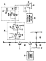
- the sole figure of the drawing illustrates a portion of a television receiver including a video output signal coupling network in accordance with the principles of the present invention.
- a low level video signal from a source 10 is applied to a kinescope driver stage 20 including an input low voltage common emitter amplifier transistor 22 arranged in a cascode video amplifier configuration with an output high voltage common base amplifier transistor 24.
- a high level amplified video signal with a magnitude suitable for driving a signal input cathode electrode 30 of a kinescope 35 is developed in a collector output circuit of transistor 24, including a load resistor 25 coupled to a high operating voltage B + (e.g., +230 volts).
- An amplified video output signal developed across resistor 25 is coupled to cathode electrode 30 via a network 26, a frequency compensated drive level compensation network 27 in accordance with the principles of the present invention, and a kinescope arc current limiting resistor 28, commonly referred to as a "flashover" resistor, operatively associated with network 27.
- the signal gain and the DC bias of driver stage 20 are respectively adjusted by means of a variable resistor 38 and a potentiometer 39 in the emitter circuit of transistor 22.
- Operating voltages for kinescope 35 are provided by a source 36.
- a capacitance C3 represents parasitic kinescope and wiring capacitance associated with kinescope cathode electrode 30.
- the value of this capacitance is approximately 9 picofarads and can result in significant high frequency degradation if it is permitted to influence the video signal developed across resistor 25 in the output circuit of transistor 24.
- Network 26 is arranged to reduce or eliminate such high frequency degradation by decoupling such capacitance from the collector output circuit of transistor 24.
- Coupling network 26 includes an NPN emitter follower transistor 41 with a low impedance emitter output electrode and a PNP emitter follower transistor 42 with a low impedance emitter output electrode arranged in cascade in the output signal path from the collector output circuit of transistor 24 to kinescope 30.
- Parasitic collector-base capacitances C1 and C2. e.g.. 2 picofarads. are respectively associated with transistors 41 and 42 and include stray wiring and layout capacitances.
- Diodes 43 and 44 are coupled across the base-emitter junctions of transistors 41 and 42. respectively. and are poled for forward current conduction in a direction opposite to the forward current conduction direction of the associated base-emitter junction.
- a rapid positive amplitude transition which contains significant high frequency image detail information. is conveyed to kinescope 35 via conductive transistor 41 and conductive diode 44.
- Diode 43 and transistor 42 are reverse biased (nonconductive) at this time.
- the capacitance presented to the collector output of transistor 24 is substantially equal to C1 + C2/ ⁇ 41 + C3/ ⁇ 41 where capacitances C1, C2 and C3 are as discussed above and ⁇ 41 is the forward current gain (Beta) of transistor 41, typically 100 minimum.
- Beta forward current gain
- the value of kinescope capacitance C3 is greatly reduced by the Beta ( ⁇ ) of transistor 41, and the value of relatively small capacitance C2 is reduced further by the Beta of transistor 41.
- Resistor 28 assists to isolate the kinescope capacitance from the output circuit of driver transistor 24, but the effect of such action is much less than that produced by network 26.
- Rapid negative amplitude transitions which also contain significant high frequency image detail information, are conveyed to kinescope 35 via conductive diode 43 and transistor 42.
- Transistor 41 and diode 44 are reverse biased at this time.
- the capacitance presented to the collector output of transistor 24 is substantially equal to C1 + C2 + C3/ ⁇ 42 where ⁇ 42 is the forward current gain of transistor 42, typically 100 minimum.
- ⁇ 42 is the forward current gain of transistor 42, typically 100 minimum.
- a relatively large bypass capacitor 54 shunting a resistor 52 in network 27, as will be discussed subsequently. has a negligible effect upon the value of capacitance given by expressions (1) and (2) above since the value of capacitance presented to the emitter of transistor 42 is dominated by capacitance C3.
- transistors 41 and 42 are not bypassed by capacitors. Such bypassing of one or both of these transistors would defeat the purpose of isolating the output circuit of transistor 24 from capacitances such as kinescope capacitance C3 and capacitor 54 in this example. in the presence of positive or negative signal amplitude transients or both.
- a disolay driver stage including coupling network 26 has been found to exhibit a significant improvement in high frequency response due to decoupling kinescope capacitance C3 from the output circuit of transistor 24. as well as a substantially symmetrical positive and negative transient response.
- expressions (1) and (2) above contain different values of capacitance for positive and negative amplitude transients. The difference is small, however, and transistor 24 can more easily drive a capacitive load when exhibiting increasing current conduction and an associated decreasing collector impedance in response to negative signal amplitude excursions, compared to driving a capacitance when exhibiting decreasing conduction and increasing collector impedance in response to positive amplitude excursions.
- Network 26 can assume configurations other than that shown. For example, when a PNP transistor is employed for driver 24 the positions of transistors 41 and 42 with associated diodes 43 and 44 should be interchanged.
- collector load resistor 25 can be lowered in value because the kinescope does not directly load the collector circuit of transistor 24, i.e., the collector circuit is buffered via follower transistors 41 and 42.
- a lower value of collector load resistance advantageously enhances high frequency response since a smaller resistance value produces less of a lowpass filtering effect together with parasitic collector circuit capacitances.
- Network 27 includes a series coupling resistor 52 and a frequency compensation capacitor 54 arranged in parallel as shown, together with flashover resistor 28.
- a resistor 56 is coupled between an operating voltage (B +) and a point in the signal path to which capacitor 54 is coupled.
- Network 27 compensates for the tendency of an image display device such as kinescope 35 to "bloom", or conduct excessive current, when driven by a large magnitude video signal from a low impedance source such as the emitter output of PNP follower transistor 42.
- resistor 28 and resistor 52 do not develop a significant voltage drop for kinescope current conduction in response to a video signal of low to moderate magnitude.
- resistors 52 and 28 develop a significant voltage drop for kinescope current conduction in response to a large magnitude video signal, e.g.. representative of a bright image. This voltage drop reduces the signal drive to kinescope cathode electrode 30, thereby reducing or eliminating the likelihood that the kinescope will "bloom" under large signal conditions.
- resistors 52 and 28 and capacitor 54 are chosen to yield a desired display drive impedance, particularly at low through middle video signal drive levels which determine image brightness and intensity. so as to maintain kinescope current conduction in accordance with a gamma correction function as is known.
- the values of resistors 52 and 28 can be tailored to provide a desired amount of gamma correction depending on the type of kinescope and its current conduction characteristics.
- Capacitor 54 is a high frequency bypass element to compensate for a high frequency loss associated with a lowpass filtering effect produced by the coaction of kinescope capacitance C3 with resistors 28 and 52.
- the high frequency compensation provided by network 27 begins at approximately 500 KHz, which is well within the DC to 4.2 MHz video signal band according to NTSC standards.
- the amount of high frequency compensation, including high frequency boost, is a function of the values of capacitor 54, resistors 52 and 28, capacitance C3 and the impedance of kinescope cathode 30.
- the impedance of cathode 30 is a function of the current conduction level of cathode 30. In this example, more high frequency compensation is provided at higher cathode current levels.
- Capacitor 54 could be coupled across resistor 28 instead of across resistor 52 as illustrated. However, it is preferred that the non - bypassed resistor be located as close to the kinescope as possible to minimize the damage to circuit boards and associated circuit elements due to kinescope arcing. Placing bypass capacitor 54 across both resistors 52 and 28 would defeat the intended arc current protection since such a capacitor coupling would provide an arc current path circumventing the current limiting effect of resistor 28 in this case.
- Resistor 56 provides a bias for kinescope cathode 30 to assure that the kinescope is blanked during retrace intervals. Resistor 56 also assists capacitor 54 in providing the desired high frequency compensation at various signal drive levels. Specifically, resistor 56 helps to stabilize the effective impedance presented to the network including resistor 52 and capacitor 54. in the presence of kinescope impedance variations associated with changes in the level of kinescope current conduction due to changes in the drive signal level.
Landscapes
- Engineering & Computer Science (AREA)
- Power Engineering (AREA)
- Multimedia (AREA)
- Signal Processing (AREA)
- Picture Signal Circuits (AREA)
- Amplifiers (AREA)
- Control Of Indicators Other Than Cathode Ray Tubes (AREA)
Description
- This invention concerns a display driver amolifier and output signal coupling network for providing a high level video output signal to an image display device.
- There is known from a circuit diagram published by the firm Metz-Werke GmbH & Co KG, Ritterstrasse 5, 90763 Fürth for the television receivers type 7741, 7742 with the chassis 687G a video signal processing system comprising an image display device having a signal input electrode with an associated capacitance, a displayer driver amplifier having an output circuit for developing a high level video output signal with a magnitude suitable for driving said image display device and a signal coupling path for conveying said video output signal from said output circuit to said video signal input electrode of said image display device; the coupling path comprising a first emitter follower transistor of a first conductivity type having a base input electrode coupled to said output circuit of said driver amplifier, a collector electrode and an emitter output electrode, for isolating said output circuit of said driver amplifier from said capacitance in the presence of said video signal amplitude transients of one polarity; a second emitter follower transistor of a second conductivity type arranged in cascade with said first transistor and having a base electrode coupled to said emitter output electrode of said first transistor, a collector electrode and an emitter output electrode coupled to said signal input electrode of said display device; a first unidirectional current conductivity semiconductor device coupled across a base-emitter junction of said first transistor and poled for forward current conduction in a direction opposite to that of said base emitter junction of said first transistor; and a second unidirectional current conductivity semiconductor device coupled across a base-emitter junction of said second transistor and poled for forward current conduction in a direction opposite to that of said base-emitter junction of said second transistor, the second semiconductor device being coupled in parallel with a capacitor.
- In a television receiver a video output display driver amplifier provides a high level video output signal to an image display device such as a kinescope. The video output signal is conveyed via an output signal coupling path to a signal input electrode of the kinescope, e.g.. a cathode electrode. The kinescope signal input electrode can exhibit a capacitance which is large enough to impair the high frequency response of the video signal developed at the output of the driver amplifier Thus it is desirable to reduce the effect of the kinescope capacitance upon the driver amplifier output signal, thereby preventing degraded video signal high frequency response and degraded image resolution.
- According to the present invention. there is provided a video signal processing system comprising:
- an image display device having a signal input electrode with an associated capacitance;
- a display driver amplifier having a signal input for receiving a video signal containing information to be displayed, and having an output circuit for developing a high level video output signal with a magnitude suitable for driving said image display device; and
- a signal coupling path for conveying said video output signal from said output circuit to said signal input electrode of said image display device; wherein for reducing the effect of said capacitance upon said output circuit of said display driver amplifier said signal coupling path comprises:
- a first emitter follower transistor of a first conductivity type having a base input electrode coupled to said output circuit of said driver amplifier, a collector electrode and an emitter output electrode, for isolating said output circuit of said driver amplifier from said capacitance in the presence of video signal amplitude transients of one polarity;
- a second emitter follower transistor of a second conductivity type arranged in cascade with said first transistor and having a base input electrode coupled to said emitter output electrode of said first transistor, a collector electrode and an emitter output electrode coupled to said signal input electrode of said display device, for isolating said output circuit of said driver amplifier from said capacitance in the presence of video signal amplitude transients of another polarity;
- said emitter-follower transistors not being bypassed by capacitors capable of coupling the associated capacitance of said image display device to the output circuit of the display driver amplifier and thereby defeating the isolation provided by said first and second emitter-follower transistors; and
- a first unidirectional current conducting semiconductor device coupled across a base-emitter junction of said first transistor and poled for forward current conduction in a direction opposite to that of said base-emitter junction of said first transistor; and
- a second unidirectional current conducting semiconductor device coupled across a base-emitter junction of said second transistor and poled for forward current conduction in a direction opposite to that of said base-emitter junction of said second transistor.
- The sole figure of the drawing illustrates a portion of a television receiver including a video output signal coupling network in accordance with the principles of the present invention.
- A low level video signal from a
source 10 is applied to akinescope driver stage 20 including an input low voltage commonemitter amplifier transistor 22 arranged in a cascode video amplifier configuration with an output high voltage common base amplifier transistor 24. A high level amplified video signal with a magnitude suitable for driving a signalinput cathode electrode 30 of akinescope 35 is developed in a collector output circuit of transistor 24, including a load resistor 25 coupled to a high operating voltage B + (e.g., +230 volts). An amplified video output signal developed across resistor 25 is coupled tocathode electrode 30 via anetwork 26, a frequency compensated drivelevel compensation network 27 in accordance with the principles of the present invention, and a kinescope arc current limitingresistor 28, commonly referred to as a "flashover" resistor, operatively associated withnetwork 27. The signal gain and the DC bias ofdriver stage 20 are respectively adjusted by means of avariable resistor 38 and apotentiometer 39 in the emitter circuit oftransistor 22. Operating voltages forkinescope 35 are provided by asource 36. - A capacitance C3 represents parasitic kinescope and wiring capacitance associated with
kinescope cathode electrode 30. The value of this capacitance is approximately 9 picofarads and can result in significant high frequency degradation if it is permitted to influence the video signal developed across resistor 25 in the output circuit of transistor 24.Network 26 is arranged to reduce or eliminate such high frequency degradation by decoupling such capacitance from the collector output circuit of transistor 24. -
Coupling network 26 includes an NPNemitter follower transistor 41 with a low impedance emitter output electrode and a PNPemitter follower transistor 42 with a low impedance emitter output electrode arranged in cascade in the output signal path from the collector output circuit of transistor 24 tokinescope 30. Parasitic collector-base capacitances C1 and C2. e.g.. 2 picofarads. are respectively associated withtransistors Diodes transistors - A rapid positive amplitude transition which contains significant high frequency image detail information. is conveyed to
kinescope 35 viaconductive transistor 41 andconductive diode 44.Diode 43 andtransistor 42 are reverse biased (nonconductive) at this time. - In the case of a rapid positive-going video signal amplitude transition at the collector output of transistor 24. the capacitance presented to the collector output of transistor 24 is substantially equal to

transistor 41, typically 100 minimum. Thus at the collector of driver transistor 24 the value of kinescope capacitance C3 is greatly reduced by the Beta (β) oftransistor 41, and the value of relatively small capacitance C2 is reduced further by the Beta oftransistor 41.Resistor 28 assists to isolate the kinescope capacitance from the output circuit of driver transistor 24, but the effect of such action is much less than that produced bynetwork 26. - Rapid negative amplitude transitions, which also contain significant high frequency image detail information, are conveyed to
kinescope 35 viaconductive diode 43 andtransistor 42.Transistor 41 anddiode 44 are reverse biased at this time. For rapid negative-going video signal amplitude transitions at the collector output of transistor 24. the capacitance presented to the collector output of transistor 24 is substantially equal to
transistor 42, typically 100 minimum. Thus the relatively large value of kinescope capacitance C3 is greatly reduced by the Beta oftransistor 42 at the collector of driver transistor 24. - A relatively
large bypass capacitor 54 shunting aresistor 52 innetwork 27, as will be discussed subsequently. has a negligible effect upon the value of capacitance given by expressions (1) and (2) above since the value of capacitance presented to the emitter oftransistor 42 is dominated by capacitance C3. - Note that the base - emitter junctions of
transistors capacitor 54 in this example. in the presence of positive or negative signal amplitude transients or both. - A disolay driver stage including
coupling network 26 has been found to exhibit a significant improvement in high frequency response due to decoupling kinescope capacitance C3 from the output circuit of transistor 24. as well as a substantially symmetrical positive and negative transient response. In the latter regard it is noted that expressions (1) and (2) above contain different values of capacitance for positive and negative amplitude transients. The difference is small, however, and transistor 24 can more easily drive a capacitive load when exhibiting increasing current conduction and an associated decreasing collector impedance in response to negative signal amplitude excursions, compared to driving a capacitance when exhibiting decreasing conduction and increasing collector impedance in response to positive amplitude excursions. -
Network 26 can assume configurations other than that shown. For example, when a PNP transistor is employed for driver 24 the positions oftransistors diodes - With the disclosed arrangement the value of collector load resistor 25 can be lowered in value because the kinescope does not directly load the collector circuit of transistor 24, i.e., the collector circuit is buffered via
follower transistors -
Network 27 includes aseries coupling resistor 52 and afrequency compensation capacitor 54 arranged in parallel as shown, together withflashover resistor 28. Aresistor 56 is coupled between an operating voltage (B +) and a point in the signal path to whichcapacitor 54 is coupled. -
Network 27 compensates for the tendency of an image display device such askinescope 35 to "bloom", or conduct excessive current, when driven by a large magnitude video signal from a low impedance source such as the emitter output ofPNP follower transistor 42. To thisend resistor 28 andresistor 52 do not develop a significant voltage drop for kinescope current conduction in response to a video signal of low to moderate magnitude. However,resistors kinescope cathode electrode 30, thereby reducing or eliminating the likelihood that the kinescope will "bloom" under large signal conditions. The values ofresistors capacitor 54 are chosen to yield a desired display drive impedance, particularly at low through middle video signal drive levels which determine image brightness and intensity. so as to maintain kinescope current conduction in accordance with a gamma correction function as is known. The values ofresistors -
Capacitor 54 is a high frequency bypass element to compensate for a high frequency loss associated with a lowpass filtering effect produced by the coaction of kinescope capacitance C3 withresistors network 27 begins at approximately 500 KHz, which is well within the DC to 4.2 MHz video signal band according to NTSC standards. The amount of high frequency compensation, including high frequency boost, is a function of the values ofcapacitor 54,resistors kinescope cathode 30. The impedance ofcathode 30 is a function of the current conduction level ofcathode 30. In this example, more high frequency compensation is provided at higher cathode current levels. -
Capacitor 54 could be coupled acrossresistor 28 instead of acrossresistor 52 as illustrated. However, it is preferred that the non - bypassed resistor be located as close to the kinescope as possible to minimize the damage to circuit boards and associated circuit elements due to kinescope arcing. Placingbypass capacitor 54 across bothresistors resistor 28 in this case. -
Resistor 56 provides a bias forkinescope cathode 30 to assure that the kinescope is blanked during retrace intervals.Resistor 56 also assistscapacitor 54 in providing the desired high frequency compensation at various signal drive levels. Specifically,resistor 56 helps to stabilize the effective impedance presented to thenetwork including resistor 52 andcapacitor 54. in the presence of kinescope impedance variations associated with changes in the level of kinescope current conduction due to changes in the drive signal level.
Claims (5)
- A video signal processing system comprising:an image display device (35) having a signal input electrode with an associated capacitance;a display driver amplifier (20) having a signal input for receiving a video signal containing information to be displayed, and having an output circuit for developing a high level video output signal with a magnitude suitable for driving said image display device; anda signal coupling path (26,27) for conveying said video output signal from said output circuit to said signal input electrode (30) of said image display device (35); wherein for reducing the effect of said capacitance upon said output circuit of said display driver amplifier said signal coupling path comprises:a first emitter follower transistor (41) of a first conductivity type having a base input electrode coupled to said output circuit of said driver amplifier (20), a collector electrode and an emitter output electrode, for isolating said output circuit of said driver amplifier from said capacitance in the presence of video signal amplitude transients of one polarity;a second emitter follower transistor (42) of a second conductivity type arranged in cascade with said first transistor (41) and having a base input electrode coupled to said emitter output electrode of said first transistor, a collector electrode and an emitter output electrode coupled to said signal input electrode of said display device, for isolating said output circuit of said driver amplifier (20) from said capacitance in the presence of video signal amplitude transients of another polarity;said emitter-follower transistors not being bypassed by capacitors capable of coupling the associated capacitance of said image display device to the output circuit of the display driver amplifier and thereby defeating the isolation provided by said first and second emitter-follower transistors; anda first unidirectional current conducting semiconductor device (43) coupled across a base-emitter junction of said first transistor and poled for forward current conduction in a direction opposite to that of said base-emitter junction of said first transistor; anda second unidirectional current conducting semiconductor device (44) coupled across a base-emitter junction of said second transistor and poled for forward current conduction in a direction opposite to that of said base-emitter junction of said second transistor.
- A system according to Claim 1, characterized in that
said display driver amplifier (20) includes a transistor (24) of the same conductivity type as said first transistor. - A system according to Claim 1 or 2, characterized in that
said first (41) and second (42) transistors are NPN and PNP devices, respectively. - A system according to any one of the preceding claims characterized in that said signal coupling path includesfirst (52) and second (28) resistors coupled in series in the order named from said emitter output of said second transistor to said signal input electrode of said image display device; anda capacitor (54) coupled across said first resistor.
- A system according to Claim 4 further characterized by
a third resistor (56) coupled from a voltage source to a point between said first and second resistors.
Applications Claiming Priority (2)
| Application Number | Priority Date | Filing Date | Title |
|---|---|---|---|
| US07/174,057 US4860107A (en) | 1988-03-28 | 1988-03-28 | Video display driver apparatus |
| US174057 | 1988-03-28 |
Publications (3)
| Publication Number | Publication Date |
|---|---|
| EP0335607A1 EP0335607A1 (en) | 1989-10-04 |
| EP0335607B1 EP0335607B1 (en) | 1993-05-19 |
| EP0335607B2 true EP0335607B2 (en) | 1996-10-16 |
Family
ID=22634628
Family Applications (1)
| Application Number | Title | Priority Date | Filing Date |
|---|---|---|---|
| EP89302933A Expired - Lifetime EP0335607B2 (en) | 1988-03-28 | 1989-03-23 | Video display driver apparatus |
Country Status (10)
| Country | Link |
|---|---|
| US (1) | US4860107A (en) |
| EP (1) | EP0335607B2 (en) |
| JP (1) | JPH0759045B2 (en) |
| KR (1) | KR0136886B1 (en) |
| CN (1) | CN1018134B (en) |
| CA (1) | CA1292557C (en) |
| DE (1) | DE68906584T3 (en) |
| ES (1) | ES2040462T5 (en) |
| FI (1) | FI90611C (en) |
| MY (1) | MY103840A (en) |
Families Citing this family (6)
| Publication number | Priority date | Publication date | Assignee | Title |
|---|---|---|---|---|
| TW280037B (en) * | 1994-04-22 | 1996-07-01 | Handotai Energy Kenkyusho Kk | Drive circuit of active matrix type display device and manufacturing method |
| CA2145901C (en) * | 1994-04-28 | 2000-02-22 | Anton Werner Keller | Kinescope driver apparatus with gamma correction |
| US5525931A (en) * | 1995-04-25 | 1996-06-11 | National Semiconductor Corporation | High-speed video amplifier |
| US5680173A (en) * | 1995-06-23 | 1997-10-21 | Thomson Consumer Electronics, Inc. | Kinescope driver apparatus |
| CN1053077C (en) * | 1995-12-06 | 2000-05-31 | 明碁电脑股份有限公司 | Color Cathode Ray Tube Moiré Phenomenon Improvement Circuit |
| US5969762A (en) * | 1997-02-26 | 1999-10-19 | Thomson Consumer Electronics, Inc. | Video signal driver including a cascode transistor |
Family Cites Families (4)
| Publication number | Priority date | Publication date | Assignee | Title |
|---|---|---|---|---|
| DE2960094D1 (en) * | 1978-03-16 | 1981-03-19 | Videocolor Sa | Apparatus for generating the cut-off voltage of a cathode-ray-tube and colour television receiver embodying such an apparatus |
| DE2840822C3 (en) * | 1978-09-20 | 1981-06-04 | Robert Bosch Gmbh, 7000 Stuttgart | Circuit arrangement for amplifying video signals |
| US4589032A (en) * | 1984-04-05 | 1986-05-13 | Rockwell International Corporation | Ultra low power video amplifier |
| US4631595A (en) * | 1985-07-25 | 1986-12-23 | Rca Corporation | Feedback display driver stage |
-
1988
- 1988-03-28 US US07/174,057 patent/US4860107A/en not_active Expired - Lifetime
-
1989
- 1989-02-23 CA CA000591894A patent/CA1292557C/en not_active Expired - Lifetime
- 1989-03-08 MY MYPI89000277A patent/MY103840A/en unknown
- 1989-03-21 FI FI891337A patent/FI90611C/en not_active IP Right Cessation
- 1989-03-23 EP EP89302933A patent/EP0335607B2/en not_active Expired - Lifetime
- 1989-03-23 DE DE68906584T patent/DE68906584T3/en not_active Expired - Fee Related
- 1989-03-23 ES ES89302933T patent/ES2040462T5/en not_active Expired - Lifetime
- 1989-03-23 CN CN89101768A patent/CN1018134B/en not_active Expired
- 1989-03-27 KR KR1019890003815A patent/KR0136886B1/en not_active Expired - Fee Related
- 1989-03-27 JP JP1072066A patent/JPH0759045B2/en not_active Expired - Fee Related
Also Published As
| Publication number | Publication date |
|---|---|
| MY103840A (en) | 1993-09-30 |
| US4860107A (en) | 1989-08-22 |
| CN1036678A (en) | 1989-10-25 |
| DE68906584T3 (en) | 1997-04-17 |
| JPH0759045B2 (en) | 1995-06-21 |
| DE68906584T2 (en) | 1994-01-05 |
| EP0335607A1 (en) | 1989-10-04 |
| KR890015575A (en) | 1989-10-30 |
| ES2040462T5 (en) | 1996-12-16 |
| FI891337A7 (en) | 1989-09-29 |
| KR0136886B1 (en) | 1998-04-28 |
| DE68906584D1 (en) | 1993-06-24 |
| CA1292557C (en) | 1991-11-26 |
| EP0335607B1 (en) | 1993-05-19 |
| FI891337A0 (en) | 1989-03-21 |
| CN1018134B (en) | 1992-09-02 |
| ES2040462T3 (en) | 1993-10-16 |
| FI90611C (en) | 1994-02-25 |
| FI90611B (en) | 1993-11-15 |
| JPH0211067A (en) | 1990-01-16 |
Similar Documents
| Publication | Publication Date | Title |
|---|---|---|
| GB2149610A (en) | Video signal dc restoration circuit | |
| EP0335604B1 (en) | Video display driver coupling circuit | |
| US4860107A (en) | Video display driver apparatus | |
| GB2149269A (en) | Driver amplifier for an image display device | |
| US4727336A (en) | Wide band low power loss video amplifier | |
| CA1078504A (en) | Video amplifier including an a-c coupled voltage follower output stage | |
| US4642696A (en) | Kinescope driver with kinescope current sensing circuit | |
| US4682233A (en) | Video output signal clamping circuit | |
| US4547799A (en) | Feedback kinescope driver | |
| EP0196695A1 (en) | Picture display device | |
| US4631595A (en) | Feedback display driver stage | |
| US4591912A (en) | Peaking circuit for video driver stage | |
| US3969579A (en) | Contrast, brightness and peaking control circuit | |
| KR930004638B1 (en) | Video signal processing device with high frequency compensation | |
| CN1286866A (en) | Display driver apparatus | |
| KR820000914B1 (en) | Combined blanking level and kinescope bias clamp for a television signal processing system | |
| KR890007188Y1 (en) | Noise pulse cancellation circuit of video signal | |
| JPH0870395A (en) | Linearity correction circuit | |
| NL8602822A (en) | Horizontal aperture correction circuit for TV and still pictures - forms active low pass filter from transistor with feedback resistor and capacitor |
Legal Events
| Date | Code | Title | Description |
|---|---|---|---|
| PUAI | Public reference made under article 153(3) epc to a published international application that has entered the european phase |
Free format text: ORIGINAL CODE: 0009012 |
|
| AK | Designated contracting states |
Kind code of ref document: A1 Designated state(s): DE ES FR GB IT SE |
|
| 17P | Request for examination filed |
Effective date: 19900308 |
|
| 17Q | First examination report despatched |
Effective date: 19920211 |
|
| GRAA | (expected) grant |
Free format text: ORIGINAL CODE: 0009210 |
|
| AK | Designated contracting states |
Kind code of ref document: B1 Designated state(s): DE ES FR GB IT SE |
|
| PG25 | Lapsed in a contracting state [announced via postgrant information from national office to epo] |
Ref country code: SE Effective date: 19930519 |
|
| ITF | It: translation for a ep patent filed | ||
| REF | Corresponds to: |
Ref document number: 68906584 Country of ref document: DE Date of ref document: 19930624 |
|
| ET | Fr: translation filed | ||
| REG | Reference to a national code |
Ref country code: ES Ref legal event code: FG2A Ref document number: 2040462 Country of ref document: ES Kind code of ref document: T5 |
|
| PLBI | Opposition filed |
Free format text: ORIGINAL CODE: 0009260 |
|
| 26 | Opposition filed |
Opponent name: INTERESSENGEMEINSCHAFT FUER RUNDFUNKSCHUTZRECHTE E Effective date: 19940205 |
|
| PLAB | Opposition data, opponent's data or that of the opponent's representative modified |
Free format text: ORIGINAL CODE: 0009299OPPO |
|
| R26 | Opposition filed (corrected) |
Opponent name: INTERESSENGEMEINSCHAFT FUER RUNDFUNKSCHUTZRECHTE E Effective date: 19940205 |
|
| PLAW | Interlocutory decision in opposition |
Free format text: ORIGINAL CODE: EPIDOS IDOP |
|
| PLAW | Interlocutory decision in opposition |
Free format text: ORIGINAL CODE: EPIDOS IDOP |
|
| PUAH | Patent maintained in amended form |
Free format text: ORIGINAL CODE: 0009272 |
|
| STAA | Information on the status of an ep patent application or granted ep patent |
Free format text: STATUS: PATENT MAINTAINED AS AMENDED |
|
| 27A | Patent maintained in amended form |
Effective date: 19961016 |
|
| AK | Designated contracting states |
Kind code of ref document: B2 Designated state(s): DE ES FR GB IT SE |
|
| ET3 | Fr: translation filed ** decision concerning opposition | ||
| REG | Reference to a national code |
Ref country code: ES Ref legal event code: DC2A Kind code of ref document: T5 Effective date: 19961106 |
|
| ITF | It: translation for a ep patent filed | ||
| REG | Reference to a national code |
Ref country code: GB Ref legal event code: IF02 |
|
| REG | Reference to a national code |
Ref country code: FR Ref legal event code: D6 |
|
| REG | Reference to a national code |
Ref country code: GB Ref legal event code: 746 Effective date: 20030103 |
|
| PGFP | Annual fee paid to national office [announced via postgrant information from national office to epo] |
Ref country code: ES Payment date: 20060306 Year of fee payment: 18 |
|
| PGFP | Annual fee paid to national office [announced via postgrant information from national office to epo] |
Ref country code: DE Payment date: 20060322 Year of fee payment: 18 |
|
| PGFP | Annual fee paid to national office [announced via postgrant information from national office to epo] |
Ref country code: FR Payment date: 20060330 Year of fee payment: 18 |
|
| PGFP | Annual fee paid to national office [announced via postgrant information from national office to epo] |
Ref country code: IT Payment date: 20060331 Year of fee payment: 18 |
|
| PGFP | Annual fee paid to national office [announced via postgrant information from national office to epo] |
Ref country code: GB Payment date: 20070202 Year of fee payment: 19 |
|
| REG | Reference to a national code |
Ref country code: FR Ref legal event code: ST Effective date: 20071130 |
|
| PG25 | Lapsed in a contracting state [announced via postgrant information from national office to epo] |
Ref country code: DE Free format text: LAPSE BECAUSE OF NON-PAYMENT OF DUE FEES Effective date: 20071002 |
|
| REG | Reference to a national code |
Ref country code: ES Ref legal event code: FD2A Effective date: 20070324 |
|
| PG25 | Lapsed in a contracting state [announced via postgrant information from national office to epo] |
Ref country code: FR Free format text: LAPSE BECAUSE OF NON-PAYMENT OF DUE FEES Effective date: 20070402 Ref country code: ES Free format text: LAPSE BECAUSE OF NON-PAYMENT OF DUE FEES Effective date: 20070324 |
|
| GBPC | Gb: european patent ceased through non-payment of renewal fee |
Effective date: 20080323 |
|
| PG25 | Lapsed in a contracting state [announced via postgrant information from national office to epo] |
Ref country code: GB Free format text: LAPSE BECAUSE OF NON-PAYMENT OF DUE FEES Effective date: 20080323 |
|
| PG25 | Lapsed in a contracting state [announced via postgrant information from national office to epo] |
Ref country code: IT Free format text: LAPSE BECAUSE OF NON-PAYMENT OF DUE FEES Effective date: 20070323 |