EP0332436A2 - Series resonant power converter and method of controlling the same - Google Patents
Series resonant power converter and method of controlling the same Download PDFInfo
- Publication number
- EP0332436A2 EP0332436A2 EP89302335A EP89302335A EP0332436A2 EP 0332436 A2 EP0332436 A2 EP 0332436A2 EP 89302335 A EP89302335 A EP 89302335A EP 89302335 A EP89302335 A EP 89302335A EP 0332436 A2 EP0332436 A2 EP 0332436A2
- Authority
- EP
- European Patent Office
- Prior art keywords
- resonant
- circuit
- switch means
- voltage
- detecting
- Prior art date
- Legal status (The legal status is an assumption and is not a legal conclusion. Google has not performed a legal analysis and makes no representation as to the accuracy of the status listed.)
- Granted
Links
Images


Classifications
-
- H—ELECTRICITY
- H02—GENERATION; CONVERSION OR DISTRIBUTION OF ELECTRIC POWER
- H02M—APPARATUS FOR CONVERSION BETWEEN AC AND AC, BETWEEN AC AND DC, OR BETWEEN DC AND DC, AND FOR USE WITH MAINS OR SIMILAR POWER SUPPLY SYSTEMS; CONVERSION OF DC OR AC INPUT POWER INTO SURGE OUTPUT POWER; CONTROL OR REGULATION THEREOF
- H02M3/00—Conversion of dc power input into dc power output
- H02M3/22—Conversion of dc power input into dc power output with intermediate conversion into ac
- H02M3/24—Conversion of dc power input into dc power output with intermediate conversion into ac by static converters
- H02M3/28—Conversion of dc power input into dc power output with intermediate conversion into ac by static converters using discharge tubes with control electrode or semiconductor devices with control electrode to produce the intermediate ac
- H02M3/325—Conversion of dc power input into dc power output with intermediate conversion into ac by static converters using discharge tubes with control electrode or semiconductor devices with control electrode to produce the intermediate ac using devices of a triode or a transistor type requiring continuous application of a control signal
- H02M3/335—Conversion of dc power input into dc power output with intermediate conversion into ac by static converters using discharge tubes with control electrode or semiconductor devices with control electrode to produce the intermediate ac using devices of a triode or a transistor type requiring continuous application of a control signal using semiconductor devices only
- H02M3/337—Conversion of dc power input into dc power output with intermediate conversion into ac by static converters using discharge tubes with control electrode or semiconductor devices with control electrode to produce the intermediate ac using devices of a triode or a transistor type requiring continuous application of a control signal using semiconductor devices only in push-pull configuration
- H02M3/3376—Conversion of dc power input into dc power output with intermediate conversion into ac by static converters using discharge tubes with control electrode or semiconductor devices with control electrode to produce the intermediate ac using devices of a triode or a transistor type requiring continuous application of a control signal using semiconductor devices only in push-pull configuration with automatic control of output voltage or current
-
- Y—GENERAL TAGGING OF NEW TECHNOLOGICAL DEVELOPMENTS; GENERAL TAGGING OF CROSS-SECTIONAL TECHNOLOGIES SPANNING OVER SEVERAL SECTIONS OF THE IPC; TECHNICAL SUBJECTS COVERED BY FORMER USPC CROSS-REFERENCE ART COLLECTIONS [XRACs] AND DIGESTS
- Y02—TECHNOLOGIES OR APPLICATIONS FOR MITIGATION OR ADAPTATION AGAINST CLIMATE CHANGE
- Y02B—CLIMATE CHANGE MITIGATION TECHNOLOGIES RELATED TO BUILDINGS, e.g. HOUSING, HOUSE APPLIANCES OR RELATED END-USER APPLICATIONS
- Y02B70/00—Technologies for an efficient end-user side electric power management and consumption
- Y02B70/10—Technologies improving the efficiency by using switched-mode power supplies [SMPS], i.e. efficient power electronics conversion e.g. power factor correction or reduction of losses in power supplies or efficient standby modes
Definitions
- the present invention relates to a series resonant power converter for producing a desired DC voltage for a load, and a method of controlling such series resonant converter.
- a value of a resonant current of a series resonant converter depends on values of an inductance of a resonant reactor, a capacitance of a resonant capacitor, a DC input voltage and a DC output voltage. Accordingly, many researches have been made on a relationship between these values and the resonant current. As the result of these researches, it has been found that in order to control the output voltage of the series resonant power converter at a constant voltage, without controlling the value of the output current, it is necessary to adjust the value of the output current (average value of the resonant current) by control of OFF-periods of a main switch means (that is, frequency control).
- a series resonant converter as shown in Fig. 3, in which a tank circuit consisting of parallel resonant circuits having an infinite impedance at its resonant frequency is inserted in the series resonant circuit loop, whereby an impedance of the resonant circuit is increased under a light load condition and thus the load dependent characteristic of the operating frequency is minimized.
- the series resonant converter shown in Fig. 3 includes a first circuit 13 having switch means 11 and 12, such as bipolar transistors, connected together in series in forward direction, a second circuit 16 having diodes 14 and 15 connected together in series in forward direction, a third circuit 19 having resonant capacitors 17 and 18 connected together in series and a DC power source 21 connected across both ends of these circuits.
- the switch means 11 and 12 are arranged in forward direction relatively to the DC power source 21 but the diodes 14 and 15 are arranged to have opposite polarities.
- a juncture of the diodes 14 and 15 and a juncture of the resonant capacitors 17 and 18 are connected with each other, and a fourth circuit 24 is connected between the juncture 22 of the resonant capacitors 17 and 18 and a juncture 23 of the switch means 11 and 12.
- the fourth circuit 24 includes a rectifying circuit 25, a resonant inductor 26 and a tank circuit 27, which are connected in series with each other, and said tank circuit 27 consists of a parallel circuit including a resonant inductor 28 and a resonant capacitor 29.
- the rectifying circuit 25 consists of a bridge circuit including diodes 31 - 34. An output capacitor 35 is connected across output terminals of said bridge circuit and a load 36 is connected in parallel with said output capacitor 35.
- the resonant capacitor 17 has been charged up to a voltage of the DC power source 21 and the resonant capacitor 18 has been discharged to a zero voltage.
- the semiconductor switch 11 is turned ON, a current i1 flows from the DC power source 21 ⁇ the semiconductor switch 11 ⁇ the diode 31 of the rectifying circuit 25 ⁇ the load 36 (capacitor 35) ⁇ the diode 33 of the rectifying circuit 25 ⁇ the resonant inductor 26 ⁇ the tank circuit 27 to the resonant capacitor 18.
- a discharging current i2 flows from the switch means 11 ⁇ the diode 31 of the rectifying circuit 25 ⁇ the load 36 (capacitor 35) ⁇ the diode 33 of the rectifying circuit 25 ⁇ the resonant inductor 26 ⁇ the tank circuit 27 to the resonant capacitor 17.
- This current is a resonant current which discharges the resonant capacitor 17 and charges the resonant capacitor 18.
- the capacitance C p of the capacitor 29 is set at a value higher than the capacitance C s of the resonant capacitor 17 (or the resonant capacitor 18), so that the voltage of the resonant capacitor 17 becomes zero and the voltage of the resonant capacitor 18 becomes equal to the power source voltage V i , after the lapse of about ⁇ 2 L s ⁇ C s ⁇ - cos ⁇ 1 (V o /(V i -V o )) ⁇ sec, where V o is a voltage (output voltage) of the output capacitor 35, L s is an inductance of the resonant inductor 26 and V i is a voltage of the DC power source 21.
- the diode 14 becomes conductive and the current which has passed through the resonant inductor 26, flows as the current i2 from the resonant inductor 26 ⁇ the tank circuit 27 ⁇ the diode 14 ⁇ the switch means 11 ⁇ the rectifying circuit 25 ⁇ the load 36 (capacitor 35) ⁇ the rectifying circuit 25. This current i2 is consumed by the load 36, until it becomes zero.
- f0 is set at a value substantially lower than f1 and the impedance of the tank circuit 27 is increased at around f1, so that the minimum operating frequency of the converter is clamped at f0. That is, the operating frequency of the converter should be controlled to be increased so that it becomes higher than an audible range, thereby preventing noise scattering.
- the operating frequency of the converter should be controlled to be decreased.
- By using such additional parallel resonant tank circuit it is possible to operate the converter with good result even under light load condition, without the need of lowering the operating frequency of the converter to the audible frequency range.
- in order to hold the output voltage or the output current at constant it is usual to detect a variation thereof thereby automatically controlling the operating frequency.
- the capacitance of the resonant capacitor 29 in the parallel resonant tank circuit 27 must have a high value, at least four to five times as high as that of the resonant capacitor 17 or 18. Furthermore, the energy handled by the parallel resonant circuit 27 must have a value corresponding to Q times as high as the energy transmitted to the output side, where Q is the Q factor of the parallel resonant tank circuit. Accordingly, the resonant inductor used must be of large size, with the result that the power dissipation is increased. Furthermore, it is necessary to separately provide a resonant capacitor having a large capacitance, for the tank circuit 27.
- a series resonant circuit which comprises a first circuit including a first switch means and a second switch means connected in series with each other in a forward direction; a second circuit including a first diode and a second diode connected in series with each other in a forward direction; a third circuit including a first resonant capacitor and a second resonant capacitor connected in series with each other; a DC power source connected across both ends of said first, second and third circuits; a first resonant inductor connected in a path of a main current flowing through said first switch means or said second switch means, said first resonant inductor being connected, at its one end, to a juncture of said first switch means with said second switch means and, at its other end, to a juncture of said first diode and said second diode and a juncture of said first resonant capacitor with said second resonant capacitor; and a second resonant inductor connected,
- the resonant capacitor is commonly used in the series resonant circuit and the parallel resonant circuit and the capacitance of the resonant capacitor can be considerably decreased, as compared with the one used in the conventional tank circuit, so that the energy handled by the resonant capacitor can be decreased. Accordingly, the size of the resonant inductor can be decreased and the power loss can be minimized.
- a method of controlling a series resonant converter including a first resonant circuit consisting of one of a first main switch means and a second main switch means which is in ON-state and a main transformer, and a second resonant circuit, in which ON-OFF operation of the first or second main switch means is controlled by an output power control signal, to produce a predetermined DC output power
- said method comprising: a step of causing said first or second main switch means to be turned ON by a voltage state detecting signal, thereby avoiding temporary interruption of wave form and sustaining oscillating operation, when a value conversed to a primary side from a value of a voltage applied across said first or second main switch means minus an output voltage drops below a reference voltage (K), in the case where the above-mentioned output control signal has not been generated at a transient time owing to variation of the load condition, variation of input voltage or the like.
- K reference voltage
- the series resonant converter as described above includes means for detecting and computing a voltage applied across the main switch means when it is in OFF-state, and a control circuit which is arranged to cause the main switch means to be driven at the time when the voltage computed as above becomes a minimum voltage required to sustain the oscillation of the series resonant converter.
- This minimum voltage can be computed by a detecting circuit for detecting the input voltage, a detecting circuit for detecting a voltage of the second resonant circuit and a detecting circuit for detecting a DC output voltage conversed to a primary side of the main transformer.
- the temporary interruption of the operating wave form which may happen at a transient time responsive to starting of operation, variation of the load condition, variation of input voltage can be avoided, and the stable control of the converter can be obtained.
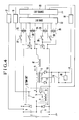
- Fig. 1 indicate main switch means; 13 indicates a first circuit; 14 and 15 indicate diodes; 16 indicates a second circuit; 17 and 18 indicate resonant capacitors; 19 indicates a third circuit; 21 indicates a DC power source; 26 and 28 indicate resonant inductors; and 40 indicates a transformer.
- the resonant inductor 28 is connected, at its one end, to a point A, which forms a juncture between the diodes 14 and 15 of the second circuit 16 and a juncture between the resonant capacitors 17 and 18 of the third circuit 19 and, at its other end, to a neutral voltage point B of the DC power source 21.
- the resonant capacitors 17 and 18 produces a parallel resonance with the resonant inductor 18, and these resonant capacitor produce series resonance with the resonant inductor 26, respectively.
- the main current flowing through the first circuit 13 flows through the third circuit 19.
- the charging current serves to charge the resonant capacitor 18 up to substantially the source voltage, and after the resonant capacitor 17 has discharged to substantially zero voltage, the diode 14 of the second circuit 16 becomes conductive and the energy accumulated at the resonant inductor 16 is transferred through the diode 14 ⁇ switch means 11 ⁇ transformer 40 to the output side. After the OFF period of the switch means 11 and 12, the switch means 12 is turned ON. The ON operation of the switch means 12 is same as that of the switch means 11 and so the detailed description thereof is omitted.
- the diodes 14 and 15 are connected in parallel with the resonant capacitors 17 and 18 of the third circuit 19, respectively, and consequently they are not adversely affected by the recovery of the diodes 14 and 15.
- the switch means 11 or 12 is turned ON under a state of voltage at the juncture A where a voltage across the switch means 11 or 12 is of a lower voltage (a voltage having small amplitude corresponding to the voltage of the DC power source 21A or 21B minus the voltage of the juncture A), and the amplitude of the voltage applied to the primary winding of the transformer 40 is decreased.
- the switch means 11 and 12 As the switching frequency of the switch means 11 and 12 comes closer to the parallel resonant frequency of the resonant capacitor 17 or 18 and the resonant inductor 28, the amplitude of the voltage oscillation becomes larger. Accordingly, under light load condition, the switch means 11 or 12 is switched at a frequency near the above-mentioned parallel resonant frequency.
- the switch means 11 and 12 are subjected to switch operation at a considerably higher frequency than the above-mentioned parallel resonant frequency, so that the amplitude of the oscillation of voltage at the juncture A is small. Accordingly the amplitude of the value of the voltage corresponding to the voltage of the DC power source 21A or 21B minus the voltage at the juncture A is high and the voltage applied to the primary winding of the transformer 40 is high.
- the resonant capacitor is commonly used in the parallel resonant circuit and the series resonant circuit and the capacitance of said resonant capacitor can be considerably small, as compared to the resonant capacitor used in the tank circuit according to the prior art. Accordingly the energy dissipated by the resonant capacitor can be substantially decreased, so that it is unnecessary to provide a separate resonant capacitor for the parallel resonant circuit, while the size of the resonant inductor can be decreased and the power loss can be decreased.
- Fig. 2 illustrates a modified embodiment of the present invention.
- the power source 21′ consists of a three-phase full wave rectifier 21′, a choke 43 and capacitors 41 and 42.
- the capacitors 41 and 42 with the choke 43 constitute a filter circuit and substantially half of the DC source voltage is applied to a neutral potential point B.
- the capacitors 41 and 42 are designed to have a large capacitance value, which is larger than 10 times as large as that of the resonant capacitor 41 or 42.
- Figs. 4 and 5 illustrate another embodiment of the present invention.
- Figs. 6 - 8 illustrate further embodiments of the present invention, respectively.
- 1 indicates a main switch means
- 2 indicates a second switch means
- 3, 4, 13, 14, 33 and 34 indicate diodes
- 5, 6 and 9 indicate resonant capacitors
- 7 indicates a DC input power source
- 8 and 12 indicate resonant reactors
- 10 indicates a tank circuit
- 11 indicates a main transformer
- 15 indicates an output capacitor
- 16 indicates a load
- 17, 18 and 19 indicate a voltage detector
- 20 indicates a control circuit
- 21 indicates a current detector
- 22 indicates a driving circuit
- 23 - 26 indicate a transformer
- 27 - 30 indicate a switch means
- 31 and 32 indicate an input capacitor.
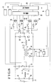
- the series resonant power converter shown in Fig. 4 includes a first circuit in which the first main switch means 1 and the second main switch means each consisting of FET are connected in series with each other in a forward direction, a second circuit in which the diodes 3 and 4 are connected in series with each other in a forward direction and a third circuit in which the resonant capacitors 5 and 6 are connected in series with each other, and the DC input power source 7 is connected across these circuits.
- the main switch means 1 and 2 are arranged in the forward direction relatively to the DC input power source 7, while the diodes 3 and 4 have an opposite polarity to that of the DC power source.
- the tank circuit 10 consists of a parallel circuit including the resonant reactor 8 and the resonant capacitor 9, and a series circuit including said tank circuit 10, the primary winding of the main transformer 11, and the resonant reactor 12 is connected between said juncture of the diodes 3, 4 and the resonant capacitors 5, 6 and the juncture of the switch means 1 and 2.
- the output capacitor 15 and the load 16 are connected through the diodes 13 and 14 to the secondary winding of the main transformer 11.
- a detecting point a for detecting the DC input voltage V a with reference to the negative terminal of the DC input power source 7, a detecting point b for detecting the resonant voltage V b , that is, the voltage at the juncture of the tank circuit 10 and the primary winding of the main transformer 11, and a detecting point c for detecting the DC output voltage V c , that is, the voltage across the load 16, are connected to the control circuit 20, through the voltage detectors 17, 18 and 19, respectively.
- the current detector 21 which is arranged in a current path of the resonant reactor 8 and serves to detect the current through said resonant reactor 8 in the direction as indicated by an arrow, is connected to the control circuit 20.
- the driving circuit 22 is connected with the control circuit 20 to receive a signal therefrom.
- This driving circuit 22 is so arranged that it feeds ON and OFF signals to the main switch means 1 through the transformers 23 and 24, respectively, while it feeds ON and OFF signals to the main switch means 2 through the transformers 25 and 26, respectively.
- the switch means 27 - 30 consisting of transistors, diodes or the like are arranged to turn ON only when the signals are fed thereto, synchronous with the signals fed from the transformers 23 - 30.
- the control circuit 20 is arranged to feed control signals to the driving circuit 22 and drives the main switch means 1 or 2 in the manner as hereinafter described. That is, the control circuit 20 is constituted to generate an ON signal (output power control signal S1, S1′) which acts to produce a required output power, a signal which acts to turn ON the main switch means at the time when the voltage computed by the means for detecting and computing the voltage applied across the main switch means drops to a minimum voltage required to sustain the oscillation of the converter, and a signal (current state control signal S4, S4′) which acts to turn OFF the main switch means at the time when the current through the parallel resonant tank circuit is detected to be zero.
- an ON signal output power control signal S1, S1′
- S4′ current state control signal
- These signals operate in such manner that a signal fed at a former time acts with priority to a signal fed at a later time in the same period, and within the same period a plurality of ON driving operations of the same main switch means 1 or 2 are inhibited.
- the control circuit feeds an OFF signal (S3, S3′) which acts to turn OFF the main switch means 1 or 2.
- the OFF signal S3, S3′ is produced when the current through the main switch means 1 or 2 is detected to drop to a zero value.
- the measure of producing the OFF signal S3, S3′ has been well known in the art and, therefore, a detailed description thereof is omitted.
- the main switch means 1 is turned ON, so that the charging current flows from the DC input power source 7 through the main switch means 1 ⁇ the resonant reactor 12 ⁇ the primary winding of the main transformer 11 ⁇ the tank circuit 10 to the resonant capacitor 6 and at the same time the discharging current flows through the main switch means 1 ⁇ the resonant reactor 12 ⁇ the primary winding of the main transformer 11 ⁇ the tank circuit 10 to the resonant capacitor 5.
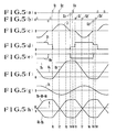
- This current is a resonant current I1 which serves to discharge the resonant capacitor 5 and to charge the resonant capacitor 6. If the direction indicated by an arrow in Fig. 4 is assumed to be positive, the current is as shown in Fig.
- the drain-source voltage of the main switch means is shown in Fig. 5(d)
- the anode voltage of the diode 14 (cathode is grounded) is shown in Fig. 5(e)
- the voltage V c which is conversed to a value of electromotive force at the primary winding of the main transformer from the detected voltage V a at the detecting point a
- the detected voltage V b at the detecting point b and the detected voltage V c at the detecting point c is shown in Fig. 5(f)
- the detected current I L of the current detector 21 is shown in Fig. 5(g).
- the values of these voltages will be hereinafter described.
- a predetermined voltage K and wave forms of voltages representing results of computation of (V a - V b - V c ) and (V b - V c ) are shown in Fig. 5(h).
- the voltage state control signal S2 which acts to turn ON the main switch means 1, is generated, but this signal is neglected under the function of inhibiting a plurality of ON-operations of the same main switch means within the same time period.
- the diode 3 becomes conductive at once, and the current I1 flowing through the resonant reactor 12 flows from the resonant reactor 12 through the primary winding of the main transformer 11 ⁇ the tank circuit 10 ⁇ the diode 3 ⁇ the main switch means 1.
- This current I1 is consumed by the load 16 through the diode 14 and it becomes zero at the time t4.
- the OFF signal S3 is applied to the main switch means 1.
- the value of the current detected by the current detector 21 becomes zero, at which the current changes from negative value to a positive value.
- the current state detecting signal S4 which acts to turn ON the main switch means 1, is generated, but it is neglected under the function of inhibiting a plurality of ON-operations of the same main switch means within the same period. Thus, a half cycle of operation terminates.
- the output power control signal S1′ as shown in Fig. 5(b) is applied to the main switch means 2. Then the main switch means 2 is turned ON, so that the resonant capacitor 5 is charged and the resonant capacitor 6 is discharged. The same operation as described with reference to the first half cycle is performed and the second half cycle terminates.
- the predetermined value K corresponds to a value of the voltage applied to said switch means 1 or 2 immediately before the main switch means 1 or 2 is turned ON by the voltage state control signal S2 or S2′ minus a value conversed to the primary side from the output voltage.
- This value K must meet such relationship in potential that a current flows when the main switch means 1 or 2 is turned ON and, consequently, it must have a positive value.
- this value falls within a range where the oscillation can be sustained, it is desirable to reduce this value, because the smaller is this value, the closer is the operating frequency to the parallel resonant frequency of the tank circuit 10, so that the current at the breeder resistance can be minimized.
- both of the output power control signals S1, S1′ and the voltage state control signals S2, S2′ are not generated, but at the time t5 or t10 where the resonant current I1 flowing through the resonant reactor 8 becomes zero in the process of changing from negative to positive or from positive to negative, the current state control signal S4, S4′ is applied to the main switch means 1 or 2 to cause the main switch means 1 or 2 to be turned ON.
- the oscillating frequency of the tank circuit 10 lowers toward the parallel resonant frequency, so that the operating frequency is decreased and the amplitude of the voltage of the tank circuit 10 itself is increased accordingly, until the output power control signal S1, S1′ operates with priority to the voltage state control signal S2, S2′ and for a while the output power control signal S1, S1′ operates, whereby the steady-state operation is restored.
- the output power control signal S1, S1′ operates with priority to the voltage state control signal S2, S2′ and for a while the output power control signal S1, S1′ operates, whereby the steady-state operation is restored.
- Fig. 6 illustrates a fourth embodiment of the present invention.
- the circuit is so arranged that the resonant capacitors 5 and 6 also perform a function of the resonant capacitor 9 as shown in Fig. 4.
- the input capacitors 31 and 32 act to divide a potential of the DC input power source 7.
- the method of controlling the series resonant converter of this embodiment is substantially same as explained with reference to the embodiment shown in Fig. 4.
- the technical effect obtained is also substantially same as explained with reference to Fig. 4.
- Fig. 7 illustrates a fifth embodiment of the present invention.
- the diodes 33 and 34 are connected in parallel with the main switch means 1 and 2 but with opposite polarities with respect thereto.
- the method of controlling the series resonant converter of this embodiment is substantially same as explained with reference to the embodiment shown in Fig. 4 and the technical effect obtained in the former is substantially same as in the latter.
- Fig. 8 illustrates a sixth embodiment of the present invention.
- the circuit arrangement of this embodiment corresponds to a combination of embodiments of Figs. 6 and 7.
- the method controlling the converter and the technical effect of the embodiment shown in Fig. 8 are substantially same as those explained with reference to the embodiment shown in Fig. 4.
Abstract
Description
- The present invention relates to a series resonant power converter for producing a desired DC voltage for a load, and a method of controlling such series resonant converter.
- In general, a value of a resonant current of a series resonant converter depends on values of an inductance of a resonant reactor, a capacitance of a resonant capacitor, a DC input voltage and a DC output voltage. Accordingly, many researches have been made on a relationship between these values and the resonant current. As the result of these researches, it has been found that in order to control the output voltage of the series resonant power converter at a constant voltage, without controlling the value of the output current, it is necessary to adjust the value of the output current (average value of the resonant current) by control of OFF-periods of a main switch means (that is, frequency control). However, in the case where the constant voltage control of the power converter is effected by the frequency control method, such problem arises that an operating frequency of the converter, which is in proportional relation to the output current, may drop to an audible range under a light load condition (in the case of less output current), with the result that a noise is produced.
- In order to solve such problem, it has been proposed to provide a series resonant converter, as shown in Fig. 3, in which a tank circuit consisting of parallel resonant circuits having an infinite impedance at its resonant frequency is inserted in the series resonant circuit loop, whereby an impedance of the resonant circuit is increased under a light load condition and thus the load dependent characteristic of the operating frequency is minimized.
- Now, the series resonant power converter according to a prior art will be explained, with reference to Fig. 3. The series resonant converter shown in Fig. 3 includes a
first circuit 13 having switch means 11 and 12, such as bipolar transistors, connected together in series in forward direction, asecond circuit 16 havingdiodes third circuit 19 havingresonant capacitors DC power source 21 connected across both ends of these circuits. The switch means 11 and 12 are arranged in forward direction relatively to theDC power source 21 but thediodes diodes resonant capacitors fourth circuit 24 is connected between thejuncture 22 of theresonant capacitors juncture 23 of the switch means 11 and 12. Thefourth circuit 24 includes arectifying circuit 25, aresonant inductor 26 and atank circuit 27, which are connected in series with each other, and saidtank circuit 27 consists of a parallel circuit including aresonant inductor 28 and aresonant capacitor 29. The rectifyingcircuit 25 consists of a bridge circuit including diodes 31 - 34. Anoutput capacitor 35 is connected across output terminals of said bridge circuit and aload 36 is connected in parallel with saidoutput capacitor 35. - Now, the operation of the above series resonant power converter will be explained.
- As an initial condition, it is assumed that the
resonant capacitor 17 has been charged up to a voltage of theDC power source 21 and theresonant capacitor 18 has been discharged to a zero voltage. Under such condition, if thesemiconductor switch 11 is turned ON, a current i₁ flows from theDC power source 21 → thesemiconductor switch 11 → thediode 31 of the rectifyingcircuit 25 → the load 36 (capacitor 35) → thediode 33 of the rectifyingcircuit 25 → theresonant inductor 26 → thetank circuit 27 to theresonant capacitor 18. At the same time, a discharging current i₂ flows from the switch means 11 → thediode 31 of the rectifyingcircuit 25 → the load 36 (capacitor 35) → thediode 33 of the rectifyingcircuit 25 → theresonant inductor 26 → thetank circuit 27 to theresonant capacitor 17. This current is a resonant current which discharges theresonant capacitor 17 and charges theresonant capacitor 18. The capacitance Cp of thecapacitor 29 is set at a value higher than the capacitance Cs of the resonant capacitor 17 (or the resonant capacitor 18), so that the voltage of theresonant capacitor 17 becomes zero and the voltage of theresonant capacitor 18 becomes equal to the power source voltage Vi, after the lapse of about √2 Ls·Cs {π - cos⁻¹ (Vo/(Vi-Vo))} sec, where Vo is a voltage (output voltage) of theoutput capacitor 35, Ls is an inductance of theresonant inductor 26 and Vi is a voltage of theDC power source 21. At this moment, thediode 14 becomes conductive and the current which has passed through theresonant inductor 26, flows as the current i₂ from theresonant inductor 26 → thetank circuit 27 → thediode 14 → the switch means 11 → the rectifyingcircuit 25 → the load 36 (capacitor 35) → the rectifyingcircuit 25. This current i₂ is consumed by theload 36, until it becomes zero. - Thus a half cycle of the operation terminates. Then, if the switch means 12 is turned ON, the
resonant capacitor 17 is charged while theresonant capacitor 18 is discharged and the similar operation as described above occurs. Thus the next half cycle terminates. - The resonant frequency f₁ of the parallel
resonant tank circuit 27 consisting of the capacitance Cp of thecapacitor 29 and the inductance Lp of theinductor 28 is expressed by the following equation:
f₁ = (2π √Lp·Cp )⁻¹ (1),
and the resonant frequency f₀ of the series resonant circuit consisting of the capacitance Cs of the resonant capacitor 17 (or the capacitor 18) and the inductance Ls of theresonant inductor 26 is expressed by the following equation:
f₀ = (2π √Ls·Cs )⁻¹ (2). - With regard to the above resonant frequencies f₁ and f₀, it is required for them to satisfy the following relationship:
f₁ < < f₀ (3) - To meet such requirement, f₀ is set at a value substantially lower than f₁ and the impedance of the
tank circuit 27 is increased at around f₁, so that the minimum operating frequency of the converter is clamped at f₀. That is, the operating frequency of the converter should be controlled to be increased so that it becomes higher than an audible range, thereby preventing noise scattering. - On the other hand, to reduce the output current, the operating frequency of the converter should be controlled to be decreased. Under such circumstances, it has been a usual practice to generate parallel resonance in the
tank circuit 27 so that the converter can operate under excessively light load and to restrict the input current of the converter to feed only less output current. By using such additional parallel resonant tank circuit, it is possible to operate the converter with good result even under light load condition, without the need of lowering the operating frequency of the converter to the audible frequency range. In general, in order to hold the output voltage or the output current at constant, it is usual to detect a variation thereof thereby automatically controlling the operating frequency. - The converter according to the prior art, as described above, poses some problems to be solved.
- Firstly, in the circuit of the series resonant converter according to the prior art, in order to simultaneously satisfy the requirements as expressed by (1), (2) and (3), the capacitance of the
resonant capacitor 29 in the parallelresonant tank circuit 27 must have a high value, at least four to five times as high as that of theresonant capacitor resonant circuit 27 must have a value corresponding to Q times as high as the energy transmitted to the output side, where Q is the Q factor of the parallel resonant tank circuit. Accordingly, the resonant inductor used must be of large size, with the result that the power dissipation is increased. Furthermore, it is necessary to separately provide a resonant capacitor having a large capacitance, for thetank circuit 27. - Secondly, in the control method for controlling the series resonant power converter according to the prior art, in the case where a negative feedback is applied to the series resonant converter to control its output power, a temporary interruption of the wave form may happen at a transient time responsive to starting of operation, variation of the load condition, variation of input voltage or the like and the operating frequency may drop below the parallel resonant frequency of said tank circuit. In such cases, the impedance of the series resonant circuit loop drops when the operating frequency varies beyond the parallel resonant frequency of said tank circuit, so that the converter is operated in undesirable positive feedback operation rather than negative feedback operation and it becomes impossible to effect a stable control of the converter.
- It is an object of the present invention to eliminate the disadvantages of the circuit of the series resonant converter according to the prior art.
- In accordance with the present invention there is provided a series resonant circuit which comprises a first circuit including a first switch means and a second switch means connected in series with each other in a forward direction; a second circuit including a first diode and a second diode connected in series with each other in a forward direction; a third circuit including a first resonant capacitor and a second resonant capacitor connected in series with each other; a DC power source connected across both ends of said first, second and third circuits; a first resonant inductor connected in a path of a main current flowing through said first switch means or said second switch means, said first resonant inductor being connected, at its one end, to a juncture of said first switch means with said second switch means and, at its other end, to a juncture of said first diode and said second diode and a juncture of said first resonant capacitor with said second resonant capacitor; and a second resonant inductor connected, at its one end, to the juncture of said first diode with said second diode and the juncture of said first resonant capacitor with said second capacitor and, at its other end, to a neutral potential point of said DC power source.
- According to this invention, the resonant capacitor is commonly used in the series resonant circuit and the parallel resonant circuit and the capacitance of the resonant capacitor can be considerably decreased, as compared with the one used in the conventional tank circuit, so that the energy handled by the resonant capacitor can be decreased. Accordingly, the size of the resonant inductor can be decreased and the power loss can be minimized.
- Furthermore in accordance with the present invention there is provided a method of controlling a series resonant converter including a first resonant circuit consisting of one of a first main switch means and a second main switch means which is in ON-state and a main transformer, and a second resonant circuit, in which ON-OFF operation of the first or second main switch means is controlled by an output power control signal, to produce a predetermined DC output power, said method comprising: a step of causing said first or second main switch means to be turned ON by a voltage state detecting signal, thereby avoiding temporary interruption of wave form and sustaining oscillating operation, when a value conversed to a primary side from a value of a voltage applied across said first or second main switch means minus an output voltage drops below a reference voltage (K), in the case where the above-mentioned output control signal has not been generated at a transient time owing to variation of the load condition, variation of input voltage or the like.
- According to this invention, the series resonant converter as described above includes means for detecting and computing a voltage applied across the main switch means when it is in OFF-state, and a control circuit which is arranged to cause the main switch means to be driven at the time when the voltage computed as above becomes a minimum voltage required to sustain the oscillation of the series resonant converter. This minimum voltage can be computed by a detecting circuit for detecting the input voltage, a detecting circuit for detecting a voltage of the second resonant circuit and a detecting circuit for detecting a DC output voltage conversed to a primary side of the main transformer.
- According to this method of controlling the series resonant converter, the temporary interruption of the operating wave form which may happen at a transient time responsive to starting of operation, variation of the load condition, variation of input voltage can be avoided, and the stable control of the converter can be obtained.
- Now, the invention will be explained with reference to the drawings.
-
- Fig. 1 illustrates an embodiment of the series resonant converter according to the present invention.
- Fig. 2 illustrates another embodiment of the series resonant circuit according to the present invention.
- Fig. 3 illustrates a series resonant converter according to a prior art.
- Figs. 4 and 5 illustrate another embodiment of the present invention.
- Figs. 6 - 8 illustrate further embodiments of the present invention, respectively.
- Firstly a description will be given to the embodiment of the present invention as illustrated in Fig. 1.
- In Fig. 1, any components corresponding to those shown in Fig. 3, which illustrates the prior art, are indicated by same numerals as used in Fig. 3.
- In Fig. 1, 11 and 12 indicate main switch means; 13 indicates a first circuit; 14 and 15 indicate diodes; 16 indicates a second circuit; 17 and 18 indicate resonant capacitors; 19 indicates a third circuit; 21 indicates a DC power source; 26 and 28 indicate resonant inductors; and 40 indicates a transformer.
- In the series resonant power converter as shown in Fig. 1, the
resonant inductor 28 is connected, at its one end, to a point A, which forms a juncture between thediodes second circuit 16 and a juncture between theresonant capacitors third circuit 19 and, at its other end, to a neutral voltage point B of theDC power source 21. Theresonant capacitors resonant inductor 18, and these resonant capacitor produce series resonance with theresonant inductor 26, respectively. Thus the main current flowing through thefirst circuit 13 flows through thethird circuit 19. - The operation of the above circuit is substantially same as that of the circuit according to the prior art as described above. Now, it is assumed that the switch means 11 is turned ON. Then, a charging circuit from the
DC power source 21 through the switch means 11 → a primary winding of thetransformer 40 → theresonant inductor 26 → the juncture A to theresonant capacitor 18 is formed. At the same time, a discharging circuit from the switch means 11 through the primary winding of thetransformer 40 → theresonant inductor 26 to theresonant capacitor 17 is formed. The charging current serves to charge theresonant capacitor 18 up to substantially the source voltage, and after theresonant capacitor 17 has discharged to substantially zero voltage, thediode 14 of thesecond circuit 16 becomes conductive and the energy accumulated at theresonant inductor 16 is transferred through thediode 14 → switch means 11 →transformer 40 to the output side. After the OFF period of the switch means 11 and 12, the switch means 12 is turned ON. The ON operation of the switch means 12 is same as that of the switch means 11 and so the detailed description thereof is omitted. - The
diodes resonant capacitors third circuit 19, respectively, and consequently they are not adversely affected by the recovery of thediodes - Even during the period when both of the switch means 11 and 12 are in OFF-state, the
resonant capacitors resonant inductor 28 generate oscillation at a natural frequency, thereby oscillating the voltage at the juncture A. Under light load condition, the switch means 11 or 12 is turned ON under a state of voltage at the juncture A where a voltage across the switch means 11 or 12 is of a lower voltage (a voltage having small amplitude corresponding to the voltage of theDC power source transformer 40 is decreased. As the switching frequency of the switch means 11 and 12 comes closer to the parallel resonant frequency of theresonant capacitor resonant inductor 28, the amplitude of the voltage oscillation becomes larger. Accordingly, under light load condition, the switch means 11 or 12 is switched at a frequency near the above-mentioned parallel resonant frequency. - Under a rated load condition, the switch means 11 and 12 are subjected to switch operation at a considerably higher frequency than the above-mentioned parallel resonant frequency, so that the amplitude of the oscillation of voltage at the juncture A is small. Accordingly the amplitude of the value of the voltage corresponding to the voltage of the
DC power source transformer 40 is high. - As explained above, according to the embodiment of the present invention, the resonant capacitor is commonly used in the parallel resonant circuit and the series resonant circuit and the capacitance of said resonant capacitor can be considerably small, as compared to the resonant capacitor used in the tank circuit according to the prior art. Accordingly the energy dissipated by the resonant capacitor can be substantially decreased, so that it is unnecessary to provide a separate resonant capacitor for the parallel resonant circuit, while the size of the resonant inductor can be decreased and the power loss can be decreased.
- Fig. 2 illustrates a modified embodiment of the present invention. According to the embodiment as shown in Fig. 2, the
power source 21′ consists of a three-phasefull wave rectifier 21′, achoke 43 andcapacitors 41 and 42. Thecapacitors 41 and 42 with thechoke 43 constitute a filter circuit and substantially half of the DC source voltage is applied to a neutral potential point B. In usual, thecapacitors 41 and 42 are designed to have a large capacitance value, which is larger than 10 times as large as that of theresonant capacitor 41 or 42. - Figs. 4 and 5 illustrate another embodiment of the present invention. Figs. 6 - 8 illustrate further embodiments of the present invention, respectively. In these figures, 1 indicates a main switch means; 2 indicates a second switch means; 3, 4, 13, 14, 33 and 34 indicate diodes; 5, 6 and 9 indicate resonant capacitors; 7 indicates a DC input power source; 8 and 12 indicate resonant reactors; 10 indicates a tank circuit; 11 indicates a main transformer; 15 indicates an output capacitor; 16 indicates a load; 17, 18 and 19 indicate a voltage detector; 20 indicates a control circuit; 21 indicates a current detector; 22 indicates a driving circuit; 23 - 26 indicate a transformer; 27 - 30 indicate a switch means; and 31 and 32 indicate an input capacitor.
- The series resonant power converter shown in Fig. 4 includes a first circuit in which the first main switch means 1 and the second main switch means each consisting of FET are connected in series with each other in a forward direction, a second circuit in which the
diodes resonant capacitors 5 and 6 are connected in series with each other, and the DC input power source 7 is connected across these circuits. The main switch means 1 and 2 are arranged in the forward direction relatively to the DC input power source 7, while thediodes diodes resonant capacitors 5 and 6 are connected together. Thetank circuit 10 consists of a parallel circuit including theresonant reactor 8 and theresonant capacitor 9, and a series circuit including saidtank circuit 10, the primary winding of themain transformer 11, and theresonant reactor 12 is connected between said juncture of thediodes resonant capacitors 5, 6 and the juncture of the switch means 1 and 2. Theoutput capacitor 15 and theload 16 are connected through thediodes main transformer 11. A detecting point a for detecting the DC input voltage Va with reference to the negative terminal of the DC input power source 7, a detecting point b for detecting the resonant voltage Vb, that is, the voltage at the juncture of thetank circuit 10 and the primary winding of themain transformer 11, and a detecting point c for detecting the DC output voltage Vc, that is, the voltage across theload 16, are connected to thecontrol circuit 20, through thevoltage detectors current detector 21, which is arranged in a current path of theresonant reactor 8 and serves to detect the current through saidresonant reactor 8 in the direction as indicated by an arrow, is connected to thecontrol circuit 20. The drivingcircuit 22 is connected with thecontrol circuit 20 to receive a signal therefrom. This drivingcircuit 22 is so arranged that it feeds ON and OFF signals to the main switch means 1 through thetransformers transformers - The
control circuit 20 is arranged to feed control signals to the drivingcircuit 22 and drives the main switch means 1 or 2 in the manner as hereinafter described. That is, thecontrol circuit 20 is constituted to generate an ON signal (output power control signal S₁, S₁′) which acts to produce a required output power, a signal which acts to turn ON the main switch means at the time when the voltage computed by the means for detecting and computing the voltage applied across the main switch means drops to a minimum voltage required to sustain the oscillation of the converter, and a signal (current state control signal S₄, S₄′) which acts to turn OFF the main switch means at the time when the current through the parallel resonant tank circuit is detected to be zero. These signals operate in such manner that a signal fed at a former time acts with priority to a signal fed at a later time in the same period, and within the same period a plurality of ON driving operations of the same main switch means 1 or 2 are inhibited. Also, the control circuit feeds an OFF signal (S₃, S₃′) which acts to turn OFF the main switch means 1 or 2. The OFF signal S₃, S₃′ is produced when the current through the main switch means 1 or 2 is detected to drop to a zero value. The measure of producing the OFF signal S₃, S₃′ has been well known in the art and, therefore, a detailed description thereof is omitted. - Now the operation of the power converter as shown in Fig. 4 will be described. As an initial condition, it is assumed that the
resonant capacitor 5 has been charged up to the voltage of the DC input power source 7 and the resonant capacitor 6 has been discharged to the zero voltage and the operation will be explained with reference to Fig. 5. Under this condition and when the output power control signal S₁ as shown in Fig. 5(a) is applied to the main switch means 1 at the time t₁, the main switch means 1 is turned ON, so that the charging current flows from the DC input power source 7 through the main switch means 1 → theresonant reactor 12 → the primary winding of themain transformer 11→ thetank circuit 10 to the resonant capacitor 6 and at the same time the discharging current flows through the main switch means 1 → theresonant reactor 12 → the primary winding of themain transformer 11 → thetank circuit 10 to theresonant capacitor 5. This current is a resonant current I₁ which serves to discharge theresonant capacitor 5 and to charge the resonant capacitor 6. If the direction indicated by an arrow in Fig. 4 is assumed to be positive, the current is as shown in Fig. 5(c). Referring to Fig. 5, the drain-source voltage of the main switch means is shown in Fig. 5(d), the anode voltage of the diode 14 (cathode is grounded) is shown in Fig. 5(e), the voltage Vc which is conversed to a value of electromotive force at the primary winding of the main transformer from the detected voltage Va at the detecting point a, the detected voltage Vb at the detecting point b and the detected voltage Vc at the detecting point c is shown in Fig. 5(f), and the detected current IL of thecurrent detector 21 is shown in Fig. 5(g). The values of these voltages will be hereinafter described. A predetermined voltage K and wave forms of voltages representing results of computation of (Va - Vb - Vc) and (Vb - Vc) are shown in Fig. 5(h). When the voltage (Va - Vb - Vc) drops to the predetermined voltage K at the time t₂, the voltage state control signal S₂, which acts to turn ON the main switch means 1, is generated, but this signal is neglected under the function of inhibiting a plurality of ON-operations of the same main switch means within the same time period. When the voltage of theresonant capacitor 5 becomes zero and the voltage of the resonant capacitor 6 becomes the voltage of the DC input power source 7, at the time t₃, thediode 3 becomes conductive at once, and the current I₁ flowing through theresonant reactor 12 flows from theresonant reactor 12 through the primary winding of themain transformer 11 → thetank circuit 10 → thediode 3 → the main switch means 1. This current I₁ is consumed by theload 16 through thediode 14 and it becomes zero at the time t₄. At the time t₄ when the current I₁ becomes zero, the OFF signal S₃ is applied to the main switch means 1. At the time t₅, the value of the current detected by thecurrent detector 21 becomes zero, at which the current changes from negative value to a positive value. At this time t₅, the current state detecting signal S₄, which acts to turn ON the main switch means 1, is generated, but it is neglected under the function of inhibiting a plurality of ON-operations of the same main switch means within the same period. Thus, a half cycle of operation terminates. At the time t₆, the output power control signal S₁′ as shown in Fig. 5(b) is applied to the main switch means 2. Then the main switch means 2 is turned ON, so that theresonant capacitor 5 is charged and the resonant capacitor 6 is discharged. The same operation as described with reference to the first half cycle is performed and the second half cycle terminates. In the second half cycle, when the voltage (Vb - Vc) drops to the above-mentioned predetermined voltage K at the time t₇, the voltage state control signal S₂′, which acts to turn ON the main switch means 2, is produced, but this signal is neglected under the function of inhibiting a plurality of operations of the same main switch means within the same period. Under such steady-state operating condition, the operation of detecting the output voltage and applying the detected voltage to the main switch means 1 or 2 is repeated, whereby the operating frequency is automatically controlled to maintain the constant output voltage. - Under the above-mentioned steady-state operating conditiing if a variation of the load arises to change light (the output current is decreased), for example, it becomes necessary to lower the operating frequency and the output power control signals S₁ and S₁′ is temporarily stopped. However, in the embodiment as described above, at the time t₂ when (Va - Vb - Vc) drops to the predetermined voltage value K, the voltage state control signal S₂ is applied to the main switch means 1, whereby the main switch means 1 and 2 are operated so that the main switch means 2 is turned ON, and thus even during the transient time where the output power control signals S₁ and S₁′ are not produced, the temporary interruption of the wave form is avoided, so that the negative feedback state is maintained and the stable control can be effected.
- The predetermined value K, referred to in the above description, corresponds to a value of the voltage applied to said switch means 1 or 2 immediately before the main switch means 1 or 2 is turned ON by the voltage state control signal S₂ or S₂′ minus a value conversed to the primary side from the output voltage. This value K must meet such relationship in potential that a current flows when the main switch means 1 or 2 is turned ON and, consequently, it must have a positive value.
- If this value falls within a range where the oscillation can be sustained, it is desirable to reduce this value, because the smaller is this value, the closer is the operating frequency to the parallel resonant frequency of the
tank circuit 10, so that the current at the breeder resistance can be minimized. - Under a transient state where a usual variation occurs, the oscillation is sustained by the operation of the above-mentioned voltage state control signals S₂, S₂′ until the output power control signal S₁, S₂ comes into operation, whereby the steady-state operation can be restored. However, in the case where a considerable variation in the load arises, for example, a variation arises from a heavy load to a light load (and the current considerably decreases accordingly), it is probable that the voltage does not drop to the predetermined voltage K, because of small amplitude of the
tank circuit 10 itself and, consequently, small amplitude of the voltage (Va - Vb - Vc) and the voltage (Vb - Vc). In such case, both of the output power control signals S₁, S₁′ and the voltage state control signals S₂, S₂′ are not generated, but at the time t₅ or t₁₀ where the resonant current I₁ flowing through theresonant reactor 8 becomes zero in the process of changing from negative to positive or from positive to negative, the current state control signal S₄, S₄′ is applied to the main switch means 1 or 2 to cause the main switch means 1 or 2 to be turned ON. At this time, the oscillating frequency of thetank circuit 10 lowers toward the parallel resonant frequency, so that the operating frequency is decreased and the amplitude of the voltage of thetank circuit 10 itself is increased accordingly, until the output power control signal S₁, S₁′ operates with priority to the voltage state control signal S₂, S₂′ and for a while the output power control signal S₁, S₁′ operates, whereby the steady-state operation is restored. Thus, even in a transient state where both of the output power control signals S₁, S₂ and the voltage state control signal S₂, S₂′ are not generated, temporary interruption of a wave form is avoided, so that the negative feedback state is maintained and the stable control of the converter is assured. - In the above descriptions, the present invention is explained with reference to the embodiments where the invention is applied to the constant output voltage control. The present invention can be also applied to a constant current control. Such embodiment will be hereinafter described.
- Fig. 6 illustrates a fourth embodiment of the present invention. In Fig. 6, the circuit is so arranged that the
resonant capacitors 5 and 6 also perform a function of theresonant capacitor 9 as shown in Fig. 4. Theinput capacitors - Fig. 7 illustrates a fifth embodiment of the present invention. In this embodiment, the
diodes - Fig. 8 illustrates a sixth embodiment of the present invention. The circuit arrangement of this embodiment corresponds to a combination of embodiments of Figs. 6 and 7. The method controlling the converter and the technical effect of the embodiment shown in Fig. 8 are substantially same as those explained with reference to the embodiment shown in Fig. 4.
Claims (4)
a first circuit including a first switch means and a second switch means connected in series with each other in a forward direction;
a second circuit including a first diode and a second diode connected in series with each other in a forward direction;
a third circuit including a first resonant capacitor and a second resonant capacitor connected in series with each other;
a DC power source connected across both ends of said first, second and third circuits;
a first resonant inductor connected in a path of a main current flowing through said first switch means or said second switch means, said first resonant inductor being connected, at its one end, to a juncture of said first switch means with said second switch means and, at its other end, to a juncture of said first diode and said second diode and a juncture of said first resonant capacitor with said second resonant capacitor; and
a second resonant inductor connected, at its one end, to the juncture of said first diode with said second diode and the juncture of said first resonant capacitor with said second capacitor and, at its other end, to a neutral potential point of said DC power source.
including a first resonant circuit consisting of one of a first main switch means or a second main switch means, one of which is in ON-state and a main transformer, a second resonant circuit, rectifying means for producing a DC output power from a secondary winding of said main transformer and a control circuit for controlling ON-OFF operation of said first or second main switch means, wherein, said control circuit comprises a circuit for driving said first or second main switch means to its OFF-state in order to generate a required DC output power;
a circuit for detecting a current flowing through said first or second main switch means and for driving said first or second switch means to its OFF-state at the time when the detected current becomes zero;
a circuit for detecting a current flowing through said second resonant circuit and for driving said first or second main switch means to its OFF-state at the time when said current flowing through said second main switch becomes zero; and
a circuit having means for detecting and computing a voltage applied across said first or second main switch means and arranged to drive said first or second main switch means to ON-state at the time when said detected and computed voltage drops to a minimum voltage required to sustain oscillation of the series resonant power converter.
a detecting circuit for detecting an input voltage;
a detecting circuit for detecting a voltage of said second resonant circuit;
a detecting circuit for detecting a DC output voltage conversed into an electromotive force at the primary side of said main transformer; and
a computing circuit for computing these voltages.
a step of causing said first or second main switch means to be turned ON by a voltage state detecting signal, thereby avoiding temporary interruption of wave form to sustain oscillating operation, when a value conversed to a primary side from a value of a voltage applied across said first or second main switch means minus a value of an output voltage drops below a reference voltage (K), in the case where the above-mentioned output control signal has not been generated at a transient time owing to variation of load condition, variation of input voltage or the like.
Applications Claiming Priority (4)
| Application Number | Priority Date | Filing Date | Title |
|---|---|---|---|
| JP57934/88 | 1988-03-11 | ||
| JP5793488A JPH0648902B2 (en) | 1988-03-11 | 1988-03-11 | Control method of series resonant converter |
| JP63098695A JPH0650946B2 (en) | 1988-04-21 | 1988-04-21 | Series resonant converter |
| JP98695/88 | 1988-04-21 |
Publications (3)
| Publication Number | Publication Date |
|---|---|
| EP0332436A2 true EP0332436A2 (en) | 1989-09-13 |
| EP0332436A3 EP0332436A3 (en) | 1990-06-27 |
| EP0332436B1 EP0332436B1 (en) | 1996-06-05 |
Family
ID=26399022
Family Applications (1)
| Application Number | Title | Priority Date | Filing Date |
|---|---|---|---|
| EP89302335A Expired - Lifetime EP0332436B1 (en) | 1988-03-11 | 1989-03-09 | Series resonant power converter and method of controlling the same |
Country Status (4)
| Country | Link |
|---|---|
| US (1) | US5075836A (en) |
| EP (1) | EP0332436B1 (en) |
| CA (1) | CA1318349C (en) |
| DE (1) | DE68926585T2 (en) |
Cited By (3)
| Publication number | Priority date | Publication date | Assignee | Title |
|---|---|---|---|---|
| EP0518300A1 (en) * | 1991-06-11 | 1992-12-16 | Yamaha Corporation | Power supply circuit |
| EP1248356A2 (en) * | 2001-04-06 | 2002-10-09 | Philips Corporate Intellectual Property GmbH | Power supply circuit with a DC/DC-converter |
| WO2009154489A1 (en) * | 2008-06-20 | 2009-12-23 | Akademia Gorniczo-Hutnicza Im. Stanislawa Staszica | Multi-resonance power supply with an integral quality factor limiter |
Families Citing this family (12)
| Publication number | Priority date | Publication date | Assignee | Title |
|---|---|---|---|---|
| US5196775A (en) * | 1991-02-20 | 1993-03-23 | Honeywell Inc. | Switched reluctance motor position by resonant signal injection |
| DE4334592C1 (en) * | 1993-10-11 | 1994-07-21 | Siemens Ag | High frequency generator |
| US5438498A (en) * | 1993-12-21 | 1995-08-01 | Raytheon Company | Series resonant converter having a resonant snubber |
| US5783799A (en) * | 1996-01-11 | 1998-07-21 | Illinois Tool Works Inc. | Series resonant converter, and method and apparatus for control thereof |
| US6124581A (en) * | 1997-07-16 | 2000-09-26 | Illinois Tool Works Inc. | Method and apparatus for producing power for an induction heating source |
| US5909362A (en) * | 1998-01-12 | 1999-06-01 | Eldec Corporation | Resonant power converter |
| DK1124317T3 (en) * | 2000-02-11 | 2005-12-27 | Siemens Magnet Technology Ltd | resonance |
| US6487099B1 (en) | 2001-08-24 | 2002-11-26 | Northrop Grumman Corporation | Time compensated current ramp for resonant power converters |
| US8638571B2 (en) * | 2010-02-19 | 2014-01-28 | Sparq Systems Inc. | Controller for a resonant power converter |
| US8699244B1 (en) * | 2010-10-29 | 2014-04-15 | Universal Lighting Technologies, Inc. | Electronic ballast with load-independent and self-oscillating inverter topology |
| CN103105956B (en) * | 2011-11-11 | 2015-05-06 | 汉王科技股份有限公司 | Position indicating device and position indicating method |
| US9755534B2 (en) * | 2013-02-14 | 2017-09-05 | Nuvolta Technologies, Inc. | High efficiency high frequency resonant power conversion |
Citations (4)
| Publication number | Priority date | Publication date | Assignee | Title |
|---|---|---|---|---|
| EP0201876A2 (en) * | 1985-05-10 | 1986-11-20 | Nippon Telegraph And Telephone Corporation | Series resonant converter |
| EP0231756A1 (en) * | 1986-01-08 | 1987-08-12 | Alsthom | Double resonant inverter |
| US4691273A (en) * | 1986-12-11 | 1987-09-01 | Nippon Telegraph & Telephone Corp. | Series resonant converter with parallel resonant circuit |
| US4727469A (en) * | 1987-03-23 | 1988-02-23 | Reliance Comm/Tec Corporation | Control for a series resonant power converter |
Family Cites Families (2)
| Publication number | Priority date | Publication date | Assignee | Title |
|---|---|---|---|---|
| NL8103474A (en) * | 1981-07-23 | 1983-02-16 | Hollandse Signaalapparaten Bv | ENERGY CONVERTER. |
| AU555174B2 (en) * | 1981-09-18 | 1986-09-18 | Oy Helvar | Electronic ballast for a discharge lamp |
-
1989
- 1989-03-07 CA CA000593007A patent/CA1318349C/en not_active Expired - Lifetime
- 1989-03-09 DE DE68926585T patent/DE68926585T2/en not_active Expired - Lifetime
- 1989-03-09 EP EP89302335A patent/EP0332436B1/en not_active Expired - Lifetime
-
1991
- 1991-01-16 US US07/641,808 patent/US5075836A/en not_active Expired - Lifetime
Patent Citations (4)
| Publication number | Priority date | Publication date | Assignee | Title |
|---|---|---|---|---|
| EP0201876A2 (en) * | 1985-05-10 | 1986-11-20 | Nippon Telegraph And Telephone Corporation | Series resonant converter |
| EP0231756A1 (en) * | 1986-01-08 | 1987-08-12 | Alsthom | Double resonant inverter |
| US4691273A (en) * | 1986-12-11 | 1987-09-01 | Nippon Telegraph & Telephone Corp. | Series resonant converter with parallel resonant circuit |
| US4727469A (en) * | 1987-03-23 | 1988-02-23 | Reliance Comm/Tec Corporation | Control for a series resonant power converter |
Cited By (5)
| Publication number | Priority date | Publication date | Assignee | Title |
|---|---|---|---|---|
| EP0518300A1 (en) * | 1991-06-11 | 1992-12-16 | Yamaha Corporation | Power supply circuit |
| EP1248356A2 (en) * | 2001-04-06 | 2002-10-09 | Philips Corporate Intellectual Property GmbH | Power supply circuit with a DC/DC-converter |
| EP1248356A3 (en) * | 2001-04-06 | 2004-04-21 | Philips Intellectual Property & Standards GmbH | Power supply circuit with a DC/DC-converter |
| WO2009154489A1 (en) * | 2008-06-20 | 2009-12-23 | Akademia Gorniczo-Hutnicza Im. Stanislawa Staszica | Multi-resonance power supply with an integral quality factor limiter |
| US8599578B2 (en) | 2008-06-20 | 2013-12-03 | Akademia Gorniczo-Hutnicza Im. Stanislawa Staszica | Multi-resonance power supply with an integral quality factor |
Also Published As
| Publication number | Publication date |
|---|---|
| DE68926585D1 (en) | 1996-07-11 |
| DE68926585T2 (en) | 1997-02-06 |
| US5075836A (en) | 1991-12-24 |
| EP0332436A3 (en) | 1990-06-27 |
| EP0332436B1 (en) | 1996-06-05 |
| CA1318349C (en) | 1993-05-25 |
Similar Documents
| Publication | Publication Date | Title |
|---|---|---|
| JP3459142B2 (en) | Drive pulse output limiting circuit | |
| US10770979B2 (en) | LLC resonant converter | |
| US4709316A (en) | Single-ended DC-to-DC converter with lossless switching | |
| EP0332436A2 (en) | Series resonant power converter and method of controlling the same | |
| US10903691B2 (en) | Wireless power receiver and wireless power transmission system using the same | |
| US5140510A (en) | Constant frequency power converter | |
| US6788556B2 (en) | Switching power source device | |
| US20040135559A1 (en) | DC to DC converter producing output voltage exhibit rise and fall charactristics independet of load thereon | |
| US20020008981A1 (en) | High frequency sine wave AC Inverter | |
| EP0435459A2 (en) | Mixed mode regulation controller for a resonant power converter | |
| JPH02184267A (en) | Series resonance inverter with non-loss snabber-reset part | |
| US4761727A (en) | Current sensing circuit for use with decoupled half bridge converter | |
| WO1994018748A1 (en) | Control circuit for a switching dc-dc power converter including a controlled magnetic core flux resetting technique for output regulation | |
| US5497310A (en) | High-frequency power unit for neon tubes | |
| US6917528B2 (en) | Switching power transmission device | |
| EP0474312B1 (en) | DC-DC converter | |
| KR960010828B1 (en) | High power factor power supply | |
| EP1739819A1 (en) | Power supply apparatus | |
| EP0271850A2 (en) | Power feeding apparatus | |
| US4945464A (en) | High voltage DC power supply | |
| US5229930A (en) | Welding inverter and method for controlling a welding inverter | |
| JP2003299356A (en) | Dc-dc converter control method | |
| JP2000069750A (en) | Current resonance converter | |
| JP2976603B2 (en) | Series resonant converter control circuit | |
| CN117040255A (en) | Power supply device and laser device |
Legal Events
| Date | Code | Title | Description |
|---|---|---|---|
| PUAI | Public reference made under article 153(3) epc to a published international application that has entered the european phase |
Free format text: ORIGINAL CODE: 0009012 |
|
| AK | Designated contracting states |
Kind code of ref document: A2 Designated state(s): DE FR GB SE |
|
| PUAL | Search report despatched |
Free format text: ORIGINAL CODE: 0009013 |
|
| AK | Designated contracting states |
Kind code of ref document: A3 Designated state(s): DE FR GB SE |
|
| 17P | Request for examination filed |
Effective date: 19900814 |
|
| 17Q | First examination report despatched |
Effective date: 19920730 |
|
| GRAH | Despatch of communication of intention to grant a patent |
Free format text: ORIGINAL CODE: EPIDOS IGRA |
|
| GRAA | (expected) grant |
Free format text: ORIGINAL CODE: 0009210 |
|
| STAA | Information on the status of an ep patent application or granted ep patent |
Free format text: STATUS: THE PATENT HAS BEEN GRANTED |
|
| AK | Designated contracting states |
Kind code of ref document: B1 Designated state(s): DE FR GB SE |
|
| ET | Fr: translation filed | ||
| REF | Corresponds to: |
Ref document number: 68926585 Country of ref document: DE Date of ref document: 19960711 |
|
| PLBE | No opposition filed within time limit |
Free format text: ORIGINAL CODE: 0009261 |
|
| 26N | No opposition filed | ||
| REG | Reference to a national code |
Ref country code: GB Ref legal event code: 746 Effective date: 19990211 |
|
| REG | Reference to a national code |
Ref country code: GB Ref legal event code: IF02 |
|
| PGFP | Annual fee paid to national office [announced via postgrant information from national office to epo] |
Ref country code: SE Payment date: 20080318 Year of fee payment: 20 Ref country code: GB Payment date: 20080318 Year of fee payment: 20 |
|
| PGFP | Annual fee paid to national office [announced via postgrant information from national office to epo] |
Ref country code: DE Payment date: 20080430 Year of fee payment: 20 |
|
| PGFP | Annual fee paid to national office [announced via postgrant information from national office to epo] |
Ref country code: FR Payment date: 20080327 Year of fee payment: 20 |
|
| REG | Reference to a national code |
Ref country code: GB Ref legal event code: PE20 Expiry date: 20090308 |
|
| PG25 | Lapsed in a contracting state [announced via postgrant information from national office to epo] |
Ref country code: GB Free format text: LAPSE BECAUSE OF EXPIRATION OF PROTECTION Effective date: 20090308 |