EP0331689B1 - Connector assembly with diecast housing and drawn shell - Google Patents
Connector assembly with diecast housing and drawn shell Download PDFInfo
- Publication number
- EP0331689B1 EP0331689B1 EP88906794A EP88906794A EP0331689B1 EP 0331689 B1 EP0331689 B1 EP 0331689B1 EP 88906794 A EP88906794 A EP 88906794A EP 88906794 A EP88906794 A EP 88906794A EP 0331689 B1 EP0331689 B1 EP 0331689B1
- Authority
- EP
- European Patent Office
- Prior art keywords
- shell
- housing
- aperture
- diecast
- connector assembly
- Prior art date
- Legal status (The legal status is an assumption and is not a legal conclusion. Google has not performed a legal analysis and makes no representation as to the accuracy of the status listed.)
- Expired - Lifetime
Links
Images


Classifications
-
- H—ELECTRICITY
- H01—ELECTRIC ELEMENTS
- H01R—ELECTRICALLY-CONDUCTIVE CONNECTIONS; STRUCTURAL ASSOCIATIONS OF A PLURALITY OF MUTUALLY-INSULATED ELECTRICAL CONNECTING ELEMENTS; COUPLING DEVICES; CURRENT COLLECTORS
- H01R13/00—Details of coupling devices of the kinds covered by groups H01R12/70 or H01R24/00 - H01R33/00
- H01R13/648—Protective earth or shield arrangements on coupling devices, e.g. anti-static shielding
- H01R13/658—High frequency shielding arrangements, e.g. against EMI [Electro-Magnetic Interference] or EMP [Electro-Magnetic Pulse]
- H01R13/6591—Specific features or arrangements of connection of shield to conductive members
- H01R13/6594—Specific features or arrangements of connection of shield to conductive members the shield being mounted on a PCB and connected to conductive members
-
- H—ELECTRICITY
- H01—ELECTRIC ELEMENTS
- H01R—ELECTRICALLY-CONDUCTIVE CONNECTIONS; STRUCTURAL ASSOCIATIONS OF A PLURALITY OF MUTUALLY-INSULATED ELECTRICAL CONNECTING ELEMENTS; COUPLING DEVICES; CURRENT COLLECTORS
- H01R13/00—Details of coupling devices of the kinds covered by groups H01R12/70 or H01R24/00 - H01R33/00
- H01R13/648—Protective earth or shield arrangements on coupling devices, e.g. anti-static shielding
- H01R13/658—High frequency shielding arrangements, e.g. against EMI [Electro-Magnetic Interference] or EMP [Electro-Magnetic Pulse]
- H01R13/6591—Specific features or arrangements of connection of shield to conductive members
-
- H—ELECTRICITY
- H01—ELECTRIC ELEMENTS
- H01R—ELECTRICALLY-CONDUCTIVE CONNECTIONS; STRUCTURAL ASSOCIATIONS OF A PLURALITY OF MUTUALLY-INSULATED ELECTRICAL CONNECTING ELEMENTS; COUPLING DEVICES; CURRENT COLLECTORS
- H01R12/00—Structural associations of a plurality of mutually-insulated electrical connecting elements, specially adapted for printed circuits, e.g. printed circuit boards [PCB], flat or ribbon cables, or like generally planar structures, e.g. terminal strips, terminal blocks; Coupling devices specially adapted for printed circuits, flat or ribbon cables, or like generally planar structures; Terminals specially adapted for contact with, or insertion into, printed circuits, flat or ribbon cables, or like generally planar structures
Definitions
- This invention relates to an electrical connector assembly and in particular to an electrical connector assembly having a cast housing and drawn shell to provide shielding and a path to ground for the shielding.
- Prior art subminiature D connectors typically had a drawn shell with an integral groundstrap to provide shielding and a conductive path to ground.
- the drawn shell surrounded a thermoplastic housing in which contact terminals were secured and provided shielding therefor, as discloses in US-A-4,679,883.
- a plastic connector body having terminal receiving cavities with terminals secured therein is disposed in a shell.
- a metal commoning spring body having contact fingers aligned with the terminal cavities is also disposed in the shell behind the connector body and the two bodies are locked into the shell by suitable means.
- an electrical connector assembly for mounting on a planar surface, includes an electrically conductive housing having an aperture therein, and a thermoplastic insert having terminal receiving passages, with terminals secured therein, and disposed in the aperture in the housing which thereby provides shielding for the terminals, and is characterized in that the housing comprises a diecast housing having an aperture therein and a drawn shell also having an aperture therein and received in the diecast housing aperture and electrically commoned with the diecast housing, said thermoplastic insert is secured in the shell aperture, and said shell substantially covers the sides of the insert, whereby the shell provides shielding for the terminals with the diecast housing electrically commoned with the shell for providing an electrical path to a ground on the planar surface.
- thermoplastic insert may be secured in the diecast housing by forming a portion of the diecast housing over the aperture therein thus preventing removal of the thermoplastic insert.
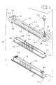
- Figure 1 depicts an exploded perspective view of an electrical connector assembly 10 in accordance with the present invention.
- Electrical connector assembly 10 is comprised of diecast housing 12, drawn shell 14 and header insert 16.
- Diecast housing 12 may be fabricated of any known, electrically conductive material then plated such as with tin; a magnesium alloy, aluminum alloy or zinc alloy is preferred. Die cast housing 12 is elongate, having upper surface 18, lower surface 20 and flanges 22 at opposite ends thereof. Flanges 22 have mounting apertures 24, which may be threaded, extending from upper surface 18 to lower surface 20 for securing connector assembly 10 to a planar surface such as a panel or printed circuit board. Connector assembly 10 may also be secured by other known means such as posts 28 being soldered in corresponding apertures in a printed circuit board. Mounting feet 26 extend from lower surface 20 to space lower surface 20 a predetermined distance from a printed circuit board on which connector assembly 10 is mounted so that flux may be removed subsequent to soldering.
- Latching members 30 extend from upper surface 18 for securing a mated complementary connector (not shown) to connector assembly 10. Upon mating with a complementary connector, latch means on the complementary connector engage and ramp over tapered surface 32 of latch ear 34 thence snap under and engage latching shoulder 36. Key receiving recess or aperture 38 extends from upper surface 18 and is adapted to receive and retain a key 40.
- latch means secure a mated complementary connector to diecast housing 12 which is mounted directly on the planar surface with any resulting forces on the latch means that are transmitted to latching member 30 not subjecting the contacts 82 to any strain.
- aperture 42 extends through diecast housing 12 from upper surface 18 to lower surface 20.
- Electrically conductive shroud 44 has a similar outer profile to aperture 42 and is received therein in an interference fit to assure electrical conductivity between diecast housing 12 and drawn shell 14.
- the profile of shroud 44 is a subminiature D which provides polarization of connector assembly 10 during mating with a complementary connector.
- Shroud 44 of drawn shell 14 extends forwardly of a substantially rectangular flange 46.
- flange 46 prevents drawn shell 14 from passing through aperture 42 by engaging surface 48 which extends around the periphery of aperture 42. Seating flange 46 against surface 48 assures that shroud 44 protrudes forward of upper surface 18 a predetermined appropriate distance.
- shell-to-shield grounding barbs 60 extend inward from endwalls 54 into cavity 58; shell-to-shield grounding barbs 62 extend inward from sidewalls 56 into cavity 58. Grounding barbs 60 and 62 provide an interference fit with the peripheral edge 50 that assures electrical continuity between diecast housing 12 and drawn shell 14.
- Barbs 60, 62 extend from surface 48 along endwalls 54 and sidewalls 56 protruding into cavity 58 to interfere with peripheral edge 50. Tapered surface 64 provides a tapered lead in for flange 46 during insertion. In a preferred embodiment barbs 60, 62 have the shape of a triangular prism with apex 66 providing interference with peripheral edge 50. Alternatively, barbs 60, 62 could be located on drawn shell 14 and engage diecast housing 12 such as along endwalls 54 or sidewalls 56.
- Barbs 60, 62 may be strategically located to center drawn shell 14 in aperture 42 of diecast housing 12 such as by two barbs on one wall and a centered barb on the opposing wall, or by a pair of opposed barbs.
- Figure 2 shows a pair of opposed barbs 60 on endwalls 54 that center drawn shell 14 laterally in aperture 42 and two pairs of opposed barbs 62 on sidewalls 56 that each center drawn shell 14 vertically in aperture 42.
- diecast housing 12 and drawn shell 14 combination is shown in Figure 6 wherein tapered barbs or protrusions 120 on drawn shell 14 pass through aperture 42 thence snap outwardly to secure drawn shell 14 in diecast housing 12.
- This alternate embodiment necessitates inserting drawn shell 14 into aperture 42 before inserting header insert 16 into drawn shell 14.
- flange member 122 flexes outwardly and housing 16 flexes inwardly to permit header insert 16 to pass beyond barbs or protrusions 124 which secures header insert 16 within drawn shell 14.
- Barbs or protrusions 120, 124 may be stamped or formed in drawn shell 14 during or after the drawing process. Barbs 120 also assist in establishing electrical continuity between diecast housing 12 and drawn shell 14.
- a burr 68 may form as peripheral edge 50 passes over apex 66 of barbs 60, 62.
- a burr relief pocket 70 is formed in surface 48 around the periphery of aperture 42 at least in the region of barbs 60, 62 to receive such a burr 68.
- Header insert 16 is molded of thermoplastic and has an insert portion 71, adapted to be received in shroud 44, extending upwardly from integral peripheral flange 72. Insert portion 71 has a similar outer profile to the inside surface of the aperture in shroud 44 and is received therein. Insert 16 has mating face 74, opposed rear face 76 and a plurality of contact receiving passages 78 extending from mating face 74 such as extending between mating face 74 and rear face 76.
- Contact receiving passages 78 typically have tapered lead-in surfaces 80 in mating face 74 to facilitate mating.
- Contacts 82 which are inserted from rear face 76, are secured in contact receiving passages 78 such as by barbs 84 that plow through the plastic forming sidewalls 86 with the plastic flowing around barbs 84.
- Contacts 82 have a mating portion 88 extending into contact receiving passages 78 where sidewalls 86 may provide an antioverstress function, and a mounting portion 90, typically solder posts 92, that extend beyond rear face 76 for mounting such as in apertures 94 in printed circuit board 96.
- Mounting portions 90 are then soldered to traces on the upper and lower surfaces, 108 and 110 respectively, of printed circuit board 96. As best seen in Figure 4, mounting portion 90 of every other contact 82 may be axially offset from the mating portion 88 of the same contact 82 so as to provide a greater space between adjacent apertures 94 in printed circuit board 96.
- Header insert 16 is inserted through cavity 58, mating face 74 first, to seat within drawn shell 14 with mating face 74 terminating proximate edge 98 of drawn shell 14.
- Flange 72 of header insert 16 engages flange 46 of drawn shell 14 to assure that flange 46 engages diecast housing 12 to provide electrical continuity between diecast housing 12 and drawn shell 14 and secure drawn shell 14 in position by clamping flange 46 between surface 48 of diecast housing 12 and flange 72 of header insert 16.
- Drawn shell 14 may include barb means to engage insert 16 and to secure insert 16 in shell 14.
- the barb means may take the form of a sheared, inwardly deflected tab 112 as shown in section in Figure 4.
- Barbs 60, 62 also provide a centering function and fit with header insert 16 to secure header insert 16 within drawn shell 14 and cavity 58 as sidewall 100 of flange 72 engage barbs 60, 62.
- Header insert 16 is further secured within diecast housing 12 by forming a portion of housing 12 subsequent to inserting header insert 16.
- the lower edge 102 of sidewall 100 is molded at an angle and the lower sidewalls of diecast housing 12 is fabricated with a rib 104. Rib 104 is formed over edge 102 at one or more locations forming diecast retention feature 106 as shown on the left side of Figure 4 prior to being formed and on the right side of Figure 4 subsequent to being formed.
- lower edge 102 is molded at a 45 degree angle thus requiring rib 104 to be formed over only 45 degrees. Ribs 104 when formed over provide a diecast retention feature 106 and are less likely to fail than if formed through a large angle such as 90 degrees.
- Figure 5 shows an alternative embodiment connector assembly 10 in which contacts 82 are formed with a 90 degree bend forming a connector in which the mating face is at a right angle with respect to the mounting face.
- connectors shown in the figures are for "through board” mounting where mounting portion 90 of contacts 82 pass through apertures 94 in printed circuit board 96, the invention is not limited thereto.
- the invention has application to surface mount technology where apertures 94 are eliminated and mounting portions 90 are soldered to traces only on the side of printed circuit board 96 on which connector assembly 10 is mounted.
- Connector assembly 10 thus provides a combination of a drawn shell which is proven for shielding with a diecast housing that can be drilled and tapped thus minimizing hardward and providing a durable latching surface.
Landscapes
- Details Of Connecting Devices For Male And Female Coupling (AREA)
- Connector Housings Or Holding Contact Members (AREA)
- Coupling Device And Connection With Printed Circuit (AREA)
Abstract
Description
- This invention relates to an electrical connector assembly and in particular to an electrical connector assembly having a cast housing and drawn shell to provide shielding and a path to ground for the shielding.
- Prior art subminiature D connectors typically had a drawn shell with an integral groundstrap to provide shielding and a conductive path to ground. The drawn shell surrounded a thermoplastic housing in which contact terminals were secured and provided shielding therefor, as discloses in US-A-4,679,883. In another connector assembly described in GB-A-917995, a plastic connector body having terminal receiving cavities with terminals secured therein is disposed in a shell. A metal commoning spring body having contact fingers aligned with the terminal cavities is also disposed in the shell behind the connector body and the two bodies are locked into the shell by suitable means.
- As electronics have become more densely packed, so too have the interconnections to and between electronic assemblies. A widely accepted spacing of contacts has become 1.27mm (0.50 inch) lateral and 2.54mm (.100 inch) vertical in high density connectors. To assure that high density connectors remain mated, latches on the cable assembly connector grip the housing of a board or panel mounted connector. Since plastic would fail under the gripping action of repeated mating and unmating, high density connectors have incorporated cast metal housings. Providing shielding of terminal contacts in cast housings has thus been complicated.
- In accordance with the present invention, an electrical connector assembly for mounting on a planar surface, includes an electrically conductive housing having an aperture therein, and a thermoplastic insert having terminal receiving passages, with terminals secured therein, and disposed in the aperture in the housing which thereby provides shielding for the terminals, and is characterized in that the housing comprises a diecast housing having an aperture therein and a drawn shell also having an aperture therein and received in the diecast housing aperture and electrically commoned with the diecast housing, said thermoplastic insert is secured in the shell aperture, and said shell substantially covers the sides of the insert, whereby the shell provides shielding for the terminals with the diecast housing electrically commoned with the shell for providing an electrical path to a ground on the planar surface.
- The thermoplastic insert may be secured in the diecast housing by forming a portion of the diecast housing over the aperture therein thus preventing removal of the thermoplastic insert.
- The invention will now be described by way of example with reference to the accompanying drawings, in which:
- FIGURE 1 is an exploded perspective view of a connector assembly in accordance with the present invention;
- FIGURE 2 is a rear view of the diecast housing shown in Figure 1;
- FIGURE 3 is a cross sectional view of the diecast housing shown in Figure 1;
- FIGURE 4 is a cross sectional view of the connector assembly shown in Figure 1;
- FIGURE 5 is an alternative embodiment of the connector assembly showing a right angle connector; and
- FIGURE 6 shows a cross-sectional view of an alternative embodiment of connector assembly.
- Figure 1 depicts an exploded perspective view of an
electrical connector assembly 10 in accordance with the present invention.Electrical connector assembly 10 is comprised ofdiecast housing 12, drawnshell 14 andheader insert 16. - Diecast
housing 12 may be fabricated of any known, electrically conductive material then plated such as with tin; a magnesium alloy, aluminum alloy or zinc alloy is preferred. Diecast housing 12 is elongate, havingupper surface 18,lower surface 20 andflanges 22 at opposite ends thereof.Flanges 22 havemounting apertures 24, which may be threaded, extending fromupper surface 18 tolower surface 20 for securingconnector assembly 10 to a planar surface such as a panel or printed circuit board.Connector assembly 10 may also be secured by other known means such asposts 28 being soldered in corresponding apertures in a printed circuit board. Mountingfeet 26 extend fromlower surface 20 to space lower surface 20 a predetermined distance from a printed circuit board on whichconnector assembly 10 is mounted so that flux may be removed subsequent to soldering. - Latching
members 30 extend fromupper surface 18 for securing a mated complementary connector (not shown) toconnector assembly 10. Upon mating with a complementary connector, latch means on the complementary connector engage and ramp overtapered surface 32 oflatch ear 34 thence snap under and engage latchingshoulder 36. Key receiving recess oraperture 38 extends fromupper surface 18 and is adapted to receive and retain akey 40. - In this manner the latch means secure a mated complementary connector to
diecast housing 12 which is mounted directly on the planar surface with any resulting forces on the latch means that are transmitted to latchingmember 30 not subjecting thecontacts 82 to any strain. -
Intermediate flanges 22,aperture 42 extends throughdiecast housing 12 fromupper surface 18 tolower surface 20. Electricallyconductive shroud 44 has a similar outer profile to aperture 42 and is received therein in an interference fit to assure electrical conductivity betweendiecast housing 12 and drawnshell 14. In a preferred embodiment, the profile ofshroud 44 is a subminiature D which provides polarization ofconnector assembly 10 during mating with a complementary connector. -
Shroud 44 of drawnshell 14 extends forwardly of a substantiallyrectangular flange 46. Upon insertion of drawnshell 14 intoaperture 42 from the rear, that is from the side oflower surface 20,flange 46 prevents drawnshell 14 from passing throughaperture 42 byengaging surface 48 which extends around the periphery ofaperture 42.Seating flange 46 againstsurface 48 assures thatshroud 44 protrudes forward of upper surface 18 a predetermined appropriate distance. - Also upon insertion of drawn
shell 14 intoaperture 42 theperipheral edge 50 offlange 46 engages shell-to-shield grounding barbs on theinterior endwalls 54 andsidewalls 56 ofcavity 58. As best seen in Figures 2, 3 and 4, shell-to-shield grounding barbs 60 extend inward fromendwalls 54 intocavity 58; shell-to-shield grounding barbs 62 extend inward fromsidewalls 56 intocavity 58.Grounding barbs peripheral edge 50 that assures electrical continuity betweendiecast housing 12 and drawnshell 14. -
Barbs surface 48 alongendwalls 54 andsidewalls 56 protruding intocavity 58 to interfere withperipheral edge 50. Taperedsurface 64 provides a tapered lead in forflange 46 during insertion. In a preferredembodiment barbs apex 66 providing interference withperipheral edge 50. Alternatively,barbs shell 14 and engagediecast housing 12 such as alongendwalls 54 orsidewalls 56. -
Barbs shell 14 inaperture 42 ofdiecast housing 12 such as by two barbs on one wall and a centered barb on the opposing wall, or by a pair of opposed barbs. Figure 2 shows a pair ofopposed barbs 60 onendwalls 54 that center drawnshell 14 laterally inaperture 42 and two pairs ofopposed barbs 62 onsidewalls 56 that each center drawnshell 14 vertically inaperture 42. - An alternative embodiment
diecast housing 12 and drawnshell 14 combination is shown in Figure 6 wherein tapered barbs orprotrusions 120 on drawnshell 14 pass throughaperture 42 thence snap outwardly to secure drawnshell 14 indiecast housing 12. This alternate embodiment necessitates inserting drawnshell 14 intoaperture 42 before inserting header insert 16 into drawnshell 14. Upon inserting header insert into drawnshell 14,flange member 122 flexes outwardly and housing 16 flexes inwardly to permit header insert 16 to pass beyond barbs orprotrusions 124 which secures header insert 16 within drawnshell 14. Barbs orprotrusions shell 14 during or after the drawing process.Barbs 120 also assist in establishing electrical continuity betweendiecast housing 12 and drawnshell 14. - As drawn
shell 14 is received inaperture 42, a burr 68 may form asperipheral edge 50 passes overapex 66 ofbarbs flange 46seats engaging surface 48, aburr relief pocket 70 is formed insurface 48 around the periphery ofaperture 42 at least in the region ofbarbs -
Header insert 16 is molded of thermoplastic and has aninsert portion 71, adapted to be received inshroud 44, extending upwardly from integralperipheral flange 72. Insertportion 71 has a similar outer profile to the inside surface of the aperture inshroud 44 and is received therein.Insert 16 hasmating face 74, opposedrear face 76 and a plurality ofcontact receiving passages 78 extending frommating face 74 such as extending betweenmating face 74 andrear face 76. - Contact receiving
passages 78 typically have tapered lead-insurfaces 80 inmating face 74 to facilitate mating.Contacts 82, which are inserted fromrear face 76, are secured incontact receiving passages 78 such as bybarbs 84 that plow through theplastic forming sidewalls 86 with the plastic flowing aroundbarbs 84.Contacts 82 have amating portion 88 extending intocontact receiving passages 78 wheresidewalls 86 may provide an antioverstress function, and amounting portion 90, typically solderposts 92, that extend beyondrear face 76 for mounting such as inapertures 94 in printedcircuit board 96. Mountingportions 90 are then soldered to traces on the upper and lower surfaces, 108 and 110 respectively, of printedcircuit board 96. As best seen in Figure 4, mountingportion 90 of everyother contact 82 may be axially offset from themating portion 88 of thesame contact 82 so as to provide a greater space betweenadjacent apertures 94 in printedcircuit board 96. -
Header insert 16 is inserted throughcavity 58,mating face 74 first, to seat within drawnshell 14 withmating face 74 terminatingproximate edge 98 of drawnshell 14.Flange 72 of header insert 16 engagesflange 46 of drawnshell 14 to assure thatflange 46 engagesdiecast housing 12 to provide electrical continuity betweendiecast housing 12 and drawnshell 14 and secure drawnshell 14 in position by clampingflange 46 betweensurface 48 ofdiecast housing 12 andflange 72 ofheader insert 16.Drawn shell 14 may include barb means to engage insert 16 and to secureinsert 16 inshell 14. The barb means may take the form of a sheared, inwardly deflectedtab 112 as shown in section in Figure 4. -
Barbs header insert 16 to secureheader insert 16 within drawnshell 14 andcavity 58 assidewall 100 offlange 72engage barbs Header insert 16 is further secured withindiecast housing 12 by forming a portion ofhousing 12 subsequent to insertingheader insert 16. Thelower edge 102 ofsidewall 100 is molded at an angle and the lower sidewalls ofdiecast housing 12 is fabricated with arib 104.Rib 104 is formed overedge 102 at one or more locations formingdiecast retention feature 106 as shown on the left side of Figure 4 prior to being formed and on the right side of Figure 4 subsequent to being formed. In a preferred embodiment,lower edge 102 is molded at a 45 degree angle thus requiringrib 104 to be formed over only 45 degrees.Ribs 104 when formed over provide adiecast retention feature 106 and are less likely to fail than if formed through a large angle such as 90 degrees. - Figure 5 shows an alternative
embodiment connector assembly 10 in whichcontacts 82 are formed with a 90 degree bend forming a connector in which the mating face is at a right angle with respect to the mounting face. - Although the connectors shown in the figures are for "through board" mounting where mounting
portion 90 ofcontacts 82 pass throughapertures 94 in printedcircuit board 96, the invention is not limited thereto. The invention has application to surface mount technology whereapertures 94 are eliminated and mountingportions 90 are soldered to traces only on the side of printedcircuit board 96 on whichconnector assembly 10 is mounted. -
Connector assembly 10 thus provides a combination of a drawn shell which is proven for shielding with a diecast housing that can be drilled and tapped thus minimizing hardward and providing a durable latching surface.
Claims (10)
Applications Claiming Priority (3)
| Application Number | Priority Date | Filing Date | Title |
|---|---|---|---|
| US07/090,563 US4808125A (en) | 1987-08-31 | 1987-08-31 | Connector assembly with diecast housing and drawn shell |
| US90563 | 1987-08-31 | ||
| PCT/US1988/002614 WO1989002170A1 (en) | 1987-08-31 | 1988-08-01 | Connector assembly with diecast housing and drawn shell |
Publications (3)
| Publication Number | Publication Date |
|---|---|
| EP0331689A1 EP0331689A1 (en) | 1989-09-13 |
| EP0331689B1 true EP0331689B1 (en) | 1994-06-01 |
| EP0331689B2 EP0331689B2 (en) | 1998-03-25 |
Family
ID=22223334
Family Applications (1)
| Application Number | Title | Priority Date | Filing Date |
|---|---|---|---|
| EP88906794A Expired - Lifetime EP0331689B2 (en) | 1987-08-31 | 1988-08-01 | Connector assembly with diecast housing and drawn shell |
Country Status (8)
| Country | Link |
|---|---|
| US (1) | US4808125A (en) |
| EP (1) | EP0331689B2 (en) |
| JP (1) | JPH02501174A (en) |
| KR (1) | KR950012470B1 (en) |
| AT (1) | ATE106618T1 (en) |
| CA (1) | CA1291232C (en) |
| DE (1) | DE3889899T3 (en) |
| WO (1) | WO1989002170A1 (en) |
Families Citing this family (31)
| Publication number | Priority date | Publication date | Assignee | Title |
|---|---|---|---|---|
| US5645717A (en) * | 1989-01-13 | 1997-07-08 | Bio-Rad Laboratories, Inc. | Hydrophobic polymers from water-soluble monomers and their use as chromatography media |
| CA2015898C (en) * | 1989-05-31 | 1996-04-23 | Wayne Samuel Davis | High density ribbon cable connector |
| US4902242A (en) * | 1989-05-31 | 1990-02-20 | Amp Incorporated | Panel mount, cable terminable connector with die cast housing and drawn shell |
| US4960391A (en) * | 1989-06-16 | 1990-10-02 | Amp Incorporated | Hermetically sealed electrical bulkhead connector |
| US5037331A (en) * | 1989-09-27 | 1991-08-06 | Itt Corporation | Shielded interface connector |
| US5046952A (en) * | 1990-06-08 | 1991-09-10 | Amp Incorporated | Right angle connector for mounting to printed circuit board |
| US5055070A (en) * | 1990-08-29 | 1991-10-08 | Labinal Components And Systems, Inc. | Overmolded shielded connector |
| US5064391A (en) * | 1990-09-27 | 1991-11-12 | Amp Incorporated | Asymmetrical high density contact retention |
| US5108317A (en) * | 1991-03-21 | 1992-04-28 | Amp Incorporated | Sealed metal shell connector and method of molding a plastic insert within a metal shell |
| US5147220A (en) * | 1991-05-30 | 1992-09-15 | Lybrand Brent B | Board mounted shielded electrical connector |
| JPH0523453U (en) * | 1991-09-05 | 1993-03-26 | ヒロセ電機株式会社 | Electrical connector structure |
| US5174789A (en) * | 1992-01-21 | 1992-12-29 | Foxconn International, Inc. | Electrical connector with enhanced coupling |
| US5190483A (en) * | 1992-02-14 | 1993-03-02 | Amp Incorporated | Contact retention |
| FR2688634B1 (en) * | 1992-03-10 | 1994-06-03 | Souriau & Cie | POLYGONAL TYPE CONNECTOR, PARTICULARLY RECTANGULAR WITH INSULATING CENTRAL BODY. |
| US5161999A (en) * | 1992-03-18 | 1992-11-10 | Amp Incorporated | Surface mount electrical cohnnector and shield therefor |
| US5167531A (en) * | 1992-03-18 | 1992-12-01 | Amp Incorporated | Stacked electrical connector with diecast housing and drawn shells |
| US5171167A (en) * | 1992-04-09 | 1992-12-15 | Itt Corporation | Connector with resilient intershell connection |
| JP2540705B2 (en) * | 1992-12-01 | 1996-10-09 | 山一電機株式会社 | Shield connector assembly |
| US5344342A (en) * | 1993-01-07 | 1994-09-06 | Amphenol Corporation | Filtered VGA connector |
| US5267876A (en) * | 1993-06-16 | 1993-12-07 | The Whitaker Corporation | Board saving stacked electrical connector assembly |
| US5632649A (en) | 1994-12-22 | 1997-05-27 | The Whitaker Corporation | Hold-down device for a board mount connector |
| US5882214A (en) * | 1996-06-28 | 1999-03-16 | The Whitaker Corporation | Electrical connector with contact assembly |
| US5935429A (en) * | 1997-01-03 | 1999-08-10 | Bio-Rad Laboratories, Inc. | Chromatography columns with continuous beds formed in situ from aqueous solutions |
| US5752854A (en) * | 1997-02-18 | 1998-05-19 | The Whitaker Corporation | Panel mount structure |
| US6139373A (en) * | 1997-04-08 | 2000-10-31 | Thomas & Betts International, Inc. | Multi-pin electrical connectors |
| JP3882958B2 (en) * | 1997-06-30 | 2007-02-21 | タイコエレクトロニクスアンプ株式会社 | Movable connector |
| US6135797A (en) * | 1998-08-13 | 2000-10-24 | The Whitaker Corporation | Electrical connector with floating housing |
| US6659796B1 (en) | 2002-06-21 | 2003-12-09 | Molex Incorporated | Multi-function mounting/latch component for electrical connectors |
| US20040238195A1 (en) * | 2003-05-28 | 2004-12-02 | Craig Thompson | Self-mounting EMI shielding gasket for metal shell electronic apparatus connectors |
| US9742081B1 (en) * | 2016-05-24 | 2017-08-22 | Te Connectivity Corporation | Press-fit circuit board connector |
| CN207651722U (en) * | 2017-11-17 | 2018-07-24 | 连展科技电子(昆山)有限公司 | Electric coupler component |
Family Cites Families (9)
| Publication number | Priority date | Publication date | Assignee | Title |
|---|---|---|---|---|
| US32502A (en) * | 1861-06-11 | Combined thresher and separator | ||
| US3128138A (en) * | 1960-03-23 | 1964-04-07 | Rocco J Noschese | Connector |
| GB2098412B (en) * | 1981-05-11 | 1984-08-01 | Trw Carr Ltd | Shielded electrical connectors |
| JPS59123837A (en) * | 1982-12-29 | 1984-07-17 | Fuji Photo Film Co Ltd | Thermodevelopable color photosensitive material |
| US4512618A (en) * | 1983-03-10 | 1985-04-23 | Amp Incorporated | Grounding mating hardware |
| USRE32502E (en) | 1983-03-10 | 1987-09-15 | Amp Incorporated | Grounding mating hardware |
| US4506937A (en) * | 1983-05-02 | 1985-03-26 | Amp Incorporated | Latching-grounding blocks |
| US4601527A (en) * | 1985-01-18 | 1986-07-22 | E. I. Du Pont De Nemours And Company | Shielded header and cable assembly |
| US4701139A (en) * | 1986-04-25 | 1987-10-20 | Amp Incorporated | Shielded cable assembly |
-
1987
- 1987-08-31 US US07/090,563 patent/US4808125A/en not_active Expired - Lifetime
-
1988
- 1988-08-01 EP EP88906794A patent/EP0331689B2/en not_active Expired - Lifetime
- 1988-08-01 AT AT88906794T patent/ATE106618T1/en not_active IP Right Cessation
- 1988-08-01 WO PCT/US1988/002614 patent/WO1989002170A1/en not_active Ceased
- 1988-08-01 DE DE3889899T patent/DE3889899T3/en not_active Expired - Fee Related
- 1988-08-01 JP JP63506870A patent/JPH02501174A/en active Granted
- 1988-08-01 KR KR1019890700742A patent/KR950012470B1/en not_active Expired - Fee Related
- 1988-08-30 CA CA000576046A patent/CA1291232C/en not_active Expired - Lifetime
Also Published As
| Publication number | Publication date |
|---|---|
| DE3889899T2 (en) | 1995-01-05 |
| KR890702293A (en) | 1989-12-23 |
| JPH0468752B2 (en) | 1992-11-04 |
| US4808125A (en) | 1989-02-28 |
| ATE106618T1 (en) | 1994-06-15 |
| EP0331689B2 (en) | 1998-03-25 |
| CA1291232C (en) | 1991-10-22 |
| WO1989002170A1 (en) | 1989-03-09 |
| DE3889899T3 (en) | 1998-10-15 |
| DE3889899D1 (en) | 1994-07-07 |
| KR950012470B1 (en) | 1995-10-18 |
| EP0331689A1 (en) | 1989-09-13 |
| JPH02501174A (en) | 1990-04-19 |
Similar Documents
| Publication | Publication Date | Title |
|---|---|---|
| EP0331689B2 (en) | Connector assembly with diecast housing and drawn shell | |
| US4963098A (en) | Blind mate shielded input/output connector assembly | |
| US5417590A (en) | Plug and socket electrical connector system | |
| US7037135B2 (en) | Double shielded electrical connector | |
| US5085590A (en) | Shielded stackable connector assembly | |
| JP3104173B2 (en) | Shield connector device | |
| US20150072562A1 (en) | Flippable electrical connector | |
| US4902242A (en) | Panel mount, cable terminable connector with die cast housing and drawn shell | |
| EP0624928B1 (en) | Shielded electrical connector assembly | |
| US6343951B1 (en) | Electrical connector | |
| US6814612B1 (en) | Shielded electrical connector | |
| US7134900B2 (en) | Electrical connector assembly with multi-function latching member | |
| US6749463B1 (en) | Shielded board mounted electrical connector | |
| EP0753213A1 (en) | Shielded electrical connector assembly with shielding back shell | |
| US5611711A (en) | Electrical connector assembly | |
| US6155878A (en) | Electrical connector with separate shield and grounding member | |
| US20040266266A1 (en) | Cable end connector assembly with a shield device | |
| US6893272B2 (en) | Electrical connector assembly having improved grounding means | |
| EP0330497A1 (en) | Blind mate shielded input/output connector assembly | |
| US6293825B1 (en) | Electrical connector | |
| EP0507166B1 (en) | Grounding electrical connector | |
| US5174771A (en) | Electrical connector having externally mounted ground plates | |
| US20040224567A1 (en) | Electrical connector with improved locking device | |
| US6568958B2 (en) | Electrical connector having improved performance regarding resistance to high voltage penetration | |
| EP0510264B1 (en) | Coaxial cable connector system |
Legal Events
| Date | Code | Title | Description |
|---|---|---|---|
| PUAI | Public reference made under article 153(3) epc to a published international application that has entered the european phase |
Free format text: ORIGINAL CODE: 0009012 |
|
| AK | Designated contracting states |
Kind code of ref document: A1 Designated state(s): AT BE CH DE FR GB IT LI LU NL SE |
|
| 17P | Request for examination filed |
Effective date: 19890905 |
|
| RAP1 | Party data changed (applicant data changed or rights of an application transferred) |
Owner name: AMP INCORPORATED |
|
| 17Q | First examination report despatched |
Effective date: 19920707 |
|
| RAP1 | Party data changed (applicant data changed or rights of an application transferred) |
Owner name: THE WHITAKER CORPORATION |
|
| GRAA | (expected) grant |
Free format text: ORIGINAL CODE: 0009210 |
|
| AK | Designated contracting states |
Kind code of ref document: B1 Designated state(s): AT BE CH DE FR GB IT LI LU NL SE |
|
| REF | Corresponds to: |
Ref document number: 106618 Country of ref document: AT Date of ref document: 19940615 Kind code of ref document: T |
|
| RBV | Designated contracting states (corrected) |
Designated state(s): DE FR GB IT NL |
|
| REF | Corresponds to: |
Ref document number: 3889899 Country of ref document: DE Date of ref document: 19940707 |
|
| ITF | It: translation for a ep patent filed | ||
| ET | Fr: translation filed | ||
| PLBI | Opposition filed |
Free format text: ORIGINAL CODE: 0009260 |
|
| 26 | Opposition filed |
Opponent name: FRAMATOME CONNECTORS INTERNATIONAL Effective date: 19950228 |
|
| NLR1 | Nl: opposition has been filed with the epo |
Opponent name: FRAMATOME CONNECTORS INTERNATIONAL |
|
| PLAW | Interlocutory decision in opposition |
Free format text: ORIGINAL CODE: EPIDOS IDOP |
|
| PLAW | Interlocutory decision in opposition |
Free format text: ORIGINAL CODE: EPIDOS IDOP |
|
| PUAH | Patent maintained in amended form |
Free format text: ORIGINAL CODE: 0009272 |
|
| STAA | Information on the status of an ep patent application or granted ep patent |
Free format text: STATUS: PATENT MAINTAINED AS AMENDED |
|
| 27A | Patent maintained in amended form |
Effective date: 19980325 |
|
| AK | Designated contracting states |
Kind code of ref document: B2 Designated state(s): DE FR GB IT NL |
|
| ITF | It: translation for a ep patent filed | ||
| NLR2 | Nl: decision of opposition | ||
| NLR3 | Nl: receipt of modified translations in the netherlands language after an opposition procedure | ||
| ET3 | Fr: translation filed ** decision concerning opposition | ||
| REG | Reference to a national code |
Ref country code: GB Ref legal event code: IF02 |
|
| PGFP | Annual fee paid to national office [announced via postgrant information from national office to epo] |
Ref country code: NL Payment date: 20050716 Year of fee payment: 18 |
|
| PGFP | Annual fee paid to national office [announced via postgrant information from national office to epo] |
Ref country code: GB Payment date: 20050727 Year of fee payment: 18 |
|
| PGFP | Annual fee paid to national office [announced via postgrant information from national office to epo] |
Ref country code: FR Payment date: 20050817 Year of fee payment: 18 |
|
| PGFP | Annual fee paid to national office [announced via postgrant information from national office to epo] |
Ref country code: DE Payment date: 20050930 Year of fee payment: 18 |
|
| PGFP | Annual fee paid to national office [announced via postgrant information from national office to epo] |
Ref country code: IT Payment date: 20060831 Year of fee payment: 19 |
|
| PG25 | Lapsed in a contracting state [announced via postgrant information from national office to epo] |
Ref country code: DE Free format text: LAPSE BECAUSE OF NON-PAYMENT OF DUE FEES Effective date: 20070301 Ref country code: NL Free format text: LAPSE BECAUSE OF NON-PAYMENT OF DUE FEES Effective date: 20070301 |
|
| GBPC | Gb: european patent ceased through non-payment of renewal fee |
Effective date: 20060801 |
|
| NLV4 | Nl: lapsed or anulled due to non-payment of the annual fee |
Effective date: 20070301 |
|
| REG | Reference to a national code |
Ref country code: FR Ref legal event code: ST Effective date: 20070430 |
|
| PG25 | Lapsed in a contracting state [announced via postgrant information from national office to epo] |
Ref country code: GB Free format text: LAPSE BECAUSE OF NON-PAYMENT OF DUE FEES Effective date: 20060801 |
|
| PG25 | Lapsed in a contracting state [announced via postgrant information from national office to epo] |
Ref country code: FR Free format text: LAPSE BECAUSE OF NON-PAYMENT OF DUE FEES Effective date: 20060831 |
|
| PG25 | Lapsed in a contracting state [announced via postgrant information from national office to epo] |
Ref country code: IT Free format text: LAPSE BECAUSE OF NON-PAYMENT OF DUE FEES Effective date: 20070801 |