EP0330425A2 - Symmetric multi-processing control arrangement - Google Patents
Symmetric multi-processing control arrangement Download PDFInfo
- Publication number
- EP0330425A2 EP0330425A2 EP89301666A EP89301666A EP0330425A2 EP 0330425 A2 EP0330425 A2 EP 0330425A2 EP 89301666 A EP89301666 A EP 89301666A EP 89301666 A EP89301666 A EP 89301666A EP 0330425 A2 EP0330425 A2 EP 0330425A2
- Authority
- EP
- European Patent Office
- Prior art keywords
- processor
- entry
- priority level
- memory
- synchronization
- Prior art date
- Legal status (The legal status is an assumption and is not a legal conclusion. Google has not performed a legal analysis and makes no representation as to the accuracy of the status listed.)
- Granted
Links
Images
Classifications
-
- G—PHYSICS
- G06—COMPUTING; CALCULATING OR COUNTING
- G06F—ELECTRIC DIGITAL DATA PROCESSING
- G06F9/00—Arrangements for program control, e.g. control units
- G06F9/06—Arrangements for program control, e.g. control units using stored programs, i.e. using an internal store of processing equipment to receive or retain programs
- G06F9/46—Multiprogramming arrangements
- G06F9/52—Program synchronisation; Mutual exclusion, e.g. by means of semaphores
Definitions
- the invention relates generally to the field of digital data processing systems, and more specifically to mechanisms for controlling access to code and data which may be shared in a digitial data processing system including multiple processors.
- a digital data processing system includes three basic elements, namely, a processor element, a memory element and an input/output element.
- the memory element stores information in addressable storage locations. This information includes data and instructions for processing the data.
- the processor element fetches information from the memory element, interprets the information as either an instuction or data, processes the data in accordance with the instructions, and returns the processed data to the memory element for storage therein.
- the input/output element under control of the processor element, also communicates with the memory element to transfer information, including instructions and data to be processed, to the memory, and to obtain processed data from the memory.
- an input/output element includes a number of diverse types of units, including video display terminals, printers, interfaces to the public telecommunications network, and secondary storage subsystems, including disk and tape storage devices.
- a video display terminal permits a user to run programs and input data and view processed data.
- a printer permits a user to obtain processed data on paper.
- An interface to the public telecommunications network permits transfer of information over the public telecommunications network.
- multi processing systems which include multiple processors.
- Such multi processing systems are generally organized along two paradigms for controlling operations within a system.
- one paradigm called "master-slave"
- one processor operates as a master processor, essentially assigning jobs to the other processors, which operate as slave processors.
- the master processor may also perform similar jobs as a slave processor while it is not performing its assignment functions.
- Control is simplified in systems designed along the master-slave paradigm since a single processor, namely, the master processor, is responsible for assigning the jobs.
- the master processor if the master processor malfunctions, the entire system may be inoperative.
- the master processor may become overloaded, which will slow down assignments of jobs to the slave processors.
- jobs are identified in a list stored in memory which may be accessed by any processor in the system. When a processor becomes available, it may retrieve an item from the job list for processing. Loading items onto the job list is, itself a job which can be performed by any of the processors, thus control of the job list is also decentralized among all of the processors. Since all of the processors can perform these control functions, if any of them malfunctions the systems can remain operative, although at a reduced processing speed.
- decentralized systems can also have problems if the operating system, the program which controls the processors and job scheduling, does not provide good coordination and communication among the processors. It is necessary, in a decentralized system, to ensure that, for example, two processors do not attempt to execute the same critical section or region at the smae time.
- a critical region is a portion of a program in which memory shared among the processors is accessed [see, for example, A Tanenbaum, Operating Systems: Design and Implementation, (Prentice-Hall, 1987), at page 53].
- flags are used to provide synchronization of access to critical regions of programs and of shared data structures processed thereby.
- the flags which comprise storage locations in memory which are shared among processors in the system, can be used to indicate the status of a critical region that is, whether or not a critical region, is being executed.
- a processor wishes to execute a critical region, it can set the flag associated with the critical region to inform other processors that the critical region is being executed.
- another processor wishes to execute the same critical region, it determines the condition of the flag, and, if the flag does not indicate that the critical region is being executed by another processor, may itself execute the critical region, first conditioning the flag to indicate that the critical region is being executed.
- the processor wishing to execute the critical region delays, continuing to test the flag until it is changed to indicate that the critical region is not being executed by another processor.
- a race condition may occur if two processors request the same critical region at the same time. If neither is able to condition to semaphore to indicate that the critical region is being executed before the other tests the semaphore's condition, both may execute the critical region.
- Another problem termed “deadlock” occurs when two processors need to execute the critical region currently being processed by the other. Since neither can release the critical region each is executing, neither can begin executing the other critical region. As a result, both processors are deadlocked.
- a semaphore manages control of the sychronization flags and gives permission to one processor if several request access to the same critical region at the same time.
- a processor finishes execution of a critical region, it informs the semaphore, which is responsible for conditioning the flags.
- a problem arises, however, since, if a processor is denied access to a critical region, it may continually attempt to obtain permission from the semaphore until it gives permission to the processor to execute the critical region. If this occurs with sufficient numbers of the processors in the multiple processor system, the communications system in the digital data processing system may be so overloaded with requests that no other communciation can take place. At this point, the system is effectively unable to perform processing work.
- the invention provides a new and improved mechanism for synchronizing execution of shared critical regions in a digital data processing system.
- the digital data processing system includes a plurality of processors, each including a central processor unit for processing programs at predetermined synchronization priority levels and a cache memory.
- a memory shared by all of the processors includes a synchronization level table which identifies a processor operating at the various synchronization priority levels.
- a common bus interconnects the processors and the memory.
- the processor If the synchronization priority level is not accessible, the processor continually monitors the entry in the synchronization level table to determine when it is accessible. In that operation, the processor monitors its cache, which contains a copy of the table entry associated with the synchronization priority level, rather than the entry in the memory, thereby minimizing the number of transfers required with the memory over the common bus. When the synchronization priority level becomes accessible, the cache copy is invalidated so that the processor then has to use the table in the memory.
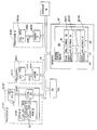
- a digital data processing system constructed in accordance with the invention includes one or more processors 10(O) through 10(N) (generally identified by reference numeral 10) each including a central processing unit 11(O) through 11(N) (generally identified by reference numeral 11) and a cache 12(O) through 12(N) (generally identified by reference numeral 12) interconnected by a bus 13(O) through 13(N) (generally identified by reference numeral 13).
- Each of the caches 23 in each of the processors 10 is also connected to a bus 14.
- the bus 14 permits the processors 10 to communicate with each other and with a console 16, a memory 17, and one or more input/output units 20.
- Each central processor unit 11 executes instructions that are stored in addressable storage locations in the memory 17.
- the instructions identify operations that are to be performed on operands, which are also stored in addressable locations in the memory 17.
- the instructions and operands are fetched by the central processor units 11 as they are needed, and processed data are returned for storage in the memory 17.
- the central processor units 11 also transmit control information to the input/output units 20, enabling them to perform selected operations, such as transmitting data to or retrieving data from the memory 17.
- Such data may include instructions or operands which may be transmitted to the memory 17 or processed data which is retrieved from the memeory 17 for storage or display.
- An operators console 16 serves as the operator's interface. It allows the operator to examine and deposit data, halt the operation of the central processor unit 11 or step the central processor unit 11 through a sequence of instructions and determine the responses of the central processor unit 11 in response thereto. It also enables an operator to initialize the system through a boot strap procedure, and perform various diagnostic tests on the entire data processing system. As is typical, the console 16 may be connected directly to each processor 10, or to selected processors, over communications mechanisms other than bus 14.
- the memory 17 includes a memory controller, which is connected directly to the bus 14 and to a plurality of arrays.
- the arrays contain a plurality of addressable storage location in which information is stored.
- the memory controller receives transfer requests from the central processor units 11 or an input/output unit 20 over the bus 14.
- transfer requests may be transmitted over bus 14, which fall into two general categories. In one category. information is written into, or stored in, a storage location, and in the other category, information is retrieved, or read, from a storage location, the storage location being identified by an address transmitted with the transfer request.
- the digital data processing system depicted in Fig. 1 may include several types of input/output units 20, including disk and tape secondary storage units, teletypewriters, video display terminals, line printers, telephone and computer network interface units, and the like.
- the disk secondary storage units may provide mass storage of data which, under control of central processor unit 11, is tranferred to and from the memory
- cache 12(O) includes a cache memory 21 including a plurality of cache entries generally indentified by reference numeral 22, one of which is depicted in the Fig., and a cache control circuit 23.
- Each cache entry 22 maintains a copy of information from a selected number of locations in memory 17.
- the cache control circuit 23 maintains the information in the entries of cache memory 21 from locations in memory 17 from which the processor 10, and specifically central processor unit 11, has recently retrieved information.
- Each entry 22 in the cache memory 21 includes several fields, including a validity flag 24, an address field 25 and one or more data fields 26.
- the contents of the address field 25 identifies the location of memory 17 from which the data in the data fields 26 was copied.
- the validity flag 24 indicates whether the entry 22 contains valid data. That is, if the validity flag 24 is set, the data fields 26 in the entry 22 contain a valid or correct copy of the data in the location identified by the address in the address field 25. On the other hand, if the validity flag 24 is not set, the data fields 25 in the entry 22 do not contain a correct copy of the data in the location identified by the address in the address field, as described below.
- the central processor unit 11 When the central processor unit 11 needs to retrieve information from a selected location in the memory 17, it transmits a retrieval request over bus 13 to the cache 12, and specifically the cache control circuit 23. In initiating the retrieval operation, the central processor unit 11 identifies by address the location in memory 17 which contains the required information. The cache control circuit 23 searches through the contents of the address fields 25 in the entries 22 in the cache memory 21 to determine if one of the address fields contains the address received from the central processor unit 11. If one does, and if the validity flag 24 of the entry 22 is set, the cache control circuit 23 retrieves the contents of a data field 26 for transmission over 13 to the central processor unit 11.
- the cache control circuit 23 determines (1) that the contents of the address field 25 of an entry 22 corresponds to the address received from central processor unit 11 but that the validity flag 24 of that entry is reset, or (2) that none of the contents of the address fields 25 of entries 22 correspond to the address received from central processor unit 11, the cache control circuit 23 initiates a retrieval operation over bus 14 to retrieve the contents of the identified location. In this operation, the cache control circuit 23 identifies the location identified by the central processor unit 11. Typically, the cache control circuit 23 will contemporaneously initiate retrieval of information from proximate locations in memory 17.
- the memory 17 returns the contents of the identified locations over bus 14, and the cache control circuit 23 then transmits the information from the requested locations in memory 17 to the central processor unit 11 over bus 13 and stores the information in the data fields 26 in the cache memory 21, with the contents of each location retrieved from memory 17 being stored in a data field 26 in the entry 22 in cache memory 21, with the validity flag 24 set in the entry 22.
- the cache control circuit determines that an entry 22 in cache memory 21 does contain a copy of the contents of the location in memory 17 requested by the central processor unit 11, it retrieves the data from a data field 26 and transfers it to the central processor unit 11 over the bus 13. In this situation, the cache 12 does not have to perform a transfer over bus 14 to supply the central processor unit 11 with the requested information, which can reduce transfers over bus 14.
- a central processor unit 11 When a central processor unit 11 initiates a write operation to transfer information for storage in an identified location in memory 17, it transmits the information and the identification of the location in which the information is to be stored over bus 13.
- the cache 12 is a write through cache
- the cache control circuit 23 when the central processor unit 11 initiates a transfer to store information in a location in memory 17, the cache control circuit 23 initiates a tranfer over bus 15 to enable the information to be stored in the identified location in memory 17.
- the cache contol circuit determines whether the contents of the address field 25 in an entry 22 in the cache memory correspond to the address received from the central processor unit 11.
- the cache control circuit 23 may either store the information in a data field 26 in the entry, over-writing the information with the new information, or reset the valid flag 24 of the entry 22 so that the cache control circuit 23 will retrieve the information from the memory 17 when it next receives a retrieval request from the central processor unit 11 identifying the location in memory 17.
- the cache control circuit 23 also monitors the write operations initiated by other processors 10 over bus 14. When the cache control circuit receives a write operation over bus 14 which identifies a location in memory 17 whose address corresponds to the address contained in the address field 25 of an entry 22 in cache memory 21, the cache control circuit 23 resets the valid flag 24 of the entry 22. When the central processor unit 11 later requests retrieval identifying the location, the cache control circuit 23 then initiates the retrieval operation from memory 17 over bus 14.
- the memory 17 includes a plurality of addressable storage locations, some of which comprise a system status block 30 in which is stored status information used by all of the processors 10.
- the system status block 30 includes a synchronization table 31 which, in turn, includes a plurality of entries 32(1) through 32(M) (generally identified by reference numeral 32). Each entry 32 includes two fields, including a flag field 36 and a processor identification field 34.
- the processor 10 in the digital data processing system depicted in the Fig. operate in one of a plurality of synchronization priority levels.
- the digital data processing system is a VAX system sold by, and as described in the VAX-11 Architecture Reference Manual published by, Digital Equipment Corporation, the assignee of the present application
- the synchronization priority levels are related to interrupt priority levels.
- Each interrupt priority level is associated with several synchronization priority levels, with each synchronization priority level controlling access to selected data structures, and thus critical regions which use the data structures, that form part of programs which are processed at that interrupt priority level. It will be appreciated, therefore, that the synchronization priority level synchronizes access to data structures as well as synchronizing processing of critical regions of programs.
- each processor 10 is maintained at a synchronization priority level.
- Each critical region in a program which may be processed by the processors 10 in the system is assigned a synchronization priority level, and to process any program at a priority level, the processor must adjust 7ts synchronization priority level prior to processing the critical region. Since all of the programs in the system, and thus all of the program's critical regions, can be processed by any of the processors 10, to synchronize processing within the system, only one processor 10 can be operating at each synchronization priority level at one time.
- the system synchronization level table 31 includes one entry 32 for each of the synchronization priority levels in the digital data processing system, with the order of the entry 32 in the table corresponding to the entry's associated synchronization priority level.
- the processor identification field 34 in each entry 32 identifies the processor 10, if any which is operating at the synchronization priority level identified by the entry's synchronization priority level. If no processor 10 is operating at the synchronization priority level, the processor identification field 34 is empty.
- the flag 36 in each entry 32 indicates whether a processor is operating at the entry's associated synchronization priority level. If the flag 36 in an entry 32 is clear, no processor is operating at that synchronization priority level. On the other hand, if the flag 36 in an entry 32 is set, the processor 10 which is identified in processor identification field 34 of the entry 32 is operating at the entry's synchronization priority level.
- a processor 10 When a processor 10, and specifically a central processor unit 11, needs to execute a critical region of a program which requires a specific synchronization priority level, the processor 10 executes a conventional semaphore program which controls the synchronization level table 31 and, thus, access to the various synchronization priority levels. In that operation, the processor 10, under control of the semaphore program, retrieves the contents of and interrogates the entry 32 in the synchronization level table 31 associated with that synchronization priority level.
- the semaphore program loads the identification of the processor 10 into the processor identification field 24 in that entry 32 to indicate that the synchronization priority level associated with the entry 32 is occupied by the processor 10 and sets the flag 36 in the entry 32 to indicate that the synchronization priority level is occupied.
- the processor 10 then processes the critical region and, when it is finished, clears the flag 36 of the entry 32 to indicate that the synchronization priority level is available.
- the processors each process the semaphore program to jointly determine which processor 10 may use the synchronization priority level.
- the semaphore program executing on the winning processor 10 sets the flag 36 and loads its identification into the processor identification field 34 of the entry 32 in the synchronization level table 31 associated with the synchronization priority level.
- the winning processor 10 then processes the critical region and, when it is finished, clears the flag 36 of the entry 32 to indicate that the synchronization priority level is available.
- the losing processor or processors 10 While the winning processor 10 is executing a critical region at the synchronization priority level, the losing processor or processors 10 continue their attempts to obtain access to the synchronization priority level. In that operation, they continually monitor the condition of the entry 32, and specifically the entry's flag 36, in the synchronization level table 31 to determine when the winning processor 10 clears the flag 36 to indicate that the synchronization priority level associated with the entry 32 is available. To do this, the central processor unit 11 repeatedly initiates retrieval operations over its bus 13 to retrieve the contents of the storage location in memory 17 in which the entry 32 is stored.
- the cache control circuit 23 retrieves the contents of the cache entry 22 which stores the copy of the entry 32 from the synchronization level table 31, until the processor 10 that won the use of the synchronization priority level performs a write operation over bus 14 to clear the flag 36 in the entry 32 associated with the synchronization priority level.
- the cache control circuits 23 in the other processors invalidate their cache entries 22 for that location in memory 17.
- the cache control circuits 23 will perform the retrieval operation with memory 17, rather than their caches 21, to thereby retrieve the updated flag 36 from the system status block 30 in memory 17.
- the winning processor 10 when it relinquishes the synchronization priority level, performs a write operation to reset the contents of the flag 36 of cache entry 32. Since the cache control circuits 23 monitor write operations over bus 14 to reset the flags 36 of cache entries 22 whose address fields 25 are identified in the write operation, when the winning processor performs the write operation to relinquish the synchronization priority level, the cache control circuits 23 in the losing processors 10 will reset the valid flags 24 of the cache entries 22 whose address fields 25 identify the storage location in memory 17 which contains the entry 32.
- the cache control circuit 23 will initiate an operation over the bus 14 to retrieve the entry from memory 17. Since this occurs only after the winning processor 10 has conditioned the entry 32 to indicate that the synchronization priority level is available, the losing processors 10 will not initiate operations over bus 14 until the synchronization priority level is available.
Abstract
Description
- The invention relates generally to the field of digital data processing systems, and more specifically to mechanisms for controlling access to code and data which may be shared in a digitial data processing system including multiple processors.
- A digital data processing system includes three basic elements, namely, a processor element, a memory element and an input/output element. The memory element stores information in addressable storage locations. This information includes data and instructions for processing the data. The processor element fetches information from the memory element, interprets the information as either an instuction or data, processes the data in accordance with the instructions, and returns the processed data to the memory element for storage therein. The input/output element, under control of the processor element, also communicates with the memory element to transfer information, including instructions and data to be processed, to the memory, and to obtain processed data from the memory.
- Typically, an input/output element includes a number of diverse types of units, including video display terminals, printers, interfaces to the public telecommunications network, and secondary storage subsystems, including disk and tape storage devices. A video display terminal permits a user to run programs and input data and view processed data. A printer permits a user to obtain processed data on paper. An interface to the public telecommunications network permits transfer of information over the public telecommunications network.
- To increase processing speed, digital data processing systems have been developed which include multiple processors. Such multi processing systems are generally organized along two paradigms for controlling operations within a system. In one paradigm, called "master-slave", one processor operates as a master processor, essentially assigning jobs to the other processors, which operate as slave processors. The master processor may also perform similar jobs as a slave processor while it is not performing its assignment functions. Control is simplified in systems designed along the master-slave paradigm since a single processor, namely, the master processor, is responsible for assigning the jobs. However, in such systems, if the master processor malfunctions, the entire system may be inoperative. In addition, under heavy processing loads, the master processor may become overloaded, which will slow down assignments of jobs to the slave processors.
- Problems with systems designed along the master-slave paradigm do not arise in systems designed along the second paradigm, in which assigment of work is handled in a more homogeneous manner. In this paradigm, jobs are identified in a list stored in memory which may be accessed by any processor in the system. When a processor becomes available, it may retrieve an item from the job list for processing. Loading items onto the job list is, itself a job which can be performed by any of the processors, thus control of the job list is also decentralized among all of the processors. Since all of the processors can perform these control functions, if any of them malfunctions the systems can remain operative, although at a reduced processing speed.
- While decentralization of the control functions in a multiple processing system provides some advantages over systems employing master-slave control, decentralized systems can also have problems if the operating system, the program which controls the processors and job scheduling, does not provide good coordination and communication among the processors. It is necessary, in a decentralized system, to ensure that, for example, two processors do not attempt to execute the same critical section or region at the smae time. A critical region is a portion of a program in which memory shared among the processors is accessed [see, for example, A Tanenbaum, Operating Systems: Design and Implementation, (Prentice-Hall, 1987), at page 53]. If two processors attempt to execute a critical region of a program at the same time, they may access data in the same storage location in an overlapping, rather than sequential, manner, which will result in an erroneous result. This problem can occur if the system does not provide good synchronization among critical regions.
- Typically, flags are used to provide synchronization of access to critical regions of programs and of shared data structures processed thereby. The flags, which comprise storage locations in memory which are shared among processors in the system, can be used to indicate the status of a critical region that is, whether or not a critical region, is being executed. When a processor wishes to execute a critical region, it can set the flag associated with the critical region to inform other processors that the critical region is being executed. If another processor wishes to execute the same critical region, it determines the condition of the flag, and, if the flag does not indicate that the critical region is being executed by another processor, may itself execute the critical region, first conditioning the flag to indicate that the critical region is being executed. On the other hand, if the flag does indicate that the critical region is being executed by another processor, the processor wishing to execute the critical region delays, continuing to test the flag until it is changed to indicate that the critical region is not being executed by another processor.
- The use of flags to control access to a shared critical region does create several problems. One problem, termed a "race" condition, may occur if two processors request the same critical region at the same time. If neither is able to condition to semaphore to indicate that the critical region is being executed before the other tests the semaphore's condition, both may execute the critical region. Another problem, termed "deadlock" occurs when two processors need to execute the critical region currently being processed by the other. Since neither can release the critical region each is executing, neither can begin executing the other critical region. As a result, both processors are deadlocked.
- To alleviate race and deadlock problems, more sophisticated control mechanisms, known as semaphores, have been developed. A semaphore manages control of the sychronization flags and gives permission to one processor if several request access to the same critical region at the same time. When a processor finishes execution of a critical region, it informs the semaphore, which is responsible for conditioning the flags. A problem arises, however, since, if a processor is denied access to a critical region, it may continually attempt to obtain permission from the semaphore until it gives permission to the processor to execute the critical region. If this occurs with sufficient numbers of the processors in the multiple processor system, the communications system in the digital data processing system may be so overloaded with requests that no other communciation can take place. At this point, the system is effectively unable to perform processing work.
- The invention provides a new and improved mechanism for synchronizing execution of shared critical regions in a digital data processing system.
- In brief summary, the digital data processing system includes a plurality of processors, each including a central processor unit for processing programs at predetermined synchronization priority levels and a cache memory. A memory shared by all of the processors includes a synchronization level table which identifies a processor operating at the various synchronization priority levels. A common bus interconnects the processors and the memory. When a processor is to execute a critical region, it adjusts its synchronization priority level to a predetermined level. In that operation, the processor accesses the synchronization level table to determine whether the synchronization priority level is accessible and, if so, places an entry in the table to indicate that the synchronization priority level is occupied. If the synchronization priority level is not accessible, the processor continually monitors the entry in the synchronization level table to determine when it is accessible. In that operation, the processor monitors its cache, which contains a copy of the table entry associated with the synchronization priority level, rather than the entry in the memory, thereby minimizing the number of transfers required with the memory over the common bus. When the synchronization priority level becomes accessible, the cache copy is invalidated so that the processor then has to use the table in the memory.
- This invention is pointed out with particularity in the appended claims. The above and further advantages of this invention may be better understood by referring to the following description taken in conjunction with the accompanying drawing, which depicts a block diagram of a digital data processing system constructed in accordance with the invention.
- Referring to Fig. 1, a digital data processing system constructed in accordance with the invention includes one or more processors 10(O) through 10(N) (generally identified by reference numeral 10) each including a central processing unit 11(O) through 11(N) (generally identified by reference numeral 11) and a cache 12(O) through 12(N) (generally identified by reference numeral 12) interconnected by a bus 13(O) through 13(N) (generally identified by reference numeral 13). Each of the
caches 23 in each of theprocessors 10 is also connected to abus 14. Thebus 14 permits theprocessors 10 to communicate with each other and with aconsole 16, a memory 17, and one or more input/output units 20. - Each
central processor unit 11 executes instructions that are stored in addressable storage locations in the memory 17. The instructions identify operations that are to be performed on operands, which are also stored in addressable locations in the memory 17. The instructions and operands are fetched by thecentral processor units 11 as they are needed, and processed data are returned for storage in the memory 17. Thecentral processor units 11 also transmit control information to the input/output units 20, enabling them to perform selected operations, such as transmitting data to or retrieving data from the memory 17. Such data may include instructions or operands which may be transmitted to the memory 17 or processed data which is retrieved from the memeory 17 for storage or display. - An
operators console 16 serves as the operator's interface. It allows the operator to examine and deposit data, halt the operation of thecentral processor unit 11 or step thecentral processor unit 11 through a sequence of instructions and determine the responses of thecentral processor unit 11 in response thereto. It also enables an operator to initialize the system through a boot strap procedure, and perform various diagnostic tests on the entire data processing system. As is typical, theconsole 16 may be connected directly to eachprocessor 10, or to selected processors, over communications mechanisms other thanbus 14. - The memory 17 includes a memory controller, which is connected directly to the
bus 14 and to a plurality of arrays. The arrays contain a plurality of addressable storage location in which information is stored. The memory controller receives transfer requests from thecentral processor units 11 or an input/output unit 20 over thebus 14. Several types of transfer requests may be transmitted overbus 14, which fall into two general categories. In one category. information is written into, or stored in, a storage location, and in the other category, information is retrieved, or read, from a storage location, the storage location being identified by an address transmitted with the transfer request. - The digital data processing system depicted in Fig. 1 may include several types of input/
output units 20, including disk and tape secondary storage units, teletypewriters, video display terminals, line printers, telephone and computer network interface units, and the like. The disk secondary storage units may provide mass storage of data which, under control ofcentral processor unit 11, is tranferred to and from the memory - The
caches 12 used in the system depicted in the Fig. are conventional caches. Since all of thecaches 23 are similar, only cache 12(O) is depicted in detail. As is conventional, cache 12(O) includes acache memory 21 including a plurality of cache entries generally indentified byreference numeral 22, one of which is depicted in the Fig., and acache control circuit 23. Eachcache entry 22 maintains a copy of information from a selected number of locations in memory 17. Thecache control circuit 23 maintains the information in the entries ofcache memory 21 from locations in memory 17 from which theprocessor 10, and specificallycentral processor unit 11, has recently retrieved information. - Each
entry 22 in thecache memory 21 includes several fields, including avalidity flag 24, anaddress field 25 and one or more data fields 26. The contents of theaddress field 25 identifies the location of memory 17 from which the data in the data fields 26 was copied. Thevalidity flag 24 indicates whether theentry 22 contains valid data. That is, if thevalidity flag 24 is set, the data fields 26 in theentry 22 contain a valid or correct copy of the data in the location identified by the address in theaddress field 25. On the other hand, if thevalidity flag 24 is not set, the data fields 25 in theentry 22 do not contain a correct copy of the data in the location identified by the address in the address field, as described below. - When the
central processor unit 11 needs to retrieve information from a selected location in the memory 17, it transmits a retrieval request overbus 13 to thecache 12, and specifically thecache control circuit 23. In initiating the retrieval operation, thecentral processor unit 11 identifies by address the location in memory 17 which contains the required information. Thecache control circuit 23 searches through the contents of the address fields 25 in theentries 22 in thecache memory 21 to determine if one of the address fields contains the address received from thecentral processor unit 11. If one does, and if thevalidity flag 24 of theentry 22 is set, thecache control circuit 23 retrieves the contents of adata field 26 for transmission over 13 to thecentral processor unit 11. - On the other hand, if the
cache control circuit 23 determines (1) that the contents of theaddress field 25 of anentry 22 corresponds to the address received fromcentral processor unit 11 but that thevalidity flag 24 of that entry is reset, or (2) that none of the contents of the address fields 25 ofentries 22 correspond to the address received fromcentral processor unit 11, thecache control circuit 23 initiates a retrieval operation overbus 14 to retrieve the contents of the identified location. In this operation, thecache control circuit 23 identifies the location identified by thecentral processor unit 11. Typically, thecache control circuit 23 will contemporaneously initiate retrieval of information from proximate locations in memory 17. The memory 17 returns the contents of the identified locations overbus 14, and thecache control circuit 23 then transmits the information from the requested locations in memory 17 to thecentral processor unit 11 overbus 13 and stores the information in the data fields 26 in thecache memory 21, with the contents of each location retrieved from memory 17 being stored in adata field 26 in theentry 22 incache memory 21, with thevalidity flag 24 set in theentry 22. - If, on the other hand, the cache control circuit determines that an
entry 22 incache memory 21 does contain a copy of the contents of the location in memory 17 requested by thecentral processor unit 11, it retrieves the data from adata field 26 and transfers it to thecentral processor unit 11 over thebus 13. In this situation, thecache 12 does not have to perform a transfer overbus 14 to supply thecentral processor unit 11 with the requested information, which can reduce transfers overbus 14. - When a
central processor unit 11 initiates a write operation to transfer information for storage in an identified location in memory 17, it transmits the information and the identification of the location in which the information is to be stored overbus 13. In one enbodiment in which thecache 12 is a write through cache, when thecentral processor unit 11 initiates a transfer to store information in a location in memory 17, thecache control circuit 23 initiates a tranfer over bus 15 to enable the information to be stored in the identified location in memory 17. In addition, the cache contol circuit determines whether the contents of theaddress field 25 in anentry 22 in the cache memory correspond to the address received from thecentral processor unit 11. If so, it may either store the information in adata field 26 in the entry, over-writing the information with the new information, or reset thevalid flag 24 of theentry 22 so that thecache control circuit 23 will retrieve the information from the memory 17 when it next receives a retrieval request from thecentral processor unit 11 identifying the location in memory 17. - The
cache control circuit 23 also monitors the write operations initiated byother processors 10 overbus 14. When the cache control circuit receives a write operation overbus 14 which identifies a location in memory 17 whose address corresponds to the address contained in theaddress field 25 of anentry 22 incache memory 21, thecache control circuit 23 resets thevalid flag 24 of theentry 22. When thecentral processor unit 11 later requests retrieval identifying the location, thecache control circuit 23 then initiates the retrieval operation from memory 17 overbus 14. - As noted above, the memory 17 includes a plurality of addressable storage locations, some of which comprise a
system status block 30 in which is stored status information used by all of theprocessors 10. Thesystem status block 30 includes a synchronization table 31 which, in turn, includes a plurality of entries 32(1) through 32(M) (generally identified by reference numeral 32). Eachentry 32 includes two fields, including aflag field 36 and aprocessor identification field 34. - By way of background, the
processor 10 in the digital data processing system depicted in the Fig. operate in one of a plurality of synchronization priority levels. In one embodiment, in which the digital data processing system is a VAX system sold by, and as described in the VAX-11 Architecture Reference Manual published by, Digital Equipment Corporation, the assignee of the present application, the synchronization priority levels are related to interrupt priority levels. In that embodiment, there are thirty two interrupt priority levels, sixteen of which are used for software interrupts, which allow programs to request services from, and synchronize calls to, the operating system, and the remaining sixteen are used for hardware interrupts. Each interrupt priority level is associated with several synchronization priority levels, with each synchronization priority level controlling access to selected data structures, and thus critical regions which use the data structures, that form part of programs which are processed at that interrupt priority level. It will be appreciated, therefore, that the synchronization priority level synchronizes access to data structures as well as synchronizing processing of critical regions of programs. - The
central processor unit 11 in eachprocessor 10 is maintained at a synchronization priority level. Each critical region in a program which may be processed by theprocessors 10 in the system is assigned a synchronization priority level, and to process any program at a priority level, the processor must adjust 7ts synchronization priority level prior to processing the critical region. Since all of the programs in the system, and thus all of the program's critical regions, can be processed by any of theprocessors 10, to synchronize processing within the system, only oneprocessor 10 can be operating at each synchronization priority level at one time. - The system synchronization level table 31 includes one
entry 32 for each of the synchronization priority levels in the digital data processing system, with the order of theentry 32 in the table corresponding to the entry's associated synchronization priority level. - The
processor identification field 34 in eachentry 32 identifies theprocessor 10, if any which is operating at the synchronization priority level identified by the entry's synchronization priority level. If noprocessor 10 is operating at the synchronization priority level, theprocessor identification field 34 is empty. - The
flag 36 in eachentry 32 indicates whether a processor is operating at the entry's associated synchronization priority level. If theflag 36 in anentry 32 is clear, no processor is operating at that synchronization priority level. On the other hand, if theflag 36 in anentry 32 is set, theprocessor 10 which is identified inprocessor identification field 34 of theentry 32 is operating at the entry's synchronization priority level. - When a
processor 10, and specifically acentral processor unit 11, needs to execute a critical region of a program which requires a specific synchronization priority level, theprocessor 10 executes a conventional semaphore program which controls the synchronization level table 31 and, thus, access to the various synchronization priority levels. In that operation, theprocessor 10, under control of the semaphore program, retrieves the contents of and interrogates theentry 32 in the synchronization level table 31 associated with that synchronization priority level. If theflag 36 of theentry 32 is clear, noprocessor 10 is currently operating at that synchronization priority level, and so, if theprocessor 10 is theonly processor 10 requiring use of that synchronization priority level, the semaphore program loads the identification of theprocessor 10 into theprocessor identification field 24 in thatentry 32 to indicate that the synchronization priority level associated with theentry 32 is occupied by theprocessor 10 and sets theflag 36 in theentry 32 to indicate that the synchronization priority level is occupied. Theprocessor 10 then processes the critical region and, when it is finished, clears theflag 36 of theentry 32 to indicate that the synchronization priority level is available. - On the other hand, if two or more processors require use of the same synchronization priority level, the processors each process the semaphore program to jointly determine which
processor 10 may use the synchronization priority level. The semaphore program executing on the winningprocessor 10 sets theflag 36 and loads its identification into theprocessor identification field 34 of theentry 32 in the synchronization level table 31 associated with the synchronization priority level. The winningprocessor 10 then processes the critical region and, when it is finished, clears theflag 36 of theentry 32 to indicate that the synchronization priority level is available. - While the winning
processor 10 is executing a critical region at the synchronization priority level, the losing processor orprocessors 10 continue their attempts to obtain access to the synchronization priority level. In that operation, they continually monitor the condition of theentry 32, and specifically the entry'sflag 36, in the synchronization level table 31 to determine when the winningprocessor 10 clears theflag 36 to indicate that the synchronization priority level associated with theentry 32 is available. To do this, thecentral processor unit 11 repeatedly initiates retrieval operations over itsbus 13 to retrieve the contents of the storage location in memory 17 in which theentry 32 is stored. - It will be appreciated that, once the
cache control circuit 23 has retrieved the contents of the storage location from memory 17 and stores them in thecache memory 21, it thereafter retrieves the contents of thecache entry 22 which stores the copy of theentry 32 from the synchronization level table 31, until theprocessor 10 that won the use of the synchronization priority level performs a write operation overbus 14 to clear theflag 36 in theentry 32 associated with the synchronization priority level. When that occurs, thecache control circuits 23 in the other processors invalidate theircache entries 22 for that location in memory 17. Thus, when thecentral processor units 11 next initiate retrieval operations to retrieve theflag 36, thecache control circuits 23 will perform the retrieval operation with memory 17, rather than theircaches 21, to thereby retrieve the updatedflag 36 from thesystem status block 30 in memory 17. - Since the
cache control circuits 23 in thecaches 12 of the losingprocessors 10 are not repeatedly attempting to retrieve the contents of theentry 32 in the synchronization level table 31, but are instead using the contents of thecache entry 22 in thecache memory 21, operations overbus 14 are substantially reduced. Indeed, when the winningprocessor 10 performs an operation with theentry 32 to relinquishes the synchronization priority level, it will not be delayed or prevented from performing the operation overbus 14 by repeated attempts by the losingprocessors 10 to retrieve the contents of theentry 32. - Further, it will be appreciated that the winning
processor 10, when it relinquishes the synchronization priority level, performs a write operation to reset the contents of theflag 36 ofcache entry 32. Since thecache control circuits 23 monitor write operations overbus 14 to reset theflags 36 ofcache entries 22 whose address fields 25 are identified in the write operation, when the winning processor performs the write operation to relinquish the synchronization priority level, thecache control circuits 23 in the losingprocessors 10 will reset thevalid flags 24 of thecache entries 22 whose address fields 25 identify the storage location in memory 17 which contains theentry 32. Thereafter, when thecentral processor unit 11 in a losingprocessor 10 transmits a retrieval request to thecache control circuit 23 to initiate retrieval of theentry 32 from the synchronization level table 31, thecache control circuit 23 will initiate an operation over thebus 14 to retrieve the entry from memory 17. Since this occurs only after the winningprocessor 10 has conditioned theentry 32 to indicate that the synchronization priority level is available, the losingprocessors 10 will not initiate operations overbus 14 until the synchronization priority level is available. - The foregoing description has been limited to a specific embodiment of this invention. It will be apparent, however, that variations and modifications may be made to the invention, with the attainment of some or all of the advantages of the invention. Therefore, it is the object of the appended claims to cover all such variations and modifications as come within the true spirit and scope of the invention.
Claims (1)
i. processing means for generating transfer requests to initiate transfers with the contents of an entry in said synchronization level table means;
ii. cache means comprising:
(a) cache entry means including a plurality of cache storage entries; and
(b) cache control means connected to said processing means and said synchronization level table means, and to receive transfer requests from other processors, for controlling transfers with said cache entry means or said synchronization level table means in response to transfer requests from said processing means and from said other processors.
Applications Claiming Priority (2)
| Application Number | Priority Date | Filing Date | Title |
|---|---|---|---|
| US15918588A | 1988-02-23 | 1988-02-23 | |
| US159185 | 1998-09-23 |
Publications (3)
| Publication Number | Publication Date |
|---|---|
| EP0330425A2 true EP0330425A2 (en) | 1989-08-30 |
| EP0330425A3 EP0330425A3 (en) | 1992-03-11 |
| EP0330425B1 EP0330425B1 (en) | 1995-12-06 |
Family
ID=22571448
Family Applications (1)
| Application Number | Title | Priority Date | Filing Date |
|---|---|---|---|
| EP89301666A Expired - Lifetime EP0330425B1 (en) | 1988-02-23 | 1989-02-21 | Symmetric multi-processing control arrangement |
Country Status (5)
| Country | Link |
|---|---|
| US (1) | US5630166A (en) |
| EP (1) | EP0330425B1 (en) |
| JP (1) | JPH028951A (en) |
| CA (1) | CA1315411C (en) |
| DE (1) | DE68924992T2 (en) |
Cited By (3)
| Publication number | Priority date | Publication date | Assignee | Title |
|---|---|---|---|---|
| EP0430500A2 (en) * | 1989-11-17 | 1991-06-05 | Digital Equipment Corporation | System and method for atomic access to an input/output device with direct memory access |
| US5752264A (en) * | 1995-03-31 | 1998-05-12 | International Business Machines Corporation | Computer architecture incorporating processor clusters and hierarchical cache memories |
| US6451297B1 (en) | 1997-12-02 | 2002-09-17 | Jean-Pierre Benoit | Hair and/or body care product for human beings and animals |
Families Citing this family (15)
| Publication number | Priority date | Publication date | Assignee | Title |
|---|---|---|---|---|
| US5983299A (en) * | 1996-10-18 | 1999-11-09 | Samsung Electronics Co., Ltd. | Priority request and bypass bus |
| US5924122A (en) * | 1997-03-14 | 1999-07-13 | Compaq Computer Corp. | Method for error recovery spinlock in asymmetrically accessed multiprocessor shared memory |
| US6073205A (en) * | 1997-07-10 | 2000-06-06 | National Instruments Corporation | System and method of write posting in a universal serial bus system |
| US5987530A (en) * | 1997-07-10 | 1999-11-16 | National Instruments Coporation | Method for caching data and generating only one read request to read the requested data and additional data in universal serial bus system |
| US6754752B2 (en) * | 2000-01-13 | 2004-06-22 | Freescale Semiconductor, Inc. | Multiple memory coherence groups in a single system and method therefor |
| US6934761B1 (en) * | 2000-02-25 | 2005-08-23 | Sun Microsystems, Inc. | User level web server cache control of in-kernel http cache |
| US7028091B1 (en) | 2000-08-31 | 2006-04-11 | Sun Microsystems, Inc. | Web server in-kernel interface to data transport system and cache manager |
| US7269630B2 (en) * | 2001-10-17 | 2007-09-11 | International Business Machines Corporation | Automatically switching shared remote devices in a dense server environment thereby allowing the remote devices to function as a local device |
| DE10158393A1 (en) * | 2001-11-28 | 2003-06-12 | Infineon Technologies Ag | Memory for the central unit of a computer system, computer system and method for synchronizing a memory with the main memory of a computer system |
| JP2004192052A (en) * | 2002-12-06 | 2004-07-08 | Matsushita Electric Ind Co Ltd | Software processing method and software processing system |
| US20060156291A1 (en) * | 2005-01-12 | 2006-07-13 | Dell Products L.P. | System and method for managing processor execution in a multiprocessor system |
| CN100451972C (en) * | 2006-09-26 | 2009-01-14 | 杭州华三通信技术有限公司 | Method and apparatus for improving speed of multi-core system accessing critical resources |
| US8869294B2 (en) * | 2006-12-05 | 2014-10-21 | Intel Corporation | Mitigating branch prediction and other timing based side channel attacks |
| JP4937022B2 (en) * | 2007-07-13 | 2012-05-23 | 株式会社東芝 | Order relation analysis apparatus, method and program |
| US10505860B1 (en) * | 2017-05-30 | 2019-12-10 | Xilinx, Inc. | System and method for round robin scheduling |
Citations (3)
| Publication number | Priority date | Publication date | Assignee | Title |
|---|---|---|---|---|
| WO1989006011A1 (en) * | 1987-12-18 | 1989-06-29 | Digital Equipment Corporation | Managing interlocking |
| EP0351556A2 (en) * | 1988-06-17 | 1990-01-24 | Modular Computer Systems Inc. | Semaphore memory to reduce common bus contention |
| US4984153A (en) * | 1988-04-27 | 1991-01-08 | Unisys Corporation | Storage locking control for a plurality of processors which share a common storage unit |
Family Cites Families (18)
| Publication number | Priority date | Publication date | Assignee | Title |
|---|---|---|---|---|
| US4096571A (en) * | 1976-09-08 | 1978-06-20 | Codex Corporation | System for resolving memory access conflicts among processors and minimizing processor waiting times for access to memory by comparing waiting times and breaking ties by an arbitrary priority ranking |
| US4149245A (en) * | 1977-06-09 | 1979-04-10 | International Business Machines Corporation | High speed store request processing control |
| US4317168A (en) * | 1979-11-23 | 1982-02-23 | International Business Machines Corporation | Cache organization enabling concurrent line castout and line fetch transfers with main storage |
| FR2471631B1 (en) * | 1979-12-11 | 1986-02-21 | Cii Honeywell Bull | DEVICE FOR SYNCHRONIZING AND ALLOCATING PROCESSES BETWEEN SEVERAL PROCESSORS IN AN INFORMATION PROCESSING SYSTEM |
| US4393459A (en) * | 1980-07-17 | 1983-07-12 | International Business Machines Corp. | Status reporting with ancillary data |
| US4547849A (en) * | 1981-12-09 | 1985-10-15 | Glenn Louie | Interface between a microprocessor and a coprocessor |
| US4530055A (en) * | 1982-03-03 | 1985-07-16 | Sperry Corporation | Hierarchical memory system with variable regulation and priority of writeback from cache memory to bulk memory |
| JPS5991527A (en) * | 1982-11-17 | 1984-05-26 | Hitachi Ltd | Controlling method of priority of bus |
| JPS59225469A (en) * | 1983-06-06 | 1984-12-18 | Fuji Electric Co Ltd | Common memory exclusive control system |
| JPS6045872A (en) * | 1983-08-23 | 1985-03-12 | Mitsubishi Electric Corp | High-speed buffer memory |
| US4648065A (en) * | 1984-07-12 | 1987-03-03 | Sperry Corporation | Modified snapshot priority enabling two requestors to share a single memory port |
| US4642758A (en) * | 1984-07-16 | 1987-02-10 | At&T Bell Laboratories | File transfer scheduling arrangement |
| US4897780A (en) * | 1984-10-09 | 1990-01-30 | Wang Laboratories, Inc. | Document manager system for allocating storage locations and generating corresponding control blocks for active documents in response to requests from active tasks |
| US4942552A (en) * | 1986-11-20 | 1990-07-17 | Allen-Bradley Company, Inc. | Method and apparatus for saving and performing industrial control commands |
| US4888726A (en) * | 1987-04-22 | 1989-12-19 | Allen-Bradley Company. Inc. | Distributed processing in a cluster of industrial controls linked by a communications network |
| US4873687A (en) * | 1987-10-05 | 1989-10-10 | Ibm Corporation | Failing resource manager in a multiplex communication system |
| US4932040A (en) * | 1987-12-07 | 1990-06-05 | Bull Hn Information Systems Inc. | Bidirectional control signalling bus interface apparatus for transmitting signals between two bus systems |
| US5055999A (en) * | 1987-12-22 | 1991-10-08 | Kendall Square Research Corporation | Multiprocessor digital data processing system |
-
1989
- 1989-02-21 DE DE68924992T patent/DE68924992T2/en not_active Expired - Fee Related
- 1989-02-21 EP EP89301666A patent/EP0330425B1/en not_active Expired - Lifetime
- 1989-02-22 CA CA000591711A patent/CA1315411C/en not_active Expired - Fee Related
- 1989-02-23 JP JP1045056A patent/JPH028951A/en active Pending
-
1996
- 1996-08-27 US US08/703,622 patent/US5630166A/en not_active Expired - Lifetime
Patent Citations (3)
| Publication number | Priority date | Publication date | Assignee | Title |
|---|---|---|---|---|
| WO1989006011A1 (en) * | 1987-12-18 | 1989-06-29 | Digital Equipment Corporation | Managing interlocking |
| US4984153A (en) * | 1988-04-27 | 1991-01-08 | Unisys Corporation | Storage locking control for a plurality of processors which share a common storage unit |
| EP0351556A2 (en) * | 1988-06-17 | 1990-01-24 | Modular Computer Systems Inc. | Semaphore memory to reduce common bus contention |
Non-Patent Citations (1)
| Title |
|---|
| ELECTRONIC DESIGN, vol. 32, no. 18, September 1984, pages 153-168; G. FIELLAND et al.: "32-bit computer system shares load equally among up to 12 processors" * |
Cited By (5)
| Publication number | Priority date | Publication date | Assignee | Title |
|---|---|---|---|---|
| EP0430500A2 (en) * | 1989-11-17 | 1991-06-05 | Digital Equipment Corporation | System and method for atomic access to an input/output device with direct memory access |
| EP0430500A3 (en) * | 1989-11-17 | 1992-03-04 | Digital Equipment Corporation | System and method for atomic access to an input/output device with direct memory access |
| US5218678A (en) * | 1989-11-17 | 1993-06-08 | Digital Equipment Corporation | System and method for atomic access to an input/output device with direct memory access |
| US5752264A (en) * | 1995-03-31 | 1998-05-12 | International Business Machines Corporation | Computer architecture incorporating processor clusters and hierarchical cache memories |
| US6451297B1 (en) | 1997-12-02 | 2002-09-17 | Jean-Pierre Benoit | Hair and/or body care product for human beings and animals |
Also Published As
| Publication number | Publication date |
|---|---|
| CA1315411C (en) | 1993-03-30 |
| EP0330425A3 (en) | 1992-03-11 |
| JPH028951A (en) | 1990-01-12 |
| EP0330425B1 (en) | 1995-12-06 |
| US5630166A (en) | 1997-05-13 |
| DE68924992D1 (en) | 1996-01-18 |
| DE68924992T2 (en) | 1996-07-25 |
Similar Documents
| Publication | Publication Date | Title |
|---|---|---|
| EP0330425A2 (en) | Symmetric multi-processing control arrangement | |
| US5613139A (en) | Hardware implemented locking mechanism for handling both single and plural lock requests in a lock message | |
| CA1296106C (en) | Cache invalidate protocol for digital data processing system | |
| EP0321723B1 (en) | Apparatus for a data processing system having a peer relationship among a plurality of central processing units | |
| EP0321724A2 (en) | Apparatus and method for alterable resource partitioning enforcement in a data processing system having central processing units using different operating systems | |
| CA1179069A (en) | Data transmission apparatus for a multiprocessor system | |
| US3858182A (en) | Computer program protection means | |
| EP0349123B1 (en) | Multi-processor computer systems having shared memory and private cache memories | |
| EP1054322B1 (en) | Computer system with multiple operating system operation | |
| US5655146A (en) | Coexecution processor isolation using an isolation process or having authority controls for accessing system main storage | |
| CA1287924C (en) | Bus interface circuit for digital data processor | |
| US4891785A (en) | Method for transferring data files between computers in a network response to generalized application program instructions | |
| US4387427A (en) | Hardware scheduler/dispatcher for data processing system | |
| US5390316A (en) | Multicomputer complex having a distributed shared memory system for providing a single system view from multiple consoles | |
| EP0205945B1 (en) | Process transparent multi storage mode data transfer and buffer control | |
| US4885770A (en) | Boot system for distributed digital data processing system | |
| US4683533A (en) | Storage control system using plural buffer address arrays | |
| EP0459714B1 (en) | Interrupt processing allocation in a multiprocessor system | |
| EP0602773A1 (en) | Data communication between processors in multiprocessor systems | |
| EP0563623A2 (en) | Communicating messages between processors and a coupling facility | |
| US5291581A (en) | Apparatus and method for synchronization of access to main memory signal groups in a multiprocessor data processing system | |
| US6112282A (en) | Apparatus for atomic locking-accessing-unlocking of a shared resource | |
| EP0321694B1 (en) | Method for a Data processing system using incompatible central processing unit/operating system combinations | |
| AU603433B2 (en) | Bus adapter unit for digital data processing system | |
| US5613133A (en) | Microcode loading with continued program execution |
Legal Events
| Date | Code | Title | Description |
|---|---|---|---|
| PUAI | Public reference made under article 153(3) epc to a published international application that has entered the european phase |
Free format text: ORIGINAL CODE: 0009012 |
|
| 17P | Request for examination filed |
Effective date: 19890301 |
|
| AK | Designated contracting states |
Kind code of ref document: A2 Designated state(s): DE FR GB |
|
| PUAL | Search report despatched |
Free format text: ORIGINAL CODE: 0009013 |
|
| AK | Designated contracting states |
Kind code of ref document: A3 Designated state(s): DE FR GB |
|
| 17Q | First examination report despatched |
Effective date: 19930714 |
|
| GRAA | (expected) grant |
Free format text: ORIGINAL CODE: 0009210 |
|
| AK | Designated contracting states |
Kind code of ref document: B1 Designated state(s): DE FR GB |
|
| REF | Corresponds to: |
Ref document number: 68924992 Country of ref document: DE Date of ref document: 19960118 |
|
| ET | Fr: translation filed | ||
| PLBE | No opposition filed within time limit |
Free format text: ORIGINAL CODE: 0009261 |
|
| STAA | Information on the status of an ep patent application or granted ep patent |
Free format text: STATUS: NO OPPOSITION FILED WITHIN TIME LIMIT |
|
| 26N | No opposition filed | ||
| PGFP | Annual fee paid to national office [announced via postgrant information from national office to epo] |
Ref country code: GB Payment date: 19990203 Year of fee payment: 11 Ref country code: FR Payment date: 19990203 Year of fee payment: 11 |
|
| PGFP | Annual fee paid to national office [announced via postgrant information from national office to epo] |
Ref country code: DE Payment date: 19990204 Year of fee payment: 11 |
|
| PG25 | Lapsed in a contracting state [announced via postgrant information from national office to epo] |
Ref country code: GB Free format text: LAPSE BECAUSE OF NON-PAYMENT OF DUE FEES Effective date: 20000221 |
|
| REG | Reference to a national code |
Ref country code: GB Ref legal event code: 732E |
|
| GBPC | Gb: european patent ceased through non-payment of renewal fee |
Effective date: 20000221 |
|
| PG25 | Lapsed in a contracting state [announced via postgrant information from national office to epo] |
Ref country code: FR Free format text: LAPSE BECAUSE OF NON-PAYMENT OF DUE FEES Effective date: 20001031 |
|
| PG25 | Lapsed in a contracting state [announced via postgrant information from national office to epo] |
Ref country code: DE Free format text: LAPSE BECAUSE OF NON-PAYMENT OF DUE FEES Effective date: 20001201 |
|
| REG | Reference to a national code |
Ref country code: FR Ref legal event code: ST |