EP0330339B1 - Method of forming conformable masks - Google Patents
Method of forming conformable masks Download PDFInfo
- Publication number
- EP0330339B1 EP0330339B1 EP89301228A EP89301228A EP0330339B1 EP 0330339 B1 EP0330339 B1 EP 0330339B1 EP 89301228 A EP89301228 A EP 89301228A EP 89301228 A EP89301228 A EP 89301228A EP 0330339 B1 EP0330339 B1 EP 0330339B1
- Authority
- EP
- European Patent Office
- Prior art keywords
- layer
- photoimageable
- photoimageable composition
- dry film
- circuit board
- Prior art date
- Legal status (The legal status is an assumption and is not a legal conclusion. Google has not performed a legal analysis and makes no representation as to the accuracy of the status listed.)
- Expired - Lifetime
Links
- 238000000034 method Methods 0.000 title claims description 34
- 239000000203 mixture Substances 0.000 claims abstract description 94
- 229910000679 solder Inorganic materials 0.000 claims abstract description 77
- 230000005855 radiation Effects 0.000 claims abstract description 11
- 230000001464 adherent effect Effects 0.000 claims abstract description 3
- 238000003475 lamination Methods 0.000 claims description 22
- 239000000758 substrate Substances 0.000 claims description 10
- 210000003127 knee Anatomy 0.000 claims description 8
- 238000011161 development Methods 0.000 claims description 7
- 238000010030 laminating Methods 0.000 claims description 7
- QVGXLLKOCUKJST-UHFFFAOYSA-N atomic oxygen Chemical compound [O] QVGXLLKOCUKJST-UHFFFAOYSA-N 0.000 claims description 5
- 239000001301 oxygen Substances 0.000 claims description 5
- 229910052760 oxygen Inorganic materials 0.000 claims description 5
- 239000007864 aqueous solution Substances 0.000 claims description 4
- 238000003825 pressing Methods 0.000 claims description 3
- 230000004888 barrier function Effects 0.000 claims description 2
- 239000002131 composite material Substances 0.000 claims description 2
- 238000004519 manufacturing process Methods 0.000 claims description 2
- 230000001681 protective effect Effects 0.000 abstract description 17
- 230000001788 irregular Effects 0.000 abstract description 7
- 239000000463 material Substances 0.000 description 26
- 229920000139 polyethylene terephthalate Polymers 0.000 description 12
- 239000005020 polyethylene terephthalate Substances 0.000 description 12
- -1 polyethylene terephthalate Polymers 0.000 description 11
- 239000007788 liquid Substances 0.000 description 10
- 229920002120 photoresistant polymer Polymers 0.000 description 8
- 239000004698 Polyethylene Substances 0.000 description 6
- 239000004014 plasticizer Substances 0.000 description 6
- 229920000573 polyethylene Polymers 0.000 description 6
- 229920001577 copolymer Polymers 0.000 description 5
- 238000003384 imaging method Methods 0.000 description 5
- 239000003960 organic solvent Substances 0.000 description 5
- ZWEHNKRNPOVVGH-UHFFFAOYSA-N 2-Butanone Chemical compound CCC(C)=O ZWEHNKRNPOVVGH-UHFFFAOYSA-N 0.000 description 4
- LYCAIKOWRPUZTN-UHFFFAOYSA-N ethylene glycol Natural products OCCO LYCAIKOWRPUZTN-UHFFFAOYSA-N 0.000 description 4
- 229910052737 gold Inorganic materials 0.000 description 4
- 239000010931 gold Substances 0.000 description 4
- 229920000663 Hydroxyethyl cellulose Polymers 0.000 description 3
- 239000004354 Hydroxyethyl cellulose Substances 0.000 description 3
- PXHVJJICTQNCMI-UHFFFAOYSA-N Nickel Chemical compound [Ni] PXHVJJICTQNCMI-UHFFFAOYSA-N 0.000 description 3
- 239000004372 Polyvinyl alcohol Substances 0.000 description 3
- DNIAPMSPPWPWGF-UHFFFAOYSA-N Propylene glycol Chemical compound CC(O)CO DNIAPMSPPWPWGF-UHFFFAOYSA-N 0.000 description 3
- HEMHJVSKTPXQMS-UHFFFAOYSA-M Sodium hydroxide Chemical compound [OH-].[Na+] HEMHJVSKTPXQMS-UHFFFAOYSA-M 0.000 description 3
- 238000000576 coating method Methods 0.000 description 3
- 230000000694 effects Effects 0.000 description 3
- PCHJSUWPFVWCPO-UHFFFAOYSA-N gold Chemical compound [Au] PCHJSUWPFVWCPO-UHFFFAOYSA-N 0.000 description 3
- 235000019447 hydroxyethyl cellulose Nutrition 0.000 description 3
- 239000012811 non-conductive material Substances 0.000 description 3
- 229920000728 polyester Polymers 0.000 description 3
- 229920002451 polyvinyl alcohol Polymers 0.000 description 3
- 235000019422 polyvinyl alcohol Nutrition 0.000 description 3
- 239000012858 resilient material Substances 0.000 description 3
- 150000003839 salts Chemical class 0.000 description 3
- 238000009736 wetting Methods 0.000 description 3
- POAOYUHQDCAZBD-UHFFFAOYSA-N 2-butoxyethanol Chemical compound CCCCOCCO POAOYUHQDCAZBD-UHFFFAOYSA-N 0.000 description 2
- RYGMFSIKBFXOCR-UHFFFAOYSA-N Copper Chemical compound [Cu] RYGMFSIKBFXOCR-UHFFFAOYSA-N 0.000 description 2
- PEDCQBHIVMGVHV-UHFFFAOYSA-N Glycerine Chemical compound OCC(O)CO PEDCQBHIVMGVHV-UHFFFAOYSA-N 0.000 description 2
- 239000004952 Polyamide Substances 0.000 description 2
- CDBYLPFSWZWCQE-UHFFFAOYSA-L Sodium Carbonate Chemical compound [Na+].[Na+].[O-]C([O-])=O CDBYLPFSWZWCQE-UHFFFAOYSA-L 0.000 description 2
- 229920002472 Starch Polymers 0.000 description 2
- 239000011248 coating agent Substances 0.000 description 2
- 238000002508 contact lithography Methods 0.000 description 2
- 229910052802 copper Inorganic materials 0.000 description 2
- 239000010949 copper Substances 0.000 description 2
- 239000004744 fabric Substances 0.000 description 2
- 229910052759 nickel Inorganic materials 0.000 description 2
- 238000007747 plating Methods 0.000 description 2
- 229920002647 polyamide Polymers 0.000 description 2
- 229920002689 polyvinyl acetate Polymers 0.000 description 2
- 239000011118 polyvinyl acetate Substances 0.000 description 2
- BWHMMNNQKKPAPP-UHFFFAOYSA-L potassium carbonate Chemical compound [K+].[K+].[O-]C([O-])=O BWHMMNNQKKPAPP-UHFFFAOYSA-L 0.000 description 2
- 238000007789 sealing Methods 0.000 description 2
- 229920002379 silicone rubber Polymers 0.000 description 2
- 239000000243 solution Substances 0.000 description 2
- 235000019698 starch Nutrition 0.000 description 2
- 229920002554 vinyl polymer Polymers 0.000 description 2
- ZDQNWDNMNKSMHI-UHFFFAOYSA-N 1-[2-(2-prop-2-enoyloxypropoxy)propoxy]propan-2-yl prop-2-enoate Chemical compound C=CC(=O)OC(C)COC(C)COCC(C)OC(=O)C=C ZDQNWDNMNKSMHI-UHFFFAOYSA-N 0.000 description 1
- KWVGIHKZDCUPEU-UHFFFAOYSA-N 2,2-dimethoxy-2-phenylacetophenone Chemical compound C=1C=CC=CC=1C(OC)(OC)C(=O)C1=CC=CC=C1 KWVGIHKZDCUPEU-UHFFFAOYSA-N 0.000 description 1
- SMZOUWXMTYCWNB-UHFFFAOYSA-N 2-(2-methoxy-5-methylphenyl)ethanamine Chemical compound COC1=CC=C(C)C=C1CCN SMZOUWXMTYCWNB-UHFFFAOYSA-N 0.000 description 1
- NIXOWILDQLNWCW-UHFFFAOYSA-N 2-Propenoic acid Natural products OC(=O)C=C NIXOWILDQLNWCW-UHFFFAOYSA-N 0.000 description 1
- 229920002126 Acrylic acid copolymer Polymers 0.000 description 1
- MVPDHGIVYJVYKF-UHFFFAOYSA-N C(C=C)(=O)O.C(C=C)(=O)O.C(C=C)(=O)O.CCC.C=CC.C=CC.C=CC Chemical compound C(C=C)(=O)O.C(C=C)(=O)O.C(C=C)(=O)O.CCC.C=CC.C=CC.C=CC MVPDHGIVYJVYKF-UHFFFAOYSA-N 0.000 description 1
- 239000004593 Epoxy Substances 0.000 description 1
- IAYPIBMASNFSPL-UHFFFAOYSA-N Ethylene oxide Chemical compound C1CO1 IAYPIBMASNFSPL-UHFFFAOYSA-N 0.000 description 1
- 108010010803 Gelatin Proteins 0.000 description 1
- CNCOEDDPFOAUMB-UHFFFAOYSA-N N-Methylolacrylamide Chemical compound OCNC(=O)C=C CNCOEDDPFOAUMB-UHFFFAOYSA-N 0.000 description 1
- ISWSIDIOOBJBQZ-UHFFFAOYSA-N Phenol Chemical compound OC1=CC=CC=C1 ISWSIDIOOBJBQZ-UHFFFAOYSA-N 0.000 description 1
- 229920002125 Sokalan® Polymers 0.000 description 1
- 229920006362 Teflon® Polymers 0.000 description 1
- FZWLAAWBMGSTSO-UHFFFAOYSA-N Thiazole Chemical compound C1=CSC=N1 FZWLAAWBMGSTSO-UHFFFAOYSA-N 0.000 description 1
- ATJFFYVFTNAWJD-UHFFFAOYSA-N Tin Chemical compound [Sn] ATJFFYVFTNAWJD-UHFFFAOYSA-N 0.000 description 1
- 238000005299 abrasion Methods 0.000 description 1
- 239000002318 adhesion promoter Substances 0.000 description 1
- 125000005907 alkyl ester group Chemical group 0.000 description 1
- 239000003963 antioxidant agent Substances 0.000 description 1
- 230000003078 antioxidant effect Effects 0.000 description 1
- 235000006708 antioxidants Nutrition 0.000 description 1
- 125000004181 carboxyalkyl group Chemical class 0.000 description 1
- 229920002678 cellulose Polymers 0.000 description 1
- 229920003086 cellulose ether Polymers 0.000 description 1
- 238000007334 copolymerization reaction Methods 0.000 description 1
- 230000007547 defect Effects 0.000 description 1
- 238000010586 diagram Methods 0.000 description 1
- 239000006185 dispersion Substances 0.000 description 1
- 229920001971 elastomer Polymers 0.000 description 1
- 238000005538 encapsulation Methods 0.000 description 1
- 239000011152 fibreglass Substances 0.000 description 1
- 239000000945 filler Substances 0.000 description 1
- 238000012682 free radical photopolymerization Methods 0.000 description 1
- 229920000159 gelatin Polymers 0.000 description 1
- 239000008273 gelatin Substances 0.000 description 1
- 235000019322 gelatine Nutrition 0.000 description 1
- 235000011852 gelatine desserts Nutrition 0.000 description 1
- 235000011187 glycerol Nutrition 0.000 description 1
- 229920001519 homopolymer Polymers 0.000 description 1
- 125000002887 hydroxy group Chemical group [H]O* 0.000 description 1
- WGCNASOHLSPBMP-UHFFFAOYSA-N hydroxyacetaldehyde Natural products OCC=O WGCNASOHLSPBMP-UHFFFAOYSA-N 0.000 description 1
- 239000004615 ingredient Substances 0.000 description 1
- 230000005764 inhibitory process Effects 0.000 description 1
- 230000003647 oxidation Effects 0.000 description 1
- 238000007254 oxidation reaction Methods 0.000 description 1
- 238000004806 packaging method and process Methods 0.000 description 1
- 230000035515 penetration Effects 0.000 description 1
- 230000035699 permeability Effects 0.000 description 1
- 239000000049 pigment Substances 0.000 description 1
- 229920002401 polyacrylamide Polymers 0.000 description 1
- 239000004584 polyacrylic acid Substances 0.000 description 1
- 229920000642 polymer Polymers 0.000 description 1
- 229920000098 polyolefin Polymers 0.000 description 1
- 229920002620 polyvinyl fluoride Polymers 0.000 description 1
- 229920000036 polyvinylpyrrolidone Polymers 0.000 description 1
- 239000001267 polyvinylpyrrolidone Substances 0.000 description 1
- 235000013855 polyvinylpyrrolidone Nutrition 0.000 description 1
- 229910000027 potassium carbonate Inorganic materials 0.000 description 1
- 238000012545 processing Methods 0.000 description 1
- 238000012797 qualification Methods 0.000 description 1
- 238000007761 roller coating Methods 0.000 description 1
- 238000005096 rolling process Methods 0.000 description 1
- 230000035945 sensitivity Effects 0.000 description 1
- 150000003384 small molecules Chemical class 0.000 description 1
- 229910000029 sodium carbonate Inorganic materials 0.000 description 1
- 238000005476 soldering Methods 0.000 description 1
- 239000007787 solid Substances 0.000 description 1
- 239000007921 spray Substances 0.000 description 1
- 238000005507 spraying Methods 0.000 description 1
- 239000008107 starch Substances 0.000 description 1
- 239000000126 substance Substances 0.000 description 1
- 230000003746 surface roughness Effects 0.000 description 1
- 230000001360 synchronised effect Effects 0.000 description 1
- 238000012360 testing method Methods 0.000 description 1
- 239000011800 void material Substances 0.000 description 1
- XLYOFNOQVPJJNP-UHFFFAOYSA-N water Substances O XLYOFNOQVPJJNP-UHFFFAOYSA-N 0.000 description 1
Images


Classifications
-
- B—PERFORMING OPERATIONS; TRANSPORTING
- B32—LAYERED PRODUCTS
- B32B—LAYERED PRODUCTS, i.e. PRODUCTS BUILT-UP OF STRATA OF FLAT OR NON-FLAT, e.g. CELLULAR OR HONEYCOMB, FORM
- B32B37/00—Methods or apparatus for laminating, e.g. by curing or by ultrasonic bonding
- B32B37/02—Methods or apparatus for laminating, e.g. by curing or by ultrasonic bonding characterised by a sequence of laminating steps, e.g. by adding new layers at consecutive laminating stations
-
- B—PERFORMING OPERATIONS; TRANSPORTING
- B30—PRESSES
- B30B—PRESSES IN GENERAL
- B30B15/00—Details of, or accessories for, presses; Auxiliary measures in connection with pressing
- B30B15/06—Platens or press rams
- B30B15/061—Cushion plates
-
- B—PERFORMING OPERATIONS; TRANSPORTING
- B32—LAYERED PRODUCTS
- B32B—LAYERED PRODUCTS, i.e. PRODUCTS BUILT-UP OF STRATA OF FLAT OR NON-FLAT, e.g. CELLULAR OR HONEYCOMB, FORM
- B32B37/00—Methods or apparatus for laminating, e.g. by curing or by ultrasonic bonding
- B32B37/10—Methods or apparatus for laminating, e.g. by curing or by ultrasonic bonding characterised by the pressing technique, e.g. using action of vacuum or fluid pressure
- B32B37/1018—Methods or apparatus for laminating, e.g. by curing or by ultrasonic bonding characterised by the pressing technique, e.g. using action of vacuum or fluid pressure using only vacuum
-
- G—PHYSICS
- G03—PHOTOGRAPHY; CINEMATOGRAPHY; ANALOGOUS TECHNIQUES USING WAVES OTHER THAN OPTICAL WAVES; ELECTROGRAPHY; HOLOGRAPHY
- G03F—PHOTOMECHANICAL PRODUCTION OF TEXTURED OR PATTERNED SURFACES, e.g. FOR PRINTING, FOR PROCESSING OF SEMICONDUCTOR DEVICES; MATERIALS THEREFOR; ORIGINALS THEREFOR; APPARATUS SPECIALLY ADAPTED THEREFOR
- G03F7/00—Photomechanical, e.g. photolithographic, production of textured or patterned surfaces, e.g. printing surfaces; Materials therefor, e.g. comprising photoresists; Apparatus specially adapted therefor
- G03F7/004—Photosensitive materials
- G03F7/09—Photosensitive materials characterised by structural details, e.g. supports, auxiliary layers
- G03F7/092—Photosensitive materials characterised by structural details, e.g. supports, auxiliary layers characterised by backside coating or layers, by lubricating-slip layers or means, by oxygen barrier layers or by stripping-release layers or means
-
- G—PHYSICS
- G03—PHOTOGRAPHY; CINEMATOGRAPHY; ANALOGOUS TECHNIQUES USING WAVES OTHER THAN OPTICAL WAVES; ELECTROGRAPHY; HOLOGRAPHY
- G03F—PHOTOMECHANICAL PRODUCTION OF TEXTURED OR PATTERNED SURFACES, e.g. FOR PRINTING, FOR PROCESSING OF SEMICONDUCTOR DEVICES; MATERIALS THEREFOR; ORIGINALS THEREFOR; APPARATUS SPECIALLY ADAPTED THEREFOR
- G03F7/00—Photomechanical, e.g. photolithographic, production of textured or patterned surfaces, e.g. printing surfaces; Materials therefor, e.g. comprising photoresists; Apparatus specially adapted therefor
- G03F7/16—Coating processes; Apparatus therefor
- G03F7/161—Coating processes; Apparatus therefor using a previously coated surface, e.g. by stamping or by transfer lamination
-
- H—ELECTRICITY
- H05—ELECTRIC TECHNIQUES NOT OTHERWISE PROVIDED FOR
- H05K—PRINTED CIRCUITS; CASINGS OR CONSTRUCTIONAL DETAILS OF ELECTRIC APPARATUS; MANUFACTURE OF ASSEMBLAGES OF ELECTRICAL COMPONENTS
- H05K3/00—Apparatus or processes for manufacturing printed circuits
- H05K3/22—Secondary treatment of printed circuits
- H05K3/28—Applying non-metallic protective coatings
- H05K3/281—Applying non-metallic protective coatings by means of a preformed insulating foil
-
- B—PERFORMING OPERATIONS; TRANSPORTING
- B32—LAYERED PRODUCTS
- B32B—LAYERED PRODUCTS, i.e. PRODUCTS BUILT-UP OF STRATA OF FLAT OR NON-FLAT, e.g. CELLULAR OR HONEYCOMB, FORM
- B32B2457/00—Electrical equipment
- B32B2457/08—PCBs, i.e. printed circuit boards
-
- H—ELECTRICITY
- H05—ELECTRIC TECHNIQUES NOT OTHERWISE PROVIDED FOR
- H05K—PRINTED CIRCUITS; CASINGS OR CONSTRUCTIONAL DETAILS OF ELECTRIC APPARATUS; MANUFACTURE OF ASSEMBLAGES OF ELECTRICAL COMPONENTS
- H05K2203/00—Indexing scheme relating to apparatus or processes for manufacturing printed circuits covered by H05K3/00
- H05K2203/06—Lamination
- H05K2203/066—Transfer laminating of insulating material, e.g. resist as a whole layer, not as a pattern
-
- H—ELECTRICITY
- H05—ELECTRIC TECHNIQUES NOT OTHERWISE PROVIDED FOR
- H05K—PRINTED CIRCUITS; CASINGS OR CONSTRUCTIONAL DETAILS OF ELECTRIC APPARATUS; MANUFACTURE OF ASSEMBLAGES OF ELECTRICAL COMPONENTS
- H05K2203/00—Indexing scheme relating to apparatus or processes for manufacturing printed circuits covered by H05K3/00
- H05K2203/06—Lamination
- H05K2203/068—Features of the lamination press or of the lamination process, e.g. using special separator sheets
-
- H—ELECTRICITY
- H05—ELECTRIC TECHNIQUES NOT OTHERWISE PROVIDED FOR
- H05K—PRINTED CIRCUITS; CASINGS OR CONSTRUCTIONAL DETAILS OF ELECTRIC APPARATUS; MANUFACTURE OF ASSEMBLAGES OF ELECTRICAL COMPONENTS
- H05K2203/00—Indexing scheme relating to apparatus or processes for manufacturing printed circuits covered by H05K3/00
- H05K2203/08—Treatments involving gases
- H05K2203/085—Using vacuum or low pressure
-
- H—ELECTRICITY
- H05—ELECTRIC TECHNIQUES NOT OTHERWISE PROVIDED FOR
- H05K—PRINTED CIRCUITS; CASINGS OR CONSTRUCTIONAL DETAILS OF ELECTRIC APPARATUS; MANUFACTURE OF ASSEMBLAGES OF ELECTRICAL COMPONENTS
- H05K2203/00—Indexing scheme relating to apparatus or processes for manufacturing printed circuits covered by H05K3/00
- H05K2203/11—Treatments characterised by their effect, e.g. heating, cooling, roughening
- H05K2203/1105—Heating or thermal processing not related to soldering, firing, curing or laminating, e.g. for shaping the substrate or during finish plating
-
- H—ELECTRICITY
- H05—ELECTRIC TECHNIQUES NOT OTHERWISE PROVIDED FOR
- H05K—PRINTED CIRCUITS; CASINGS OR CONSTRUCTIONAL DETAILS OF ELECTRIC APPARATUS; MANUFACTURE OF ASSEMBLAGES OF ELECTRICAL COMPONENTS
- H05K3/00—Apparatus or processes for manufacturing printed circuits
- H05K3/0073—Masks not provided for in groups H05K3/02 - H05K3/46, e.g. for photomechanical production of patterned surfaces
- H05K3/0079—Masks not provided for in groups H05K3/02 - H05K3/46, e.g. for photomechanical production of patterned surfaces characterised by the method of application or removal of the mask
Definitions
- the present invention is directed to dry films which form masks that conform to irregular surfaces and a method of forming such conformable masks.
- One aspect of the present invention is directed to a dry film which includes a photoimageable layer which is developable and curable to form a permanent solder mask over a printed circuit board or the like and to a method of forming a solder mask on a printed circuit board or the like using the dry film.
- solder mask is a hard, permanent layer of non-conductive material which covers the surface of a printed circuit board or the like, encapsulating the traces of the printed circuit itself.
- solder mask is meant herein a hard, permanent layer which meets the abrasion resistance tests as defined in IPC-SM-840A, Table 12, Summary of Criteria for Qualification/Conformance (Institute for Interconnecting and Packaging Electronic Circuits).
- the solder mask is patterned to fully cover the circuitry, except for those portions intended to be exposed, e.g., for soldering to another component.
- Solder masks are typically formed from a layer of photoimageable composition which is applied to a surface of the printed circuit board.
- the photoimageable layer is exposed to actinic radiation which is patterned by means of a template or artwork. Subsequent to exposure, the photoimageable layer is developed in an organic solvent or an aqueous solution which washes away either exposed or unexposed portions of the layer (depending upon whether the photoimageable material is positive acting or negative acting). The portion of the layer which remains on the surface is then cured, e.g. with heat and/or UV light to form a hard, permanent solder mask intended to protect the printed circuitry for the life of the board.
- One prior art method of applying the layer of photoimageable composition to the circuit board surface is to apply the material in liquid form and then either allow it to dry or partially cure the material to form a semi-stable layer.
- a dry film comprises a cover sheet of support material which is somewhat flexible but which has sufficient rigidity to provide structure to a layer of photoimageable composition which overlies one surface of the cover sheet.
- the cover sheet is formed of polyester material, such as polyethylene terephthalate (PET), such as that sold as MELINEX R .
- a removable protective sheet e.g., a sheet of polyethylene.
- a dry film is sold as LAMINAR DM R by the Dynachem Division of Morton international, Inc. The application of dry films of this type is described for example in GB-A- 1 517 302.
- the method of use of such a prior art dry film is generally as follows.
- the protective sheet is removed from the photoimageable composition layer immediately prior to application of the dry film to the surface of the printed circuit board. This may be accomplished, for example, using automated apparatus which peels away and rolls up the protective sheet as the dry film is unrolled from a reel.
- the dry film is applied to the surface of the circuit board with the photoimageable layer in direct contact with the board surface. Using heat, vacuum and mechanical pressure, the photoimageable layer is immediately laminated to the surface of the board.
- the cover sheet remains overlying the photoimageable layer, protecting the photoimageable layer from exposure to oxygen and from handling damage.
- the cover sheet also permits an artwork (or template) to be laid directly on top of the dry film for contact printing, if contact printing is to be used (as is usually preferred from the standpoint of obtaining optimal image resolution).
- the dry film is exposed to patterned actinic radiation through the PET cover sheet.
- the PET support sheet is removed, permitting access to the exposed photoimageable layer by developer.
- the photoimageable layer is developed with organic solvent, aqueous developer, or semi-aqueous developer.
- semi-aqueous developer is meant herein a developer which is about 90% or more by volume aqueous solution, balance an organic solvent, such as, 2-butoxy ethanol and other glycol ethers.
- the photoimageable layer may either be positive acting, in which case the exposed portions are removed by developer, or negative acting, in which case the unexposed portions are removed by developer.
- Most photoimageable layers for preparing solder masks are negative acting.
- Most photoimageable composition layers require some cure subsequent to development to render the layer hard and permanent so as to serve as a solder mask.
- curing may be effected with heat and/or UV light.
- the photoimageable layer cannot fully conform to the irregular contours of the printed circuit board, from which circuitry traces rise from the flat surface of the board itself. Because of this, the thickness of the photoimageable layer must be slightly greater than the elevation of the traces above the surface of the board. For example, if the traces rise 75 ⁇ m above the surface of the board, the photoimageable layer will typically be about 100 ⁇ m thick; when laminated to the board, approximately 25 ⁇ m of photoimageable composition overlies the upper surfaces of the traces.
- solder mask being thicker than the elevation of the traces is that elevated regions of solder mask exist between those portions of the circuitry from which photoimageable composition is removed during the development of the solder mask, e.g. those portions of the traces to which a component is to be soldered. Elevated regions are particularly problematic with respect to components which are surface-mounted to the printed circuit board. Components typically contain a plurality of pins which are each to be soldered to an exposed portion of a trace of the circuit board. If the component does not fit closely to the board, it may rest on the surface of photoimageable composition without adequate bonding being established between the pins and the traces. It would be desirable if low regions, or "valleys", rather than elevated regions existed between exposed trace portions.
- the present invention is directed to the use of an improved dry film for forming a solder mask which eliminates some of the problems of both liquid application and conventional dry films.
- the present invention is directed to a method of using the dry film to apply a photoimageable layer, which forms a solder mask, to an uneven surface. Dry film carrying a primary imaging resist may be applied by the method of the present invention, providing excellent conformation for tab plating operations.
- the present invention consists in a method of making a composite comprising a non-conductive substrate having circuitry traces thereon an a layer of a photoimageable composition overlying said traces, comprising the steps of:
- the protective, removable sheet of the dry film is peeled away, and the exposed surface of the photoimageable composition layer is tacked to a minor portion of the surface of the printed circuit board.
- the cover sheet is removed, leaving the top coat as a protective covering on the layer of photoimageable composition.
- the layer of photoimageable composition is firmly laminated to the surface of the board with the use of heat, vacuum, and mechanical pressure, conforming the photoimageable composition layer to the contours of the board surface and substantially encapsulating the traces.
- the photoimageable composition layer is then exposed to patterned actinic radiation through the top coat.
- a developer is used to remove non-exposed portions of the photoimageable composition layer, leaving the remaining portion of the layer laminated to the circuit board. Subsequently, the portions of the photoimageable composition layer remaining on the circuit board are cured, e.g., with heat and/or UV light.
- the dry film is laminated with heat, vacuum and mechanical pressure to the board.
- the cover sheet is then removed.
- the remaining layers of the dry film are again vacuum laminated with heat, vacuum and mechanical pressure to conform the remaining layers of the dry film to the contours of the board surface.
- the second lamination is carried out for a shorter period of time.
- the dry film is laminated with heat, vacuum and mechanical pressure to the board.
- the cover sheet is then removed. At this time, the remaining layers of the dry film are conformed to the contours of the board by mechanical pressure supplied by heated rollers which pass across the surface of the board.
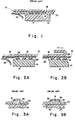
- FIGURE 1 is a cross-sectional view of a conventional dry film used for forming a solder mask, shown being applied to a printed circuit board.
- FIGURE 2A is a cross-sectional view of a dry film in accordance with the invention used for forming a solder mask.
- FIGURE 2B shows removal of the cover sheet from a dry film tacked to a printed circuit board.
- FIGURE 3A is a cross-sectional view of a trace on a printed circuit board covered by a solder mask formed from a prior art, liquid photoimageable composition.
- FIGURE 3B is a cross-sectional view of an alternative trace on a printed circuit board covered by a solder mask formed from a prior art, liquid photoimageable composition.
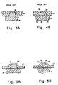
- FIGURE 4A is a cross-sectional view of a trace on a printed circuit board covered by a solder mask formed from a prior art, conventional dry film.
- FIGURE 4B is a cross-sectional view of an alternative trace on a printed circuit board over which a solder mask formed from a prior art, conventional dry film is applied.
- FIGURE 5A is a cross-sectional view of a trace on a printed circuit board encapsulated by a solder mask formed from a dry film in accordance with the present invention.
- FIGURE 5B is a cross-sectional view of an alternative trace on a printed circuit board encapsulated by a solder mask formed from a dry film in accordance with the present invention.
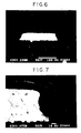
- FIGURES 6-9 are each photographs of a perpendicular slice of a printed circuit board having a solder mask prepared using a dry film in accordance with the present invention, the photographs being taken at an angle of 60° relative to the plane of the board so as to show both the cross-section of the board and the outer surface of the photomask.
- Figure 6 is a 300x magnification of a 50 ⁇ m trace covered with a 50 ⁇ m solder mask.
- Figure 7 is a 750x magnification of a 75 ⁇ m trace covered with a 50 ⁇ m solder mask.
- Figure 8 is a 300x magnification of a 50 ⁇ m trace having lateral overhangs and being covered with a 50 ⁇ m solder mask.
- Figure 9 is a 100x magnification of 50 ⁇ m traces covered with a 50 ⁇ m solder mask.
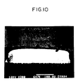
- FIGURE 10 is a 300x magnification of a primary photoresist applied by the method of the present invention over a circuit board having traces.
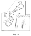
- FIGURE 11 is a diagrammatic illustration of the use of roller apparatus to tack down a dry film to a board.
- FIGURE 12 is a diagrammatic illustration of the use of a roller to conform layers of dry film, from which the cover sheet has been removed, to the surface of a board.
- FIGURE 13A, 13B and 13C illustrate diagramatically a vacuum applicator and a platen operation sequence thereof.
- FIGURE 1 Illustrated in FIGURE 1 is an illustration of a circuit board 10 being covered with a prior art dry film 12.
- the circuit board comprises a board 14 of non-conductive material, e.g., formed of epoxy, and the conductive traces 16 which comprise the printed circuit.
- the dry film comprises a cover sheet 18 of flexible, but generally non-conforming material, typically a polyester, such as polyethylene terephthalate, a layer 20 of photoimageable material which eventually is processed to become the solder mask and a protective sheet 22 formed, for example, of polyethylene.
- the dry film is supplied from a reel 2 ( Figure 11) to the circuit board 10.
- the protective sheet 22 is peeled away, as shown, e.g., by rolling onto a take-up reel 4 ( Figure 11).
- the photoimageable layer is applied to the surface of the circuit board 10, it is laminated thereto with heat, mechanical pressure and vacuum.
- the cover sheet 18 is flexible, it is non-conforming and therefore retains its flat configuration when the dry film 12 is applied to the circuit board 10.
- the photoimageable composition layer 20 during lamination conforms at its contact surface to the circuit board from which the traces 16 protrude; however, the surface of the photoimageable composition layer which is in contact with the cover sheet 18 remains flat.
- the photoimageable composition layer 20 may fully encapsulate the traces 16, it must be thicker than the elevation of the traces above the board 14 of non-conductive material. Standard requirements are that the thickness of the solder mask over all portions of the traces be at least 18 ⁇ m. Because the great majority of traces are elevated 50 ⁇ m or more above the surface of the board 14, the photoimageable composition layer must usually be 68 ⁇ m or thicker. Conventional dry films 12 for forming solder masks typically have photoimageable layers 100 ⁇ m thick.
- FIGURE 2A Illustrated in FIGURE 2A is a dry film 21 in accordance with the present invention.
- This dry film 21 also includes a cover sheet 18, a layer 20 of photoimageable composition which is processable to form a hard, permanent solder mask and an optional, but preferred, protective sheet 22.
- the dry film 21 includes a top coat 24 intermediate the cover sheet 18 and the photoimageable composition layer 20.
- the material for the top coat 24 is selected to have selective adherence to the photoimageable composition layer 20 relative to its adherence to the cover sheet 18, whereby the cover sheet may be peeled away from the remaining layers 20, 24 of the circuit board-adhered dry film, leaving the top coat 24 protecting the photoimageable composition layer 20.
- the top coat 24 is formed of material which also is selected for oxygen-impermeability, whereby it protects the underlying layer of photoimageable composition 20 from oxygen inhibition during free radical photopolymerization in the exposure step.
- the top coat is also selected to be soluble in the developer for the photoimageable composition, whereby the top coat is removed during the development process.
- the top coat material is further selected for transparency, strength and flexibility.
- Dry film for applying photoresist layers having a similar configuration are described in US-A- 4,530,896, FR-A- 2081665 and EP-A- 0267806 US-A- 4,530,896 is limited to application of very thin resist coatings.
- Primary photoresists are typically applied to a metal-covered substrate in order to define the pattern of circuitry traces on a printed circuit board.
- a dry film is described having, in order, a cover sheet, an intermediate layer which acts as a top coat after removal of the cover sheet, a photoresist composition layer and an (optional) protective sheet.
- the main advantages of a solder mask dry film having this laminate arrangement are achieved through the application of the solder mask by the novel process of the present invention.
- the novel process of the present invention closely conforms the photoimageable composition layer 20, which eventually forms the solder mask, to the contours of a circuit board surface which are irregular due to the elevated traces.
- a primary imaging photoresist layer is usually applied to a substantially flat surface.
- the protective sheet 22 is initially peeled from the photoimageable composition layer 20, and the exposed surface of the photoimageable composition layer is applied over a surface of the printed circuit board as seen in Figure 2A.
- the dry film 21 in accordance with one aspect of the present invention may not be fully laminated to the board at the time of application. Rather, slight pressure is used to tack the dry film 21 to the board. Either cold-tacking or hot-tacking may be used. By cold-tacking is generally meant at room temperature, e.g., 20-25°C. Hot-tacking may be at temperatures up to about 70°C.
- the dry film 21 is not tacked to the entire surface, but only to a portion sufficient to provide adequate adherence to the board so as to allow removal of the cover sheet 18 without removal of the remaining layers 20, 24 of the dry film 21 from the circuit board 10.
- a small portion typically 5% or less of the entire surface area of the dry film which lies over the board
- passageways are left between the dry film 21 and the board 10 for subsequent removal of air by application of vacuum. If the dry film is applied by machine, edges, e.g., the leading and trailing edge, may be tacked. If manually applied, tacking at the corners is sufficient. Mechanical pressure, such as that which may easily be provided by a human finger, is sufficient for tacking.
- a circuit board 10 is carried from left to right by drive rollers 23, and the dry films 21 are caused to travel in synchronous motion along the surface thereof.
- Non-driven rollers 25 are reciprocal upward and downward in the direction of double arrows 6 between vertical positions in contact with the dry film and vertical positions remote from the surface.
- the rollers 25 are brought into contact with the dry film, pressing the dry film onto and tacking the dry film to the leading edge of the board.
- the rollers 25 are immediately reciprocated away from the board to allow the middle regions of the board to pass thereby untouched by the rollers.
- the rollers 25 are again reciprocated into contact with the board to tack the dry films 21 to the trailing edge of the board 10.
- Figure 2B shows a preferred mode of removal in which the cover sheet 18 is peeled back in a plane parallel to the plane of the circuit board 10 (as opposed to lifting in a generally perpendicular direction which would tend to remove the photoimageable layer 20 from the circuit board 10).
- the photoimageable layer 20 with the top coat 24 thereon is now vacuum-laminated at elevated temperature to the board.
- a vacuum of at least 0.3 millibar is used and preferably a vacuum of at least 1 millibar.
- Laminating temperatures range from 40°C to 100°C, a range of 55°C to 80°C being preferred. Because the cover sheet 18 is removed, the two remaining layer (photoimageable layer 20 and top coat 24) conform easily to the contours of the irregular surface of the circuit board 10.
- Such vacuum laminating apparatus 100 is briefly described with respect to Figures 13A, 13B and 13C.
- the apparatus includes an upper stationary platen 102 and a lower movable platen 104.
- an upper resilient blanket 106 associated with the lower platen 104
- a lower resilient blanket 108 associated with the lower platen 104
- the lower platen 104 has a well 109 for carrying a dry film-covered circuit board 10.
- Sealing means in the form of an 0-ring 112 are provided on the lower platen 104 for hermetically sealing the well 109 when the lower platen is brought into contact with the upper platen 102 and its associated blanket 106.
- a shim 108 Also shown in Figures 13A-13C is a shim 108.
- the shim is also formed of resilient material and is used to accommodate boards of different thickness. Several shims may be used, including shims interposed between the upper platen 102 and upper blanket 106.
- the lower platen 104 is reciprocal both horizontally and vertically. With the lower platen 104 out of horizontal alignment with the upper platen 102, the dry film-covered circuit board 10 is placed in the well 109 on top of the lower blanket 108. Then the lower platen 104 is moved vertically into alignment with the upper platen 102, the condition shown in Figure 13A. Next, the lower platen is moved upward until contact is effected between the 0-ring 112 and the upper platen 102 and its associated blanket 106 ( Figure 13B).
- the vacuum in the well region 109 causes the upper resilient blanket 106 to "slap down" against the board 10, pressing the board and dry film layers between the upper and lower blankets 106, 108 as seen in Figure 13C. Finally, the vacuum is released from the well region 109 and the lower platen 104 is removed vertically and then horizontally from the upper platen 102 to allow removal of the laminated board.
- the resilient material of the blankets is a type of rubber, e.g., silicon rubber, or other type of resilient polymeric material.
- the surface of each blanket which contacts the dry film is conventionally texturized to prevent a vacuum bond from forming between the blanket and the cover sheet. In prior art processes, such a bond would cause the cover sheet and possibly underlying layers to tear away from the board when the platen and blanket are withdrawn. Texturization of the blankets may be in the form of surface roughness of the polymeric material itself or it may be provided by a rough, rubberized fabric at the dry film contact surface.
- blankets with rough contact surfaces have been found to be disadvantageous if that they leave a negative image imprinted on the remaining layers of dry film.
- new semi-matte blankets have been devised which have a very fine texture. Again, the texture prevents a vacuum bond from being formed between the blanket surface and the remaining layers of the dry film; however, the fine surface texture creates no significant imprint on the remaining, soft layers 20, 24 of the dry film.
- Preferred blanket material is silicon rubber; preferably reinforced with fabric, such as fiberglass.
- the remaining layers 20, 24 conform very closely to the circuit board and provide several advantages which can best be appreciated with respect to FIGURES 3A, 3B, 4A, 4B, 5A, and 5B and the photographs which are FIGURES 6-9.
- the thin layer which comprises the top coat 24 remains fully intact during the conforming process, a result which would not necessarily have been predictable in advance.
- FIGURE 3A illustrates a solder mask which was initially applied as a liquid photoimageable composition.
- the layer Being a liquid, the layer generally conforms to the uneven contours of the circuit board.
- the layer On the top of each trace 16, the layer is of generally uniform thickness; however, in the regions 26 of the knees of the traces, i.e., the lateral edges, the layer greatly thins out, typically being only about 50% as thick as the portion of the layer which covers the flat upper surface of the trace. Frequently, the layer 20 in the regions 26 of the knees is even thinner relative to the portions of the layer on the flat upper surface of the trace.
- FIGURE 3B Illustrated in FIGURE 3B is a solder mask 20 covering a "mushroomed" trace 16' having overhangs 28 on each side. Not only is the solder mask thin in the regions 26 of the knees, but a void, air-filled space 30 is left below each overhang 28.
- FIGURE 4A illustrates a solder mask formed from a photoimageable composition layer 20 of a conventional dry film 12.
- the outer surface of the solder mask has the flat configuration of the cover sheet 18 which was removed subsequent to lamination, while the laminated surface conforms generally to the irregular contours of the circuit board 10.
- the solder mask which is shown in FIGURE 4A is satisfactory from the standpoint of adequately encapsulating the traces 16. It is to be noted, however, that the thickness of the photoimageable composition layer 20 and solder mask formed therefrom is, of necessity, greater than the elevation of the trace, requiring a relatively large amount of photoimageable composition be used to form the layer. This thickness represents a limitation to the resolution of photoimaging which can be achieved.
- FIGURE 4B illustrates a solder mask resulting from a photoimageable layer 20 of a conventional dry film and covering "mushroomed" traces 16' having lateral overhangs 28. Although thickness of the solder mask above the trace 16' is adequate, air-filled voids 30 exist below the overhangs 28.
- FIGURES 5A and 5B illustrate solder masks formed from photoimageable composition layers 20 of dry films 21 produced in accordance with the present invention.
- the remaining layers 20, 24 of the dry film 21 very substantially conform to the irregular surface contours of the circuit board.
- the thickness of the photoimageable layer 20 which was used to form the photomask was equal to or less than the elevation of the trace 16 or 16'; however, the surface of the circuit board is fully covered by the solder mask with the traces 16 or 16' fully encapsulated and encapsulated to an adequate thickness.
- the photomask portions in the regions 26 of the knees of the traces are substantially as thick as photomask portions over the upper flat surfaces of the traces.
- the resulting solder mask has thickness in the regions 26 of the knees of the traces which is at least about 70% of the thickness of the solder mask over the upper flat surface of the traces (over more than about 90% of the linear length of the traces).
- conformance of the layer 20 during vacuum/heat lamination is sufficient to substantially remove air-filled voids from below the overhangs 28. Even though substantial deformation of the photoimageable composition layer 20 is required to achieve this conformance, the top coat 24 maintains its integrity during lamination.
- the solder mask is formed by processing the layer of photoimageable composition in a conventional manner. Artwork is laid over the remaining layers 20, 24 of the dry film; the top coat 24 prevents the artwork from sticking.
- the photoimageable composition layer 20 is exposed to patterned actinic radiation through the protective top coat 24.
- resolution is generally not as critical when developing solder masks as it is in developing photoresist layers
- the thinness of the top coat 24, typically in the range of about 2-3 ⁇ m (as opposed to a cover sheet, typically in the range of about 25 ⁇ m, through which photoimageable composition layers 20 of conventional solder mask-forming dry films 12 must be exposed) contributes to improved resolution. Further contributing to enhanced resolution is the relative thinness of the photoimageable composition layer 20 itself.
- the photoimageable composition layer typically must cover traces 16 with elevation of 50 ⁇ m or more, and the photoimageable composition layers are typically about 100 ⁇ m thick. Because the photoimageable composition layer 20 of the dry film of the present invention is conformable to the surface contours of the circuit board 10, a thickness of 50 ⁇ m or less is sufficient to cover traces elevated 50 ⁇ m and even up to about 75 ⁇ m above the flat surface of the board 14. Of course, a further advantage is substantially reduced levels of expensive photoimageable composition used to form the layer 20.
- solder mask which forms in the regions between the traces 16 is generally at or below the level of the traces.
- slight elevated regions exist between the traces. Such elevated regions may result in the component, which is being soldered, sitting high on the solder mask and preventing pins of the component from being adequately soldered to exposed trace portions.
- the elevated regions may, during reflow, result in some of the pins of a soldered component breaking contact, causing the component to stand up at one end, an effect known as "tombstoning". Inadequate soldered contact and "tombstoning" are avoided when “valleys" instead of elevated regions exist between exposed portions of the traces.
- the layers 20 and 24 are developed, the developer removing the top coat 24 and appropriate portions of the photoimaged layer 20.
- dry film solder mask of this invention has the same ability to "tent" via holes as conventional primary imaging or solder masks films. This is a very important part of the process and cannot be duplicated with simple liquid processes.
- the present invention is not primarily directed to materials from which the various sheets and layers are formed; and reference is again made to US-A- 4,530,896 and EP-A- 0267806.
- the cover sheet 18 is generally formed of a polyester, such as PET and is generally at least about 25 ⁇ m, or thicker, and up to about 75 ⁇ m thick.
- PET if used for the support sheet, is preferably surface-treated to provide adequate hydrophilicity or wetting angle so that it does not adhere strongly to the top coat.
- the wetting or contact angle of the cover sheet material is at least about 60° and is preferably 75° or less.
- One suitable PET cover sheet is sold under the trade designation Melinex-393 by ICI. This is a PET that is surface-treated on one side to enhance its hydrophilicity, i.e., increase its wetting angle.
- cover sheet materials include, but are not limited to polyamides, polyolefins, vinyl polymers, and cellulose esters.
- Any photoimageable composition suitable for forming solder masks is suitable for practice of the invention.
- the protective sheet 22 is selected to be removable from the photoimageable composition layer 20, and is typically a polyethylene sheet, between 15 ⁇ m and 35 ⁇ m thick.
- the top coat 24 is formed of a material which provides the requisite selective adherence.
- the top coat is from 1 to 5 ⁇ m thick, preferably at least 2 ⁇ m.
- a suitable top coat consists essentially of (a) between 10 weight percent and 100 weight percent of either polyvinyl alcohol hydrolyzed to at least 75% or a copolymer formed by the copolymerization of between 95 and 99 molar percent of polyvinyl acetate and between 1 and about 5 molar percent of alkyl ester of acrylic acid and being hydrolyzed to at least 75 percent; (b) up to 90 weight percent of hydroxyethyl cellulose; and (c) up to 10 weight percent of plasticizer.
- hydroxyethyl cellulose is used at a level of at least 25 wt. percent and more preferably at a level of at least 50 wt. percent.
- copolymers are sold under the trade designation VINOL-118 M by Air Products, and 4 weight percent solutions of these copolymers and have viscosities ranging from 5 to 65 MPas at 20°C. PVC homopolymers of similar viscosity are useful as well. Commercially suitable PVA's are also sold by Air Products.
- plasticizer if used, tends to lower the tack temperature of the top coat composition, and tack temperatures below 100°C have been achieved using such plasticizers.
- a top coat composition having a lower tack temperature is easier to adhere to the photoimageable layer.
- Preferred plasticizers are low molecular weight compounds, e.g., below 200, having two or more hydroxyl groups, such as glycerine, ethylene glycol and propylene glycol. While plasticizers desirably lower the tack temperature, they also increase oxygen permeability of the top coat; accordingly amounts of plasticizers in excess of 10% by weight are desirably avoided.
- top coat use include, but are not limited to, the group consisting of polyvinyl ether-maleic anhydride copolymers, water-soluble cellulose ethers, water-soluble salts of carboxyalkylcellulose, water-soluble salts of carboxyalkyl starch, polyvinyl alcohol, polyvinyl pyrrolidone, various polyacrylamides, various water-soluble polyamides, water-soluble salts of polyacrylic acid, gelatin, ethylene oxide polymers, various starches and the like.
- polyvinyl ether-maleic anhydride copolymers water-soluble cellulose ethers, water-soluble salts of carboxyalkylcellulose, water-soluble salts of carboxyalkyl starch, polyvinyl alcohol, polyvinyl pyrrolidone, various polyacrylamides, various water-soluble polyamides, water-soluble salts of polyacrylic acid, gelatin, ethylene oxide polymers, various starches and the like.
- the method of forming the dry film is according to known procedures.
- the top coat and photoimageable composition layers are successively layered on the cover sheet by methods, such as roller coating or by spraying solutions or dispersions of the materials.
- a dry film may be laminated both before and after removal of the cover sheet.
- the photoimageable layer is about equal in thickness or of lesser thickness than the traces (or other unevenness of the board)
- a conventional lamination of such a dry film using heat, vacuum and mechanical slap-down in a conventional manner results in tacking of the photoimageable layer to the upper surfaces of the traces (or other elevations) without penetration of the traces (or elevations) through the photoimageable layer.
- the tacking of the dry film over a greater area of the board facilitates its adhesion to the board during cover sheet removal.
- a second vacuum lamination with heat, vacuum, and mechanical slap-down after cover sheet removal acts to conform the photoimageable composition layer (and top coat) to the contours of the uneven board surface.
- the lamination subsequent to cover sheet removal is for about half the time as the lamination prior to cover sheet removal, e.g., 30 seconds for the second lamination compared to 60 seconds for the first laminations.
- the additional tacking afforded by the initial lamination may prove to be particularly advantageous when using automated equipment for cover sheet removal.
- a roller applying mechanical pressure may be used to accomplish the same purpose. Illustrated diagrammatically in Figure 12 is the use of the roller used to conform a photoimageable layer 20 and top coat 24 to the contours of the board.
- the board 10 and layers 20, 24 of a dry film are moved from left to right below a non-driven roller 45 with the roller in pressure bearing contact with the top coat 24.
- the dry film is first tacked down.
- the dry film is then vacuum laminated to the board 10.
- the layers 20, 24 of the dry film for the most part sit on the top surfaces of the traces 16 as seen at the left-hand side of Figure 12.
- the photoimageable composition 20 and top coat 24 conform to the contours of the board 10 with traces 16 as seen on the right-hand side of Figure 12.
- the layers 20, 24 are pressed down across the full surface of the board 10 as the board passes below the roller.
- a roller could be drawn across the surface of a stationary board.
- the roller 45 used for this purpose should apply between 1 bar and 6 bar pressures.
- the roller 45 is heated depending on the particular application to between 40 and 110°C, generally in the range of 60 to 80°C.
- the surface of the conforming roller 45 has some resiliency, preferably being a polymeric material having a Shore A hardness of between 60 and 80.
- the surface of the roller is smooth.
- the relative speed of the roller 45 and board 10 will vary according to the application, generally between 1 and 10 meters per second, 3 meters per second being typical.
- a dry film is prepared in accordance with,the invention having a cover sheet which is a 50 ⁇ m thick sheet of PET, a 2.5 ⁇ m top coat which is 10 weight percent of the hydrolyzed polyvinyl acetate/acrylic acid copolymer described above, and 90 weight percent hydroxyethyl cellulose, a photoimageable composition forming a layer 50 ⁇ m thick and a polyethylene protective sheet 25 ⁇ m thick.
- the photoimageable composition is formulated as follows: Ingredients: Weight % Chemical Name or Trade Name 36.5 Scripset 540 (styrene/Maleic Anhydride Co-Polymer 25.8 MEK 1.2 Pigment CI 7426 0.05 Sterically hindered phenol anti-oxidant 7.54 Tripropylene glycol diacrylate 3.76 Tripropylene propane triacrylate 0.33 Adhesion Promoter of the Thiazole type 2.81 N-Methylolacrylamide 2.26 Dimethoxyphenyl Acetophenone 0.56 Coating Aid 1.18 Methyl Ethyl Ketone 18.01 Fillers 100%
- a dry film is prepared in accordance with Example 1, using LAMINAR R DM to form the photoimageable composition layer.
- Example 2 Panels having copper traces and plates having tin/lead traces were each cleaned in a conventional manner.
- the dry film of Example 2 was applied to the boards both manually and with an automated system. Manually, the polyethylene protective sheet was removed and the four corners of the film were tacked down with only finger pressure. Using tape to obtain a grip, the cover sheet was removed by drawing off the PET cover sheet in a plane parallel to the board surface.
- a Dynachem DFSM Model 360 laminator was used.
- the Dynachem apparatus uses an "off contact" method which automatically removes the polyethylene protective sheet, tacks down the leading edge of the dry film and then tacks down the trailing edge of the dry film. Application was to both sides of the boards. Then the cover sheet was removed.
- Lamination was effected at a platen temperature of 70°C with a cycle time of 60 seconds and a vacuum of 2 millibars. Mechanical slapdown was for 6 seconds at a vacuum of 0.3 millibar. The boards were held 20-30 minutes.
- FIGURE 6 shows a solder mask formed from a 50 ⁇ m layer encapsulating a 50 ⁇ m trace.
- FIGURE 7 shows a solder mask formed from 50 ⁇ m layer encapsulating a 75 ⁇ m high trace. Excellent coverage at the regions of the knees is seen.
- FIGURE 8 shows a solder mask formed from a 50 ⁇ m layer encapsulating a 50 ⁇ m high trace having overhangs. Solder mask material filling the regions below the overhangs is seen.
- FIGURE 9 shows a solder mask formed from a 50 ⁇ m layer encapsulating 50 ⁇ m high trace. Conformance of the solder mask to the contours of the circuit board is seen.
- a dry film is prepared in accordance with Example 1, using Laminar R AX to form a photoimageable composition layer.
- the resist was laminated over raised connector tabs, as per Example 3, and exposed to an image to a solid copper 7-9 on a Stouffer R 21 Step Sensitivity guide. A covered trace is seen in Figure 10.
- the exposed panel was then developed in a Chemcut 547 spray developer containing 91 liters water, 3% by weight potassium carbonate and 1 to 5% Butyl Cellosolve R which bared about 3/4 of each connector pad. Developer temperature was held between 27-33°C. After thorough rinsing, the board given a 7.6 ⁇ m (0.30 mil) nickel strike followed by 30 min. gold plating cycle in a Technic RC-80 bath.
- the resist was then stripped in a 3-5% NaOH at 54-60°C.
- the gold plated tabs were then inspected for wicking in the areas around which the resist had conformed. No traces of Au or Ni were found anywhere above the gold plated areas. A control, not vacuum laminated in this fashion, showed wicking on about 25% of the tabs.
- the excellent conformability achieved by the laminated dry film in accordance with the present invention might also be achieved with a dry film comprising a layer of photoimageable material backed by a cover sheet of deformable material, e.g., heat-conforming vacuum film.
- a dry film comprising a layer of photoimageable material backed by a cover sheet of deformable material, e.g., heat-conforming vacuum film.
- a cover sheet of deformable material
- a flexible sheet e.g., Tedlar or Teflon®
- Tedlar or Teflon® a flexible sheet
- Tedlar or Teflon® a flexible sheet
- the flexible sheet conforms to the top coat, but can be and is removed prior to or after exposure to allow development.
- a reason for applying such a flexible sheet is to lengthen the permissible period of time between lamination and exposure of the photoimageable layer.
- Flexible sheet material may be a polymeric material or a thin sheet of paper.
Landscapes
- Engineering & Computer Science (AREA)
- Physics & Mathematics (AREA)
- General Physics & Mathematics (AREA)
- Manufacturing & Machinery (AREA)
- Structural Engineering (AREA)
- Mechanical Engineering (AREA)
- Architecture (AREA)
- Microelectronics & Electronic Packaging (AREA)
- Fluid Mechanics (AREA)
- Non-Metallic Protective Coatings For Printed Circuits (AREA)
- Manufacturing Of Printed Circuit Boards (AREA)
- Internal Circuitry In Semiconductor Integrated Circuit Devices (AREA)
- Semiconductor Memories (AREA)
- Electrodes Of Semiconductors (AREA)
- Photosensitive Polymer And Photoresist Processing (AREA)
Abstract
Description
and in that the cover sheet is removed from the top coat after the tacking step (c) and before the lamination step (d), leaving the top coat covering and protecting the photoimageable layer as it is laminated.
| Ingredients: | |
| Weight % | Chemical Name or Trade Name |
| 36.5 | Scripset 540 (styrene/Maleic Anhydride Co-Polymer |
| 25.8 | MEK |
| 1.2 | Pigment CI 7426 |
| 0.05 | Sterically hindered phenol anti-oxidant |
| 7.54 | Tripropylene glycol diacrylate |
| 3.76 | Tripropylene propane triacrylate |
| 0.33 | Adhesion Promoter of the Thiazole type |
| 2.81 | N-Methylolacrylamide |
| 2.26 | Dimethoxyphenyl Acetophenone |
| 0.56 | Coating Aid |
| 1.18 | Methyl Ethyl Ketone |
| 18.01 | Fillers |
| |
Claims (8)
- A method of making a composite comprising a non-conductive substrate having circuitry traces thereon an a layer of a photoimageable composition overlying said traces, comprising the steps of:characterised in that the dry film (21) comprises, between the cover sheet (18) and the photoimageable composition layer (20), a top coat (24) which is selectively adherent to the photoimageable composition relative to its adherence to the cover sheet, said top coat having a thickness of 1 to 5 µm, being soluble in a developer to the photoimageable composition layer and forming a continuous oxygen barrier layer,a) providing a non-conducting substrate (10) having a flat surface with circuitry traces (16) extending upwards from said flat surface;b) laying over said surface a dry film (21) comprising a cover sheet (18) and a layer (20) of a photoimageable composition having an average thickness equal to or less than the height of said circuitry traces above said surface, said composition being soluble in a developer and capable of being rendered insoluble in the developer when exposed to actinic radiation, and being curable after sequential steps of exposure to patterned actinic radiation and development in the developer to provide a hard, permanent solder mask overlying said non-conducting substrate;c) tacking said photoimageable composition layer to said surface andd) laminating the photoimageable composition layer to the surface of said printed circuit board, using heat and vacuum and/or mechanical pressure to conform the layer to the surface and encapsulate the circuitry traces to a thickness of at least 18 µm,
and in that the cover sheet is removed from the top coat after the tacking step (c) and before the lamination step (d), leaving the top coat covering and protecting the photoimageable layer as it is laminated. - A method according to claim 1 wherein said laminating step (D) is carried out by causing a heated roller to pass across the photoimageable layer, applying pressure thereto.
- A method according to claim 1 or claim 2 wherein the photoimageable layer is first laminated to the surface of the printed circuit board, using heat, vacuum and mechanical pressure, prior to removal of the cover sheet from the top coat.
- A method according to any preceding claim wherein the following additional steps are carried out to produce a photoimaged layer on the surface of the printed circuit board:(E) exposing said photoimageable composition layer to patterned actinic radiation; and(F) developing said photoimageable composition to remove unexposed portions from said printed circuit board, leaving either exposed portions remaining on said substrate surface.
- A method according to claim 4 wherein said remaining portions of the photoimageable composition layer are cured to form a hard, permanent solder mask on the surface of the printed circuit board.
- A method according to claim 4 or claim 5 wherein said photoimageable layer (20) is developed in an alkaline aqueous solution and said oxygen-barrier layer (24) is soluble in the alkaline aqueous solution.
- A method according to any preceding claim wherein said circuitry traces (16') have flat upper surfaces and lateral knees (28), the thickness of said photoimageable composition layer in the region of said lateral knees being at least 70% of the thickness of said photoimageable composition layer over the top surfaces of said circuitry traces over about 90% of the linear extent of said circuitry traces.
- A method according to any preceding claim wherein said photoimageable composition layer (20) and said continuous oxygen-barrier layer are vacuum-conformed to said non-conducting substrate (14) and said upwardly extending circuitry traces (16).
Applications Claiming Priority (4)
| Application Number | Priority Date | Filing Date | Title |
|---|---|---|---|
| US07/160,895 US4889790A (en) | 1988-02-26 | 1988-02-26 | Method of forming a conformable mask on a printed circuit board |
| US07/264,472 US4992354A (en) | 1988-02-26 | 1988-10-28 | Dry film photoresist for forming a conformable mask and method of application to a printed circuit board or the like |
| US264472 | 1988-10-28 | ||
| US160895 | 2002-06-03 |
Publications (3)
| Publication Number | Publication Date |
|---|---|
| EP0330339A2 EP0330339A2 (en) | 1989-08-30 |
| EP0330339A3 EP0330339A3 (en) | 1991-11-27 |
| EP0330339B1 true EP0330339B1 (en) | 1998-04-29 |
Family
ID=26857314
Family Applications (1)
| Application Number | Title | Priority Date | Filing Date |
|---|---|---|---|
| EP89301228A Expired - Lifetime EP0330339B1 (en) | 1988-02-26 | 1989-02-09 | Method of forming conformable masks |
Country Status (11)
| Country | Link |
|---|---|
| US (1) | US4992354A (en) |
| EP (1) | EP0330339B1 (en) |
| JP (1) | JPH0666031B2 (en) |
| KR (1) | KR920008720B1 (en) |
| AT (1) | ATE165674T1 (en) |
| AU (1) | AU625637B2 (en) |
| CA (1) | CA1304169C (en) |
| DE (1) | DE68928654T2 (en) |
| DK (1) | DK89089A (en) |
| ES (1) | ES2116967T3 (en) |
| SG (1) | SG52247A1 (en) |
Families Citing this family (28)
| Publication number | Priority date | Publication date | Assignee | Title |
|---|---|---|---|---|
| US4946524A (en) * | 1989-03-02 | 1990-08-07 | Morton International, Inc. | Applicator and method for applying dry film solder mask on a board |
| CA2034601A1 (en) * | 1990-02-12 | 1991-08-13 | James Briguglio | Solder mask vacuum laminator conversion |
| CA2034623A1 (en) * | 1990-02-16 | 1991-08-17 | Ming Tara | Photoimageable compositions containing fugitive colorants |
| JPH0450852A (en) * | 1990-06-14 | 1992-02-19 | Hitachi Chem Co Ltd | Photosensitive film and forming method for solder mask using its film |
| JPH04146687A (en) * | 1990-10-08 | 1992-05-20 | Nippon Paint Co Ltd | Manufacture of solder masked circuit board |
| IT1250461B (en) * | 1991-08-09 | 1995-04-07 | Morton Int Inc | PROCEDURE AND APPARATUS TO APPLY CONTINUOUS WAYS IN PARTICULAR WELDING MASKS ON PANELS OF PRINTED CIRCUITS. |
| US5270146A (en) * | 1992-04-07 | 1993-12-14 | Morton International, Inc. | Photosensitive laminate having dual intermediate layers |
| IT1274181B (en) * | 1994-05-18 | 1997-07-15 | Amedeo Candore | LAMINATION OF PHOTOSENSITIVE FILMS TO FORM A WELDING MASK ON PRINTED CIRCUIT BOARDS |
| TW283819B (en) * | 1995-02-03 | 1996-08-21 | Fuji Photo Film Co Ltd | |
| US5609991A (en) * | 1995-02-10 | 1997-03-11 | Morton International, Inc. | Photoimageable composition having improved alkaline process resistance and tack-free surface for contact imaging |
| US5626774A (en) * | 1995-12-11 | 1997-05-06 | Alliedsignal Inc. | Solder mask for manufacture of printed circuit boards |
| US5993945A (en) * | 1996-05-30 | 1999-11-30 | International Business Machines Corporation | Process for high resolution photoimageable dielectric |
| US6022670A (en) * | 1997-05-08 | 2000-02-08 | International Business Machines Corporation | Process for high resolution photoimageable dielectric |
| US6057079A (en) * | 1997-09-24 | 2000-05-02 | Shipley Company, L.L.C. | Dry film photoresist construction suitable for rolling up on itself |
| DE19820049C2 (en) * | 1998-05-05 | 2001-04-12 | Epcos Ag | Thermomechanical method for the planarization of a layer that can be structured using photo technology, in particular encapsulation for electronic components |
| US6090474A (en) * | 1998-09-01 | 2000-07-18 | International Business Machines Corporation | Flowable compositions and use in filling vias and plated through-holes |
| US6542379B1 (en) | 1999-07-15 | 2003-04-01 | International Business Machines Corporation | Circuitry with integrated passive components and method for producing |
| IT1313117B1 (en) * | 1999-08-25 | 2002-06-17 | Morton Int Inc | VACUUM APPLICATION EQUIPMENT EQUIPPED WITH CONVEYING VEHICLES PROCEDURE FOR APPLYING A DRY FILM RESIST TO A PANEL OF |
| IT1313118B1 (en) | 1999-08-25 | 2002-06-17 | Morton Int Inc | VACUUM APPLICATION EQUIPMENT EQUIPPED WITH CONVEYING MEANS PROCEDURE FOR APPLYING A DRY FILM RESIST TO A PANEL |
| EP1117006A1 (en) * | 2000-01-14 | 2001-07-18 | Shipley Company LLC | Photoresist having increased photospeed |
| US6329609B1 (en) | 2000-06-29 | 2001-12-11 | International Business Machines Corporation | Method and structure to prevent distortion and expansion of organic spacer layer for thin film transfer-join technology |
| US7148265B2 (en) * | 2002-09-30 | 2006-12-12 | Rohm And Haas Electronic Materials Llc | Functional polymer |
| US7323290B2 (en) * | 2002-09-30 | 2008-01-29 | Eternal Technology Corporation | Dry film photoresist |
| US7741003B2 (en) * | 2004-03-30 | 2010-06-22 | Hitachi Global Storage Technologies Netherlands B.V. | Photoresist transfer pads |
| JP5316901B2 (en) * | 2009-12-07 | 2013-10-16 | 山栄化学株式会社 | Printed wiring board and manufacturing method thereof |
| CN102799070B (en) * | 2012-08-27 | 2014-03-05 | 珠海市能动科技光学产业有限公司 | Double coating negative photoresist dry film |
| EP3035122B1 (en) | 2014-12-16 | 2019-03-20 | ATOTECH Deutschland GmbH | Method for fine line manufacturing |
| CN118963064B (en) * | 2024-10-16 | 2025-01-24 | 中国工程物理研究院激光聚变研究中心 | A method for preparing a thick photoresist microstructure |
Citations (1)
| Publication number | Priority date | Publication date | Assignee | Title |
|---|---|---|---|---|
| US4413051A (en) * | 1981-05-04 | 1983-11-01 | Dynamics Research Corporation | Method for providing high resolution, highly defined, thick film patterns |
Family Cites Families (9)
| Publication number | Priority date | Publication date | Assignee | Title |
|---|---|---|---|---|
| DE2106574A1 (en) * | 1970-03-03 | 1971-09-23 | Shpley Co Inc | Photosensitive laminate |
| US4530896A (en) * | 1970-03-03 | 1985-07-23 | Shipley Company Inc. | Photosensitive laminate |
| DE2544553C2 (en) * | 1974-10-08 | 1983-08-04 | E.I. du Pont de Nemours and Co., 19898 Wilmington, Del. | Process for applying a photopolymerizable solid resist layer to a substrate |
| US4127436A (en) * | 1975-04-17 | 1978-11-28 | E. I. Du Pont De Nemours And Company | Vacuum laminating process |
| JPS593740B2 (en) * | 1975-07-30 | 1984-01-25 | 日立化成工業株式会社 | Manufacturing method of solid plate with photosensitive layer formed on uneven surface |
| EP0003801B1 (en) * | 1978-02-17 | 1982-06-09 | E.I. Du Pont De Nemours And Company | Use of photosensitive stratum to create through-hole connections in circuit boards |
| JPS55501072A (en) * | 1978-12-25 | 1980-12-04 | ||
| US4495014A (en) * | 1983-02-18 | 1985-01-22 | E. I. Du Pont De Nemours And Company | Laminating and trimming process |
| JPS6252552A (en) * | 1985-08-30 | 1987-03-07 | Hitachi Chem Co Ltd | Method and device for vacuum sticking |
-
1988
- 1988-10-28 US US07/264,472 patent/US4992354A/en not_active Expired - Lifetime
-
1989
- 1989-02-09 AT AT89301228T patent/ATE165674T1/en not_active IP Right Cessation
- 1989-02-09 DE DE68928654T patent/DE68928654T2/en not_active Expired - Fee Related
- 1989-02-09 SG SG1996001284A patent/SG52247A1/en unknown
- 1989-02-09 EP EP89301228A patent/EP0330339B1/en not_active Expired - Lifetime
- 1989-02-09 ES ES89301228T patent/ES2116967T3/en not_active Expired - Lifetime
- 1989-02-15 AU AU29961/89A patent/AU625637B2/en not_active Ceased
- 1989-02-24 DK DK089089A patent/DK89089A/en not_active Application Discontinuation
- 1989-02-24 CA CA000591968A patent/CA1304169C/en not_active Expired - Lifetime
- 1989-02-25 KR KR8902305A patent/KR920008720B1/en not_active Expired
- 1989-02-27 JP JP1043376A patent/JPH0666031B2/en not_active Expired - Lifetime
Patent Citations (1)
| Publication number | Priority date | Publication date | Assignee | Title |
|---|---|---|---|---|
| US4413051A (en) * | 1981-05-04 | 1983-11-01 | Dynamics Research Corporation | Method for providing high resolution, highly defined, thick film patterns |
Non-Patent Citations (1)
| Title |
|---|
| Encyclopedia of Chemical Technology, Kirk-Othmer, vol. 3, pages 480-502 * |
Also Published As
| Publication number | Publication date |
|---|---|
| KR920008720B1 (en) | 1992-10-08 |
| SG52247A1 (en) | 1998-09-28 |
| DK89089D0 (en) | 1989-02-24 |
| ATE165674T1 (en) | 1998-05-15 |
| ES2116967T3 (en) | 1998-08-01 |
| AU2996189A (en) | 1989-08-31 |
| EP0330339A3 (en) | 1991-11-27 |
| CA1304169C (en) | 1992-06-23 |
| DK89089A (en) | 1989-08-27 |
| AU625637B2 (en) | 1992-07-16 |
| US4992354A (en) | 1991-02-12 |
| DE68928654T2 (en) | 1998-08-20 |
| JPH026960A (en) | 1990-01-11 |
| JPH0666031B2 (en) | 1994-08-24 |
| DE68928654D1 (en) | 1998-06-04 |
| EP0330339A2 (en) | 1989-08-30 |
Similar Documents
| Publication | Publication Date | Title |
|---|---|---|
| US4992354A (en) | Dry film photoresist for forming a conformable mask and method of application to a printed circuit board or the like | |
| US4889790A (en) | Method of forming a conformable mask on a printed circuit board | |
| US5213945A (en) | Dry film photoresist for forming a conformable mask and method of application to a printed circuit board or the like | |
| US4506004A (en) | Printed wiring board | |
| US4260675A (en) | Photoprinting plate and method of preparing printed circuit board solder masks therewith | |
| US6585837B1 (en) | Conveyorized vacuum applicator and method of applying a dry film resist to a printed circuit board | |
| KR100417081B1 (en) | Vacuum laminating equipment and hot lamination • | |
| JPH0426464B2 (en) | ||
| US20040261941A1 (en) | Method of vacuum-laminating adhesive film | |
| EP0141868A1 (en) | High resolution phototransparency image forming with photopolymers | |
| US5164284A (en) | Method of application of a conforming mask to a printed circuit board | |
| CA1260266A (en) | Method for creating a design in relief in a hard smooth substrate and apparatus for use in the method | |
| EP0267600B1 (en) | Method for selectively curing a liquid photosensitive resin by masking exposure | |
| JPS593740B2 (en) | Manufacturing method of solid plate with photosensitive layer formed on uneven surface | |
| EP0188051B1 (en) | Transfer sheet | |
| US4954421A (en) | Photoflashing a liquid polymer layer on a phototool surface exposed to air | |
| AU605011B2 (en) | Method of and apparatus for applying polymeric materials to printed circuits | |
| JPH0314334B2 (en) | ||
| US5753414A (en) | Photopolymer plate having a peelable substrate | |
| US4727013A (en) | Method for creating a design in relief in a hard smooth substrate and apparatus for use in the method | |
| USRE32430E (en) | Printed wiring board | |
| JPS63296389A (en) | Method of temporarily sealing hole in printed circuit board | |
| EP0382944B1 (en) | Method and structure for preventing wet etchant penetration at the interface between a resist mask and an underlying metal layer | |
| JP4018951B2 (en) | Method for manufacturing printing blanket | |
| NO890656L (en) | DRY MOVIE PHOTO RESIST FOR THE MAKING OF A FORMABLE MASK AND PROCEDURE TO USE A PRINTED CIRCUIT OR LIKE. |
Legal Events
| Date | Code | Title | Description |
|---|---|---|---|
| PUAI | Public reference made under article 153(3) epc to a published international application that has entered the european phase |
Free format text: ORIGINAL CODE: 0009012 |
|
| AK | Designated contracting states |
Kind code of ref document: A2 Designated state(s): AT BE CH DE ES FR GB IT LI NL SE |
|
| RAP1 | Party data changed (applicant data changed or rights of an application transferred) |
Owner name: MORTON INTERNATIONAL, INC. |
|
| 17P | Request for examination filed |
Effective date: 19901214 |
|
| PUAL | Search report despatched |
Free format text: ORIGINAL CODE: 0009013 |
|
| AK | Designated contracting states |
Kind code of ref document: A3 Designated state(s): AT BE CH DE ES FR GB IT LI NL SE |
|
| 17Q | First examination report despatched |
Effective date: 19940810 |
|
| GRAG | Despatch of communication of intention to grant |
Free format text: ORIGINAL CODE: EPIDOS AGRA |
|
| RAP1 | Party data changed (applicant data changed or rights of an application transferred) |
Owner name: MORTON INTERNATIONAL, INC. |
|
| GRAG | Despatch of communication of intention to grant |
Free format text: ORIGINAL CODE: EPIDOS AGRA |
|
| GRAG | Despatch of communication of intention to grant |
Free format text: ORIGINAL CODE: EPIDOS AGRA |
|
| GRAH | Despatch of communication of intention to grant a patent |
Free format text: ORIGINAL CODE: EPIDOS IGRA |
|
| GRAH | Despatch of communication of intention to grant a patent |
Free format text: ORIGINAL CODE: EPIDOS IGRA |
|
| GRAA | (expected) grant |
Free format text: ORIGINAL CODE: 0009210 |
|
| AK | Designated contracting states |
Kind code of ref document: B1 Designated state(s): AT BE CH DE ES FR GB IT LI NL SE |
|
| REF | Corresponds to: |
Ref document number: 165674 Country of ref document: AT Date of ref document: 19980515 Kind code of ref document: T |
|
| REG | Reference to a national code |
Ref country code: CH Ref legal event code: EP |
|
| REG | Reference to a national code |
Ref country code: CH Ref legal event code: NV Representative=s name: KIRKER & CIE SA |
|
| REF | Corresponds to: |
Ref document number: 68928654 Country of ref document: DE Date of ref document: 19980604 |
|
| ITF | It: translation for a ep patent filed | ||
| PG25 | Lapsed in a contracting state [announced via postgrant information from national office to epo] |
Ref country code: SE Free format text: LAPSE BECAUSE OF FAILURE TO SUBMIT A TRANSLATION OF THE DESCRIPTION OR TO PAY THE FEE WITHIN THE PRESCRIBED TIME-LIMIT Effective date: 19980729 |
|
| REG | Reference to a national code |
Ref country code: ES Ref legal event code: FG2A Ref document number: 2116967 Country of ref document: ES Kind code of ref document: T3 |
|
| ET | Fr: translation filed | ||
| PLBE | No opposition filed within time limit |
Free format text: ORIGINAL CODE: 0009261 |
|
| STAA | Information on the status of an ep patent application or granted ep patent |
Free format text: STATUS: NO OPPOSITION FILED WITHIN TIME LIMIT |
|
| 26N | No opposition filed | ||
| REG | Reference to a national code |
Ref country code: GB Ref legal event code: IF02 |
|
| PGFP | Annual fee paid to national office [announced via postgrant information from national office to epo] |
Ref country code: GB Payment date: 20050120 Year of fee payment: 17 |
|
| PGFP | Annual fee paid to national office [announced via postgrant information from national office to epo] |
Ref country code: NL Payment date: 20050215 Year of fee payment: 17 |
|
| PGFP | Annual fee paid to national office [announced via postgrant information from national office to epo] |
Ref country code: FR Payment date: 20050216 Year of fee payment: 17 |
|
| PGFP | Annual fee paid to national office [announced via postgrant information from national office to epo] |
Ref country code: BE Payment date: 20050218 Year of fee payment: 17 Ref country code: AT Payment date: 20050218 Year of fee payment: 17 |
|
| PGFP | Annual fee paid to national office [announced via postgrant information from national office to epo] |
Ref country code: CH Payment date: 20050221 Year of fee payment: 17 |
|
| PGFP | Annual fee paid to national office [announced via postgrant information from national office to epo] |
Ref country code: ES Payment date: 20050224 Year of fee payment: 17 |
|
| PGFP | Annual fee paid to national office [announced via postgrant information from national office to epo] |
Ref country code: DE Payment date: 20050421 Year of fee payment: 17 |
|
| PG25 | Lapsed in a contracting state [announced via postgrant information from national office to epo] |
Ref country code: GB Free format text: LAPSE BECAUSE OF NON-PAYMENT OF DUE FEES Effective date: 20060209 Ref country code: AT Free format text: LAPSE BECAUSE OF NON-PAYMENT OF DUE FEES Effective date: 20060209 |
|
| PG25 | Lapsed in a contracting state [announced via postgrant information from national office to epo] |
Ref country code: ES Free format text: LAPSE BECAUSE OF NON-PAYMENT OF DUE FEES Effective date: 20060210 |
|
| PG25 | Lapsed in a contracting state [announced via postgrant information from national office to epo] |
Ref country code: LI Free format text: LAPSE BECAUSE OF NON-PAYMENT OF DUE FEES Effective date: 20060228 Ref country code: CH Free format text: LAPSE BECAUSE OF NON-PAYMENT OF DUE FEES Effective date: 20060228 Ref country code: BE Free format text: LAPSE BECAUSE OF NON-PAYMENT OF DUE FEES Effective date: 20060228 |
|
| PGFP | Annual fee paid to national office [announced via postgrant information from national office to epo] |
Ref country code: IT Payment date: 20060228 Year of fee payment: 18 |
|
| PG25 | Lapsed in a contracting state [announced via postgrant information from national office to epo] |
Ref country code: NL Free format text: LAPSE BECAUSE OF NON-PAYMENT OF DUE FEES Effective date: 20060901 Ref country code: DE Free format text: LAPSE BECAUSE OF NON-PAYMENT OF DUE FEES Effective date: 20060901 |
|
| REG | Reference to a national code |
Ref country code: CH Ref legal event code: PL |
|
| GBPC | Gb: european patent ceased through non-payment of renewal fee |
Effective date: 20060209 |
|
| NLV4 | Nl: lapsed or anulled due to non-payment of the annual fee |
Effective date: 20060901 |
|
| REG | Reference to a national code |
Ref country code: FR Ref legal event code: ST Effective date: 20061031 |
|
| REG | Reference to a national code |
Ref country code: ES Ref legal event code: FD2A Effective date: 20060210 |
|
| BERE | Be: lapsed |
Owner name: *MORTON INTERNATIONAL INC. Effective date: 20060228 |
|
| PG25 | Lapsed in a contracting state [announced via postgrant information from national office to epo] |
Ref country code: FR Free format text: LAPSE BECAUSE OF NON-PAYMENT OF DUE FEES Effective date: 20060228 |
|
| PG25 | Lapsed in a contracting state [announced via postgrant information from national office to epo] |
Ref country code: IT Free format text: LAPSE BECAUSE OF NON-PAYMENT OF DUE FEES Effective date: 20070209 |