EP0328281B1 - Directable aperture etched in silicon - Google Patents
Directable aperture etched in silicon Download PDFInfo
- Publication number
- EP0328281B1 EP0328281B1 EP89300864A EP89300864A EP0328281B1 EP 0328281 B1 EP0328281 B1 EP 0328281B1 EP 89300864 A EP89300864 A EP 89300864A EP 89300864 A EP89300864 A EP 89300864A EP 0328281 B1 EP0328281 B1 EP 0328281B1
- Authority
- EP
- European Patent Office
- Prior art keywords
- etchant
- pit
- aperture
- planar surface
- planes
- Prior art date
- Legal status (The legal status is an assumption and is not a legal conclusion. Google has not performed a legal analysis and makes no representation as to the accuracy of the status listed.)
- Expired - Lifetime
Links
Images

Classifications
-
- B—PERFORMING OPERATIONS; TRANSPORTING
- B41—PRINTING; LINING MACHINES; TYPEWRITERS; STAMPS
- B41J—TYPEWRITERS; SELECTIVE PRINTING MECHANISMS, i.e. MECHANISMS PRINTING OTHERWISE THAN FROM A FORME; CORRECTION OF TYPOGRAPHICAL ERRORS
- B41J2/00—Typewriters or selective printing mechanisms characterised by the printing or marking process for which they are designed
- B41J2/005—Typewriters or selective printing mechanisms characterised by the printing or marking process for which they are designed characterised by bringing liquid or particles selectively into contact with a printing material
- B41J2/01—Ink jet
- B41J2/135—Nozzles
- B41J2/16—Production of nozzles
- B41J2/1621—Manufacturing processes
- B41J2/1631—Manufacturing processes photolithography
-
- B—PERFORMING OPERATIONS; TRANSPORTING
- B41—PRINTING; LINING MACHINES; TYPEWRITERS; STAMPS
- B41J—TYPEWRITERS; SELECTIVE PRINTING MECHANISMS, i.e. MECHANISMS PRINTING OTHERWISE THAN FROM A FORME; CORRECTION OF TYPOGRAPHICAL ERRORS
- B41J2/00—Typewriters or selective printing mechanisms characterised by the printing or marking process for which they are designed
- B41J2/005—Typewriters or selective printing mechanisms characterised by the printing or marking process for which they are designed characterised by bringing liquid or particles selectively into contact with a printing material
- B41J2/01—Ink jet
- B41J2/135—Nozzles
- B41J2/16—Production of nozzles
-
- B—PERFORMING OPERATIONS; TRANSPORTING
- B41—PRINTING; LINING MACHINES; TYPEWRITERS; STAMPS
- B41J—TYPEWRITERS; SELECTIVE PRINTING MECHANISMS, i.e. MECHANISMS PRINTING OTHERWISE THAN FROM A FORME; CORRECTION OF TYPOGRAPHICAL ERRORS
- B41J2/00—Typewriters or selective printing mechanisms characterised by the printing or marking process for which they are designed
- B41J2/005—Typewriters or selective printing mechanisms characterised by the printing or marking process for which they are designed characterised by bringing liquid or particles selectively into contact with a printing material
- B41J2/01—Ink jet
- B41J2/135—Nozzles
- B41J2/16—Production of nozzles
- B41J2/1621—Manufacturing processes
- B41J2/1626—Manufacturing processes etching
- B41J2/1629—Manufacturing processes etching wet etching
-
- B—PERFORMING OPERATIONS; TRANSPORTING
- B41—PRINTING; LINING MACHINES; TYPEWRITERS; STAMPS
- B41J—TYPEWRITERS; SELECTIVE PRINTING MECHANISMS, i.e. MECHANISMS PRINTING OTHERWISE THAN FROM A FORME; CORRECTION OF TYPOGRAPHICAL ERRORS
- B41J2/00—Typewriters or selective printing mechanisms characterised by the printing or marking process for which they are designed
- B41J2/005—Typewriters or selective printing mechanisms characterised by the printing or marking process for which they are designed characterised by bringing liquid or particles selectively into contact with a printing material
- B41J2/01—Ink jet
- B41J2/135—Nozzles
- B41J2/16—Production of nozzles
- B41J2/1621—Manufacturing processes
- B41J2/1635—Manufacturing processes dividing the wafer into individual chips
-
- H—ELECTRICITY
- H10—SEMICONDUCTOR DEVICES; ELECTRIC SOLID-STATE DEVICES NOT OTHERWISE PROVIDED FOR
- H10P—GENERIC PROCESSES OR APPARATUS FOR THE MANUFACTURE OR TREATMENT OF DEVICES COVERED BY CLASS H10
- H10P50/00—Etching of wafers, substrates or parts of devices
- H10P50/60—Wet etching
- H10P50/64—Wet etching of semiconductor materials
- H10P50/642—Chemical etching
- H10P50/644—Anisotropic liquid etching
Definitions
- the field of the invention relates to etching apertures in monocrystalline substrates such as silicon.
- apertures in silicon substrates by etchant processes commonly referred to as micro-machining. These apertures have been used in optics and also as fluid flow nozzles. Examples of these apertures are enumerated below.
- U.S. Patent 4,269,653 issued to Wada et al discloses an aperture etched through silicon for use as an electron beam exposure device.
- the resulting aperture axis is perpendicular to the nominal plane of the silicon substrate.
- IBM Technical Disclosure Bulletin, Volume 14, No. 2, July 1971, Pages 417-418, entitled “Fabricating Shaped Grid and Aperture Holes”, discloses a method for etching an array of apertures for use as illumination apertures. More specifically, a silicon substrate is shown having an epitaxial layer grown thereon. A desired array or pattern of apertures is etched through the epitaxial layer. An etchant which attacks the silicon substrate, but not the epitaxial layer, is then used to etch the substrate off from the backside thereby exposing the epitaxial layer and the pattern of apertures etched therethrough. Each aperture has an aperture axis perpendicular to the epitaxial layer.
- U.S. Patent 4,169,008 discloses a method of etching apertures for use as nozzles in ink-jet printers.
- Etchant pits in both the top and bottom surfaces form an opening having an aperture axis perpendicular to the nominal plane of the wafer.
- variations in the aperture openings are avoided which would otherwise occur due to variations in the wafer thickness.
- the dimensions of the openings in the bottom planar surface are determined by the bottom mask openings, rather than by the intersection of the top etchant pit with the bottom planar surface.
- Each aperture axis is perpendicular to the nominal plane of the substrate.
- a problem with the above approaches is that the angle of the aperture plane is not selectable.
- the aperture axis is constrained to a direction perpendicular to the nominal plane of the substrate. Additional structure is needed to direct the fluid flow in a direction other than perpendicular to the substrate plane which may be desired for a particular application.
- a method for anisotropically etching a first aperture into a monocrystalline substrate such that the plane of the first aperture is inclined at a selectable angle ( ⁇ ) with respect to the nominal crystalline planes of the substrate comprising the steps of -:
- an advantage of the invention is that the designer may select any aperture angle desired by appropriate selection of the above described values ( ⁇ L, d1, d2 and the type of monocrystalline material ( ⁇ )).
- the desired aperture may require only a single etchant step wherein top and bottom planar surfaces are concurrently etched to the same depth.
- a directable aperture is formed in only a single substrate whereas multiple substrates were heretofore required.
- An additional advantage is that multiple apertures may be formed, each having a different aperture axis, in a single substrate.
- aperture assembly 10 is shown for the purposes of illustrating an example in which the invention is used to advantage.
- Aperture assembly 10 is here shown fabricated from a ⁇ 100 ⁇ silicon substrate 12 which has been sawed from a wafer, by conventional means, such that top planar surface 14 and bottom planar surface 16 lie substantially in the ⁇ 100 ⁇ nominal crystalline plane.
- First etchant pit 20 is shown formed through top planar surface 14 with side walls 22, 24, 26, and 28, and bottom wall 30.
- Side walls 22, 24, 26, and 28 lie in the ⁇ 111 ⁇ intersecting planes which intersect the ⁇ 100 ⁇ nominal plane at an angle ⁇ of approximately 54.7°.
- aperture 40 and aperture 42 are symmetrically positioned in substrate 12.
- the invention may be used to advantage with substrates having major surfaces lying in other planar directions such as, for example, ⁇ 110 ⁇ silicon.
- the invention may be used to advantage with any monocrystalline substrate.
- aperture 40 and aperture 42 are generally defined by the intersection of top etchant pit 20 with respective bottom etchant pit 44 and bottom etchant pit 46.
- bottom etchant pit 44 is defined by side walls 48, 50, 52 (not shown) and 54 (not shown) lying in the ⁇ 111 ⁇ intersecting planes, and top wall 56 lying in the ⁇ 100 ⁇ plane.
- Side walls 48, 50, 52, and 54 are formed at an angle ⁇ with respect to bottom planar surface 16 or the ⁇ 100 ⁇ planes in general.
- Aperture plane 62 of aperture 42 is shown in Figure 2 as a plane between protruding edges 64 and 66 of aperture 42.
- Protruding edge 64 is defined by the intersection of top etchant pit 20 with top wall 56 of bottom etchant pit 44.
- Protruding edge 66 is defined by the intersection of bottom etchant pit 44 with bottom wall 30 of top etchant pit 20.
- Aperture axis 68 of aperture 42 is shown perpendicular to aperture plane 62 midway between protruding edges 64 and 66.
- the angle of the aperture plane with respect to bottom planar surface 16, or the ⁇ 100 ⁇ planes in general, is herein designated as angle ⁇ .
- Aperture 40 is shown in Figure 2 as being symmetrically formed in substrate 12 with respect to aperture 42.
- Bottom etchant pit 46 is having top wall 76 lying in the ⁇ 100 ⁇ plane and side walls 78, 80, 82 (not shown), and 84 (not shown) lying in the ⁇ 111 ⁇ planes.
- Side walls 78, 80, 82 and 84 are etched at an angle ⁇ with respect to bottom planar surface 16 or the ⁇ 100 ⁇ planes in general.
- Aperture plane 92 of aperture 40 is defined as a planar surface between protruding edges 94 and 96 of aperture 40.
- Protruding edge 96 is defined by the intersection of top etchant pit 20 with top wall 76 of bottom etchant pit 46.
- Protruding edge 94 is defined by the intersection of bottom etchant pit 46 with bottom wall 30 of top etchant pit 20.
- Aperture axis 98 of aperture 40 is shown perpendicular to aperture plane 92 midway between protruding edges 94 and 96.
- the angle of aperture plane 92 with respect to top planar surface 14, or the ⁇ 100 ⁇ planes in general, is herein designated as angle ⁇ .
- Substrate 12 is illustrated in Figure 3A as a silicon substrate, preferably having been sawed to a thickness of approximately 200 to 500 microns with major surfaces lying substantially in the ⁇ 100 ⁇ planes.
- Top and bottom silicon oxide layers 102 and 104, respectively, are grown on substrate 12 using conventional techniques well known in the semiconductor industry.
- Layer of silicon nitride 106 and layer of silicon nitride 108 are deposited over respective silicon oxide layers 102 and 104, respectively, using conventional vapor deposition techniques. Silicon oxide layer 102 and silicon nitride layer 106, together define passivation layer 107.
- the combination of silicon oxide layer 104 and silicon nitride layer 108 define passivation layer 109.
- photo-resist layers 112 and 114 are deposited over respective passivation layers 107 and 109.
- Rectangular etchant pattern 116 is delineated in photo-resist layer 112 by conventional photolithographic techniques. Rectangular etchant pattern 116 is etched through passivation layer 107 thereby exposing a corresponding rectangular portion of top planar surface 14 for etching top etchant pit 20 in a subsequent etching step.
- bottom rectangular pattern 126 and bottom rectangular pattern 128 are delineated through bottom photo-resist layer 114 and passivation layer 109.
- a wet anisotropic etchant solution such as aqueous-potassium-hydroxide solution or ethylene-diamine-pyrocatecol solution, is applied to top rectangular pattern 116, bottom rectangular pattern 126, and bottom rectangular pattern 128 to form respective top etchant pit 20, bottom etchant pit 44 and bottom etchant pit 46.
- the wet etchant acts against the ⁇ 100 ⁇ planes at a rate approximately 100 times greater than against the ⁇ 111 ⁇ planes.
- the etchant steps are timed such that top etchant pit 20 is etched against the ⁇ 100 ⁇ planes to a distance d1 before bottom planar surface 16.
- top etchant pit 20 is etched to a depth t-d1 where t is the thickness of substrate 12.
- t is the thickness of substrate 12.
- sidewalls 22, 24, 26 ( Figure 1) and 28 ( Figure 1) which lie in the ⁇ 111 ⁇ planes, are slightly offset from rectangular pattern 116. More specifically, the intersection of sidewalls 22, 24, 26 and 28 with top planar surface 14 defines, respectively, left transverse edge 118, right transverse edge 120, longitudinal edge 122 ( Figure 1), and longitudinal edge 124 ( Figure 1) of etchant pit 20, all of which are slightly offset from rectangular pattern 116.
- Both bottom etchant pit 44 and bottom etchant pit 46 are etched to a depth d2 before top planar surface 14. That is, bottom etchant pit 44 and bottom etchant pit 46 are etched to a depth t-d2.
- bottom etchant pit 44 the intersection of sidewalls 48, 50, 52 (not shown) and 54 (not shown) with bottom planar surface 16 defines, respectively, left transverse edge 130, right transverse edge 132, longitudinal edge 134 (not shown), and longitudinal edge 136 (not shown), all of which are slightly offset from rectangular pattern 126.
- bottom etchant pit 46 the intersection of sidewalls 78, 80, 82 (not shown) and 84 (not shown) with bottom planar surface 16 defines, respectively, left transverse edge 138, right transverse edge 140, longitudinal edge 142 (not shown), and longitudinal edge 144 (not shown), all of which are slightly offset from rectangular pattern 128.
- aperture plane 62 extends through protruding edges 64 and 66 forming angle ⁇ with respect to bottom planar surface 16.
- Side walls 48 and 50 of etchant pit 44 lie along the ⁇ 111 ⁇ planes at an angle ⁇ to the nominal ⁇ 100 ⁇ plane of 54.7°.
- Preselected angle ⁇ is related to the longitudinal distance between left transverse edge 130 of bottom etchant pit and the opposing right transverse edge 120 of top etchant pit 20 ( ⁇ L), the preselected distance of top etchant pit 20 from bottom planar surface 16 (d1), the preselected distance of bottom etchant pit 44 from top planar surface 14 (d2), the angle between the ⁇ 111 ⁇ planes and the nominal ⁇ 100 ⁇ plane ( ⁇ ) and the thickness of substrate 12 (t) by the following trigonometric relation:
- the preselected angle ⁇ may be changed by the designer by changing any of the parameters shown in the above equation.
- the designer is therefore able to select a desired aperture angle by simply selecting from: the type of monocrystaline substrate ( ⁇ ); wafer thickness (t); longitudinal offset of opposing etchant pits ( ⁇ L); and the etchant time or thickness (d1 + d2).
Landscapes
- Engineering & Computer Science (AREA)
- Manufacturing & Machinery (AREA)
- Weting (AREA)
- Fuel-Injection Apparatus (AREA)
- Drying Of Semiconductors (AREA)
Description
- The field of the invention relates to etching apertures in monocrystalline substrates such as silicon.
- It is known to etch apertures in silicon substrates by etchant processes commonly referred to as micro-machining. These apertures have been used in optics and also as fluid flow nozzles. Examples of these apertures are enumerated below.
- U.S. Patent 4,269,653, issued to Wada et al discloses an aperture etched through silicon for use as an electron beam exposure device. The resulting aperture axis is perpendicular to the nominal plane of the silicon substrate.
- U.S. Patents 4,628,576 and 4,647,013, both issued to Giachino et al, disclose apertures etched through silicon for use as the nozzle portion of a fuel injector valve. Again, the aperture axis is perpendicular to the nominal plane of the substrate through which the aperture is etched.
- IBM Technical Disclosure Bulletin,
Volume 14, No. 2, July 1971, Pages 417-418, entitled "Fabricating Shaped Grid and Aperture Holes", discloses a method for etching an array of apertures for use as illumination apertures. More specifically, a silicon substrate is shown having an epitaxial layer grown thereon. A desired array or pattern of apertures is etched through the epitaxial layer. An etchant which attacks the silicon substrate, but not the epitaxial layer, is then used to etch the substrate off from the backside thereby exposing the epitaxial layer and the pattern of apertures etched therethrough. Each aperture has an aperture axis perpendicular to the epitaxial layer. - IBM Technical Disclosure Bulletin Volume 25, No. 10, Page 5041, entitled "Silicon Ion-Beam Extraction Grids", which constitutes the most relevant prior art, discloses the fabrication of extraction grids for ion-beam sources from silicon which involves anisotropically etching pits in the opposite surfaces of a silicon substrate. Apertures having one or two aperture planes are formed in the substrate where the pits intersect. The etchant pits on opposite sides of the substrate are generally symmetrically aligned with one another and the resultant apertures lie in planes parallel to the surfaces of the substrate.
- U.S. Patent 4,169,008 discloses a method of etching apertures for use as nozzles in ink-jet printers. Etchant pits in both the top and bottom surfaces form an opening having an aperture axis perpendicular to the nominal plane of the wafer. By etching from the bottom side, is alleged that variations in the aperture openings are avoided which would otherwise occur due to variations in the wafer thickness. Stated another way, the dimensions of the openings in the bottom planar surface are determined by the bottom mask openings, rather than by the intersection of the top etchant pit with the bottom planar surface. Each aperture axis is perpendicular to the nominal plane of the substrate.
- A problem with the above approaches is that the angle of the aperture plane is not selectable. The aperture axis is constrained to a direction perpendicular to the nominal plane of the substrate. Additional structure is needed to direct the fluid flow in a direction other than perpendicular to the substrate plane which may be desired for a particular application.
- It is therefore an object of the present invention to provide a method for etching apertures from a single monocrystalline substrate wherein the angle of the aperture plane may be preselected.
- According to the present invention, there is proovided a method for anisotropically etching a first aperture into a monocrystalline substrate such that the plane of the first aperture is inclined at a selectable angle (β) with respect to the nominal crystalline planes of the substrate, said method comprising the steps of -:
- a) dimensioning said substrate of thickness (t) with top and bottom planar surfaces substantially parallel to said nominal crystalline planes;
- b) anisotropically etching a first etchant pit through said top planar surface and against said nominal crystalline planes to a first preselected distance (d₁) from said bottom planar surface, said first etchant pit having plane surface sides along intersecting crystalline planes to said nominal crystalline planes, the intersection of said plane surface sides with said top planar surface defining an angle of intersection (φ), a first pair of longitudinal edges and a first pair of transverse edges of said first etchant pit, and
- c) anisotropically etching a second etchant pit through said bottom planar surface and against said nominal crystalline planes to a second preselected distance (d₂) from said top planar surface, whereby the areas of the first and the second etchant pits vertically overlap each other, the centre of the second etchant pit being laterally offset from that of the first etchant pit and the sum of said first and second preselected distances (d₁) and (d₂) is larger than the thickness (t) of said substrate so that a-portion of said second etchant pit intersects a portion of said first etchant pit to form said first aperture, said second etchant pit having plane surface sides along said intersecting crystalline planes, the intersection of said plane surface sides with said bottom planar surface defining a second pair of longitudinal edges and a second pair of transverse edges of said second etchant pit, the plane of the first aperture being defined as that plane which occurs between a first protruding edge, defined by the intersection of the first etchant pit with the top wall of the second etchant pit, and a second protruding edge, defined by the intersection of the second etchant pit with the bottom wall of the first etchant pit, one edge of said second pair of transverse edges being longitudinally offset from an opposing one of said first pair of transverse edges by a preselected longitudinal offset (ΔL), said opposing offset edges belonging to those intersecting crystalline planes which include said first and second protruding edges, the angle of inclination (β) of the plane of the aperture relative to the top and bottom planar surfaces being related to the longitudinal offset (ΔL), the thickness (t) of the substrate, the first preselected distance (d₁) of the first etchant pit from the bottom planar surface, the second preselected distance (d₂) of the second etchant pit from the top planar surface and the angle of intersection (φ) between said intersecting planes and said nominal planes by the trigonometric relationship:

- In accordance with the above, an advantage of the invention is that the designer may select any aperture angle desired by appropriate selection of the above described values (ΔL, d₁, d₂ and the type of monocrystalline material (φ)). Another advantage, is that the desired aperture may require only a single etchant step wherein top and bottom planar surfaces are concurrently etched to the same depth. Still another advantage, is that a directable aperture is formed in only a single substrate whereas multiple substrates were heretofore required. An additional advantage is that multiple apertures may be formed, each having a different aperture axis, in a single substrate.
- The invention will now be described further, by way of example, with reference to the accompanying drawings, in which:
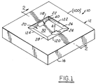
- Figure 1 is a perspective view of an embodiment in which the invention is used to advantage;
- Figure 2 is a cross-sectional view taken along lines 2-2 of Figure 1;
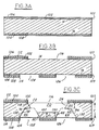
- Figures 3A through 3C illustrate various process steps in fabricating the embodiment illustrated in Figure 2; and
- Figure 4 is an expanded view of a portion of the embodiment illustrated in Figure 2.
- Referring first to Figure 1,
aperture assembly 10 is shown for the purposes of illustrating an example in which the invention is used to advantage.Aperture assembly 10 is here shown fabricated from a {100}silicon substrate 12 which has been sawed from a wafer, by conventional means, such that topplanar surface 14 and bottomplanar surface 16 lie substantially in the {100} nominal crystalline plane. Firstetchant pit 20 is shown formed through topplanar surface 14 withside walls bottom wall 30.Side walls aperture 40 andaperture 42 are symmetrically positioned insubstrate 12. - It is to be understood that although a {100} silicon substrate is shown, the invention may be used to advantage with substrates having major surfaces lying in other planar directions such as, for example, {110} silicon. In general, the invention may be used to advantage with any monocrystalline substrate.
- Referring now to Figure 2,
aperture 40 andaperture 42 are generally defined by the intersection of topetchant pit 20 with respective bottometchant pit 44 and bottometchant pit 46. As described in greater detail later herein with particular reference to Figures 3A through 3C, bottometchant pit 44 is defined byside walls top wall 56 lying in the {100} plane.Side walls planar surface 16 or the {100} planes in general. -
Aperture plane 62 ofaperture 42 is shown in Figure 2 as a plane betweenprotruding edges aperture 42. Protrudingedge 64 is defined by the intersection of topetchant pit 20 withtop wall 56 of bottometchant pit 44. Protrudingedge 66 is defined by the intersection of bottometchant pit 44 withbottom wall 30 of topetchant pit 20.Aperture axis 68 ofaperture 42 is shown perpendicular toaperture plane 62 midway betweenprotruding edges planar surface 16, or the {100} planes in general, is herein designated as angle β. -
Aperture 40 is shown in Figure 2 as being symmetrically formed insubstrate 12 with respect toaperture 42. Bottometchant pit 46 is havingtop wall 76 lying in the {100} plane andside walls 78, 80, 82 (not shown), and 84 (not shown) lying in the {111} planes.Side walls 78, 80, 82 and 84 are etched at an angle φ with respect to bottomplanar surface 16 or the {100} planes in general. -
Aperture plane 92 ofaperture 40 is defined as a planar surface betweenprotruding edges 94 and 96 ofaperture 40. Protrudingedge 96 is defined by the intersection of topetchant pit 20 withtop wall 76 of bottometchant pit 46. Protruding edge 94 is defined by the intersection of bottometchant pit 46 withbottom wall 30 of topetchant pit 20. Aperture axis 98 ofaperture 40 is shown perpendicular toaperture plane 92 midway between protrudingedges 94 and 96. The angle ofaperture plane 92 with respect to topplanar surface 14, or the {100} planes in general, is herein designated as angle β. - Referring now to Figures 3A through 3C, wherein like numerals refer to like parts shown in Figures 1 and 2, the fabrication of
aperture assembly 10 is now described. The fabrication steps described herein utilize photolithographic and etching techniques well known in the microelectronics industry.Substrate 12 is illustrated in Figure 3A as a silicon substrate, preferably having been sawed to a thickness of approximately 200 to 500 microns with major surfaces lying substantially in the {100} planes. Top and bottomsilicon oxide layers substrate 12 using conventional techniques well known in the semiconductor industry. Layer ofsilicon nitride 106 and layer ofsilicon nitride 108 are deposited over respectivesilicon oxide layers Silicon oxide layer 102 andsilicon nitride layer 106, together definepassivation layer 107. Similarly, the combination ofsilicon oxide layer 104 andsilicon nitride layer 108 definepassivation layer 109. - With particular reference to Figure 3B, photo-resist
layers respective passivation layers Rectangular etchant pattern 116 is delineated in photo-resistlayer 112 by conventional photolithographic techniques.Rectangular etchant pattern 116 is etched throughpassivation layer 107 thereby exposing a corresponding rectangular portion of topplanar surface 14 for etchingtop etchant pit 20 in a subsequent etching step. In a similar manner, bottomrectangular pattern 126 and bottomrectangular pattern 128 are delineated through bottom photo-resistlayer 114 andpassivation layer 109. - Referring now to Figure 3C, a wet anisotropic etchant solution such as aqueous-potassium-hydroxide solution or ethylene-diamine-pyrocatecol solution, is applied to top
rectangular pattern 116, bottomrectangular pattern 126, and bottomrectangular pattern 128 to form respectivetop etchant pit 20,bottom etchant pit 44 andbottom etchant pit 46. For the {100} silicon wafer illustrated herein, the wet etchant acts against the {100} planes at a rate approximately 100 times greater than against the {111} planes. The etchant steps are timed such thattop etchant pit 20 is etched against the {100} planes to a distance d₁ before bottomplanar surface 16. Stated another way,top etchant pit 20 is etched to a depth t-d₁ where t is the thickness ofsubstrate 12. During the etching of the planes to a distance of d₁, there will be relatively little etching against the {111} planes. Accordingly, sidewalls 22, 24, 26 (Figure 1) and 28 (Figure 1), which lie in the {111} planes, are slightly offset fromrectangular pattern 116. More specifically, the intersection ofsidewalls planar surface 14 defines, respectively, lefttransverse edge 118, righttransverse edge 120, longitudinal edge 122 (Figure 1), and longitudinal edge 124 (Figure 1) ofetchant pit 20, all of which are slightly offset fromrectangular pattern 116. - Both
bottom etchant pit 44 andbottom etchant pit 46 are etched to a depth d₂ before topplanar surface 14. That is,bottom etchant pit 44 andbottom etchant pit 46 are etched to a depth t-d₂. With respect tobottom etchant pit 44, the intersection ofsidewalls planar surface 16 defines, respectively, lefttransverse edge 130, righttransverse edge 132, longitudinal edge 134 (not shown), and longitudinal edge 136 (not shown), all of which are slightly offset fromrectangular pattern 126. Referring tobottom etchant pit 46, the intersection ofsidewalls 78, 80, 82 (not shown) and 84 (not shown) with bottomplanar surface 16 defines, respectively, lefttransverse edge 138, righttransverse edge 140, longitudinal edge 142 (not shown), and longitudinal edge 144 (not shown), all of which are slightly offset fromrectangular pattern 128. -
Top etchant pit 20 and bottom etchant pits 44 and 46 are here shown etched to the same depth (d₁=d₂) such that the etchant steps are performed concurrently. That is, by etching to the same depth, the timing of the etching steps is substantially the same thereby enabling the etching steps to be performed concurrently. - The trigonometric relationship of the various etching parameters described herein above with respect to the desired or preselected angle of the aperture plane is now described with reference to Figure 4. For clarity of illustration, the following description is with particular reference to
aperture 42. Those skilled in the art, however, will recognize that the description herein is also applicable toaperture 40, and is further applicable to other apertures desired by a designer which are not specifically illustrated herein. It is to be further noted that the description herein relates to a {100} silicon wafer. The teachings described, however, are applicable to other monocrystaline substrates such as, for example, {110} crystaline structures wherein the {111} planes intersect the planes at an angle of 90°. - As previously described herein with reference to Figure 2,
aperture plane 62 extends through protrudingedges planar surface 16.Side walls etchant pit 44 lie along the {111} planes at an angle φ to the nominal {100} plane of 54.7°. Preselected angle β is related to the longitudinal distance between lefttransverse edge 130 of bottom etchant pit and the opposing righttransverse edge 120 of top etchant pit 20 (ΔL), the preselected distance oftop etchant pit 20 from bottom planar surface 16 (d₁), the preselected distance ofbottom etchant pit 44 from top planar surface 14 (d₂), the angle between the {111} planes and the nominal {100} plane (φ) and the thickness of substrate 12 (t) by the following trigonometric relation:
Thus, it is seen that the preselected angle β may be changed by the designer by changing any of the parameters shown in the above equation. The designer is therefore able to select a desired aperture angle by simply selecting from: the type of monocrystaline substrate (φ); wafer thickness (t); longitudinal offset of opposing etchant pits (ΔL); and the etchant time or thickness (d₁ + d₂).
Claims (7)
- A method for anisotropically etching a first aperture into a monocrystalline substrate such that the plane of the first aperture is inclined at a selectable angle (β) with respect to the nominal crystalline planes of the substrate, said method comprising the steps of -:a) dimensioning said substrate of thickness (t) with top (14) and bottom (16) planar surfaces substantially parallel to said nominal crystalline planes;b) anisotropically etching a first etchant pit (20) through said top planar surface (14) and against said nominal crystalline planes to a first preselected distance (d₁) from said bottom planar surface (16), said first etchant pit (20) having plane surface sides (22, 24) along intersecting crystalline planes to said nominal crystalline planes, the intersection of said plane surface sides with said top planar surface defining an angle of intersection (φ), a first pair of longitudinal edges (122, 124) and a first pair of transverse edges (118, 120) of said first etchant pit (20), andc) anisotropically etching a second etchant pit (44) through said bottom planar surface (16) and against said nominal crystalline planes to a second preselected distance (d₂) from said top planar surface (14), whereby the areas of the first (20) and the second (44) etchant pits vertically overlap each other, the centre of the second etchant pit (44) being laterally offset from that of the first etchant pit (20) and the sum of said first and second preselected distances (d₁) and (d₂) is larger than the thickness (t) of said substrate so that a portion of said second etchant pit (44) intersects a portion of said first etchant pit (20) to form said first aperture (42), said second etchant pit (44) having plane surface sides (48, 50) along said intersecting crystalline planes, the intersection of said plane surface sides with said bottom planar surface (16) defining a second pair of longitudinal edges and a second pair of transverse edges (130, 132) of said second etchant pit (44), the plane of the first aperture (42) being defined as that plane which occurs between a first protruding edge (64), defined by the intersection of the first etchant pit (20) with the top wall (56) of the second etchant pit (44), and a second protruding edge (66), defined by the intersection of the second etchant pit (44) with the bottom wall (30) of the first etchant pit (20), one edge (130) of said second pair of transverse edges (130, 132) being longitudinally offset from an opposing one (120) of said first pair of transverse edges (118, 120) by a preselected longitudinal offset (ΔL), said opposing offset edges (130, 120) belonging to those intersecting crystalline planes which include said first and second protruding edges (64, 66), the angle of inclination (β) of the plane (62) of the aperture relative to the top and bottom planar surfaces (14, 16) being related to the longitudinal offset (ΔL), the thickness (t) of the substrate, the first preselected distance (d₁) of the first etchant pit (20) from the bottom planar surface (16), the second preselected distance (d₂) of the second etchant pit (44) from the top planar surface (14) and the angle of intersection (φ) between said intersecting planes and said nominal planes by the trigonometric relationship:

- A method as claimed in claim 1, wherein the intersection of said plane surface sides (22, 24) with said top planar surface (14) defines a rectangle having a left transverse edge (118), a right transverse edge (120) and said first pair of longitudinal edges (122, 124); and wherein the intersection of said plane surface sides (48, 50) with said bottom planar surface (16) defines a rectangle having a left transverse edge (130), a right transverse edge (132,) and said second pair of longitudinal edges.
- A method as claimed in claim 1 or 2, wherein said first preselected distance (d₁) of said first etchant pit (20) from said bottom planar surface (16) is substantially equal to said preselected distance (d₂) of said second etchant pit (44) from said first planar surface (14), said first and second etchant pits (20, 44) being concurrently formed in a single etchant step.
- A method as claimed in claim 2, for anisotropically etching a second aperture (40) into said substrate such that the plane of said second aperture is inclined at a selectable angle (beta) with respect to said nominal crystalline planes of said substrate, the method further comprising the step of anisotropically etching a third etchant pit (46) through said bottom planar surface (16) and against said nominal crystalline planes to said second preselected distance (d₂) from said top planar surface (14), a portion of said third etchant pit (46) intersecting a portion of said first etchant pit (20) to define said second aperture (40), symmetrically with respect to said first aperture (42).
- A method as claimed in any preceding claim, wherein said substrate comprises a silicon substrate.
- A method as claimed in any preceding claim, wherein said nominal crystalline planes comprise (100) planes and said intersecting crystalline planes comprise (111) planes and said angle of intersection (φ) is approximately 54.7°.
- A method as claimed in any one of claims 1 to 5, wherein said nominal crystalline planes comprise (110) planes and said intersecting crystalline planes comprise (111) planes and said angle of intersection (φ) is approximately 90°.
Applications Claiming Priority (2)
| Application Number | Priority Date | Filing Date | Title |
|---|---|---|---|
| US07/152,718 US4808260A (en) | 1988-02-05 | 1988-02-05 | Directional aperture etched in silicon |
| US152718 | 1988-02-05 |
Publications (3)
| Publication Number | Publication Date |
|---|---|
| EP0328281A2 EP0328281A2 (en) | 1989-08-16 |
| EP0328281A3 EP0328281A3 (en) | 1990-08-08 |
| EP0328281B1 true EP0328281B1 (en) | 1995-09-20 |
Family
ID=22544109
Family Applications (1)
| Application Number | Title | Priority Date | Filing Date |
|---|---|---|---|
| EP89300864A Expired - Lifetime EP0328281B1 (en) | 1988-02-05 | 1989-01-30 | Directable aperture etched in silicon |
Country Status (5)
| Country | Link |
|---|---|
| US (1) | US4808260A (en) |
| EP (1) | EP0328281B1 (en) |
| JP (1) | JPH01235239A (en) |
| CA (1) | CA1286423C (en) |
| DE (1) | DE68924285T2 (en) |
Families Citing this family (32)
| Publication number | Priority date | Publication date | Assignee | Title |
|---|---|---|---|---|
| US4907748A (en) * | 1988-08-12 | 1990-03-13 | Ford Motor Company | Fuel injector with silicon nozzle |
| DE4104019C1 (en) * | 1991-02-09 | 1992-04-23 | Robert Bosch Gmbh, 7000 Stuttgart, De | |
| US5317938A (en) * | 1992-01-16 | 1994-06-07 | Duke University | Method for making microstructural surgical instruments |
| US5920067A (en) * | 1992-03-13 | 1999-07-06 | The United States Of America As Represented By The Secretary Of Commerce | Monocrystalline test and reference structures, and use for calibrating instruments |
| DE4233703A1 (en) * | 1992-10-07 | 1994-04-14 | Bosch Gmbh Robert | Silicon@ injection plate mfr. - has both sides of bottom plate etched simultaneously with the use of etching masks |
| JP3333560B2 (en) * | 1992-10-23 | 2002-10-15 | リコーエレメックス株式会社 | Silicon substrate etching method |
| US5286002A (en) * | 1993-01-12 | 1994-02-15 | Siemens Automotive L.P. | Fuel injector having a composite silicon valve |
| US5308442A (en) * | 1993-01-25 | 1994-05-03 | Hewlett-Packard Company | Anisotropically etched ink fill slots in silicon |
| US5387314A (en) * | 1993-01-25 | 1995-02-07 | Hewlett-Packard Company | Fabrication of ink fill slots in thermal ink-jet printheads utilizing chemical micromachining |
| EP0611886B1 (en) * | 1993-02-17 | 1998-12-23 | Denso Corporation | Fluid injection nozzle |
| DE4318407A1 (en) * | 1993-06-03 | 1994-12-08 | Rossendorf Forschzent | Microcapillary with integrated chemical microsensors and process for their manufacture |
| US5383597A (en) * | 1993-08-06 | 1995-01-24 | Ford Motor Company | Apparatus and method for controlling the cone angle of an atomized spray from a low pressure fuel injector |
| WO1995004881A1 (en) * | 1993-08-06 | 1995-02-16 | Ford Motor Company | A fuel injector |
| US5956058A (en) * | 1993-11-05 | 1999-09-21 | Seiko Epson Corporation | Ink jet print head with improved spacer made from silicon single-crystal substrate |
| JPH07279796A (en) * | 1994-02-16 | 1995-10-27 | Nippondenso Co Ltd | Fluid injection nozzle and its manufacture |
| US5487483A (en) * | 1994-05-24 | 1996-01-30 | Xerox Corporation | Nozzles for ink jet devices and method for microfabrication of the nozzles |
| US5901425A (en) | 1996-08-27 | 1999-05-11 | Topaz Technologies Inc. | Inkjet print head apparatus |
| US6071426A (en) * | 1997-12-08 | 2000-06-06 | The Regents Of The University Of California | Micro benchtop optics by bulk silicon micromachining |
| JP3692826B2 (en) * | 1999-04-15 | 2005-09-07 | オムロン株式会社 | Semiconductor device |
| US6805432B1 (en) | 2001-07-31 | 2004-10-19 | Hewlett-Packard Development Company, L.P. | Fluid ejecting device with fluid feed slot |
| US7105097B2 (en) * | 2002-01-31 | 2006-09-12 | Hewlett-Packard Development Company, L.P. | Substrate and method of forming substrate for fluid ejection device |
| US7387742B2 (en) * | 2002-03-11 | 2008-06-17 | Becton, Dickinson And Company | Silicon blades for surgical and non-surgical use |
| BRPI0308319B1 (en) * | 2002-03-11 | 2015-06-09 | Beaver Visitec Int Us Inc | Method for making a crystalline material cutting device and method for making a surgical blade of crystalline material |
| US20090007436A1 (en) * | 2003-03-10 | 2009-01-08 | Daskal Vadim M | Silicon blades for surgical and non-surgical use |
| US20050155955A1 (en) * | 2003-03-10 | 2005-07-21 | Daskal Vadim M. | Method for reducing glare and creating matte finish of controlled density on a silicon surface |
| US20040181950A1 (en) * | 2003-03-17 | 2004-09-23 | Rodgers Murray Steven | Alignment of microkeratome blade to blade handle |
| US7785485B2 (en) * | 2003-09-17 | 2010-08-31 | Becton, Dickinson And Company | System and method for creating linear and non-linear trenches in silicon and other crystalline materials with a router |
| US7396484B2 (en) * | 2004-04-30 | 2008-07-08 | Becton, Dickinson And Company | Methods of fabricating complex blade geometries from silicon wafers and strengthening blade geometries |
| JP5448581B2 (en) * | 2008-06-19 | 2014-03-19 | キヤノン株式会社 | Method for manufacturing substrate for liquid discharge head and method for processing substrate |
| US8729591B2 (en) * | 2009-02-13 | 2014-05-20 | Tsmc Solid State Lighting Ltd. | Opto-electronic device package with a semiconductor-based sub-mount having SMD metal contacts |
| JP5991179B2 (en) * | 2012-12-10 | 2016-09-14 | セイコーエプソン株式会社 | Liquid ejecting head and liquid ejecting apparatus |
| JP2023108679A (en) * | 2022-01-26 | 2023-08-07 | キヤノン株式会社 | Recording element substrate and manufacturing method thereof |
Citations (2)
| Publication number | Priority date | Publication date | Assignee | Title |
|---|---|---|---|---|
| EP0075102A2 (en) * | 1981-09-22 | 1983-03-30 | Siemens Aktiengesellschaft | Thyristor with a multi-layer PNPN semiconductor body and process for its manufacture |
| WO1985003165A1 (en) * | 1984-01-06 | 1985-07-18 | Aine Harry R | Method of undercut anisotropic etching of semiconductor material |
Family Cites Families (10)
| Publication number | Priority date | Publication date | Assignee | Title |
|---|---|---|---|---|
| US3977071A (en) * | 1969-09-29 | 1976-08-31 | Texas Instruments Incorporated | High depth-to-width ratio etching process for monocrystalline germanium semiconductor materials |
| US3888708A (en) * | 1972-02-17 | 1975-06-10 | Kensall D Wise | Method for forming regions of predetermined thickness in silicon |
| US4169008A (en) * | 1977-06-13 | 1979-09-25 | International Business Machines Corporation | Process for producing uniform nozzle orifices in silicon wafers |
| JPS5562732A (en) * | 1978-11-06 | 1980-05-12 | Chiyou Lsi Gijutsu Kenkyu Kumiai | Preparation of aperture stop |
| US4514896A (en) * | 1981-03-25 | 1985-05-07 | At&T Bell Laboratories | Method of forming current confinement channels in semiconductor devices |
| US4733823A (en) * | 1984-10-15 | 1988-03-29 | At&T Teletype Corporation | Silicon nozzle structures and method of manufacture |
| US4628576A (en) * | 1985-02-21 | 1986-12-16 | Ford Motor Company | Method for fabricating a silicon valve |
| US4647013A (en) * | 1985-02-21 | 1987-03-03 | Ford Motor Company | Silicon valve |
| US4758368A (en) * | 1986-07-21 | 1988-07-19 | Motorola Inc. | Method for etching silicon wafers using a potassium hydroxide and water etching solution |
| US4765864A (en) * | 1987-07-15 | 1988-08-23 | Sri International | Etching method for producing an electrochemical cell in a crystalline substrate |
-
1988
- 1988-02-05 US US07/152,718 patent/US4808260A/en not_active Expired - Fee Related
-
1989
- 1989-01-16 CA CA000588364A patent/CA1286423C/en not_active Expired - Lifetime
- 1989-01-30 EP EP89300864A patent/EP0328281B1/en not_active Expired - Lifetime
- 1989-01-30 DE DE68924285T patent/DE68924285T2/en not_active Expired - Fee Related
- 1989-02-03 JP JP1024088A patent/JPH01235239A/en active Pending
Patent Citations (2)
| Publication number | Priority date | Publication date | Assignee | Title |
|---|---|---|---|---|
| EP0075102A2 (en) * | 1981-09-22 | 1983-03-30 | Siemens Aktiengesellschaft | Thyristor with a multi-layer PNPN semiconductor body and process for its manufacture |
| WO1985003165A1 (en) * | 1984-01-06 | 1985-07-18 | Aine Harry R | Method of undercut anisotropic etching of semiconductor material |
Also Published As
| Publication number | Publication date |
|---|---|
| CA1286423C (en) | 1991-07-16 |
| US4808260A (en) | 1989-02-28 |
| JPH01235239A (en) | 1989-09-20 |
| EP0328281A2 (en) | 1989-08-16 |
| EP0328281A3 (en) | 1990-08-08 |
| DE68924285D1 (en) | 1995-10-26 |
| DE68924285T2 (en) | 1996-02-29 |
Similar Documents
| Publication | Publication Date | Title |
|---|---|---|
| US4808260A (en) | Directional aperture etched in silicon | |
| US4863560A (en) | Fabrication of silicon structures by single side, multiple step etching process | |
| US4961821A (en) | Ode through holes and butt edges without edge dicing | |
| DE68918982T2 (en) | Method for separating integrated circuits on a substrate. | |
| US5128282A (en) | Process for separating image sensor dies and the like from a wafer that minimizes silicon waste | |
| US5196378A (en) | Method of fabricating an integrated circuit having active regions near a die edge | |
| US4542397A (en) | Self aligning small scale integrated circuit semiconductor chips to form large area arrays | |
| US4814296A (en) | Method of fabricating image sensor dies for use in assembling arrays | |
| EP0212219B1 (en) | Visibility enhancement of first order alignment marks | |
| US5219796A (en) | Method of fabricating image sensor dies and the like for use in assembling arrays | |
| US5484507A (en) | Self compensating process for aligning an aperture with crystal planes in a substrate | |
| US5277755A (en) | Fabrication of three dimensional silicon devices by single side, two-step etching process | |
| US5282926A (en) | Method of anisotropically etching monocrystalline, disk-shaped wafers | |
| EP1569265A3 (en) | Semiconductor device having trenches and method of forming trenches | |
| US5338400A (en) | Micromachining process for making perfect exterior corner in an etchable substrate | |
| US4309813A (en) | Mask alignment scheme for laterally and totally dielectrically isolated integrated circuits | |
| EP0597302A2 (en) | Etching method for silicon substrate | |
| US6033489A (en) | Semiconductor substrate and method of making same | |
| US20040121560A1 (en) | Silicon wafer break pattern, silicon substrate, and method of generating silicon wafer break pattern | |
| US5827756A (en) | Method of manufacturing semiconductor device | |
| JPS63299144A (en) | Method of separating interface sealed by oxide protective layer for pad | |
| US4269653A (en) | Aperture stop | |
| US5399901A (en) | Semiconductor devices having a mesa structure and method of fabrication for improved surface voltage breakdown characteristics | |
| US5273807A (en) | Substrate having a V-shaped groove of a special configuration in a substrate | |
| EP0402482A1 (en) | Method of forming pattern |
Legal Events
| Date | Code | Title | Description |
|---|---|---|---|
| PUAI | Public reference made under article 153(3) epc to a published international application that has entered the european phase |
Free format text: ORIGINAL CODE: 0009012 |
|
| AK | Designated contracting states |
Kind code of ref document: A2 Designated state(s): DE FR GB |
|
| PUAL | Search report despatched |
Free format text: ORIGINAL CODE: 0009013 |
|
| AK | Designated contracting states |
Kind code of ref document: A3 Designated state(s): DE FR GB |
|
| 17P | Request for examination filed |
Effective date: 19901221 |
|
| 17Q | First examination report despatched |
Effective date: 19920106 |
|
| GRAA | (expected) grant |
Free format text: ORIGINAL CODE: 0009210 |
|
| AK | Designated contracting states |
Kind code of ref document: B1 Designated state(s): DE FR GB |
|
| PG25 | Lapsed in a contracting state [announced via postgrant information from national office to epo] |
Ref country code: FR Effective date: 19950920 |
|
| REF | Corresponds to: |
Ref document number: 68924285 Country of ref document: DE Date of ref document: 19951026 |
|
| EN | Fr: translation not filed | ||
| PLBE | No opposition filed within time limit |
Free format text: ORIGINAL CODE: 0009261 |
|
| STAA | Information on the status of an ep patent application or granted ep patent |
Free format text: STATUS: NO OPPOSITION FILED WITHIN TIME LIMIT |
|
| 26N | No opposition filed | ||
| REG | Reference to a national code |
Ref country code: GB Ref legal event code: 746 Effective date: 19961206 |
|
| PGFP | Annual fee paid to national office [announced via postgrant information from national office to epo] |
Ref country code: GB Payment date: 19971222 Year of fee payment: 10 |
|
| PGFP | Annual fee paid to national office [announced via postgrant information from national office to epo] |
Ref country code: DE Payment date: 19980123 Year of fee payment: 10 |
|
| PG25 | Lapsed in a contracting state [announced via postgrant information from national office to epo] |
Ref country code: GB Free format text: LAPSE BECAUSE OF NON-PAYMENT OF DUE FEES Effective date: 19990130 |
|
| GBPC | Gb: european patent ceased through non-payment of renewal fee |
Effective date: 19990130 |
|
| PG25 | Lapsed in a contracting state [announced via postgrant information from national office to epo] |
Ref country code: DE Free format text: LAPSE BECAUSE OF NON-PAYMENT OF DUE FEES Effective date: 19991103 |