EP0326749B1 - Magneto-resistive sensor element - Google Patents
Magneto-resistive sensor element Download PDFInfo
- Publication number
- EP0326749B1 EP0326749B1 EP88311028A EP88311028A EP0326749B1 EP 0326749 B1 EP0326749 B1 EP 0326749B1 EP 88311028 A EP88311028 A EP 88311028A EP 88311028 A EP88311028 A EP 88311028A EP 0326749 B1 EP0326749 B1 EP 0326749B1
- Authority
- EP
- European Patent Office
- Prior art keywords
- sensor element
- magneto
- central
- sides
- region
- Prior art date
- Legal status (The legal status is an assumption and is not a legal conclusion. Google has not performed a legal analysis and makes no representation as to the accuracy of the status listed.)
- Expired - Lifetime
Links
- 230000007704 transition Effects 0.000 claims description 15
- 210000003739 neck Anatomy 0.000 description 9
- 230000005381 magnetic domain Effects 0.000 description 7
- 239000000463 material Substances 0.000 description 3
- 238000010276 construction Methods 0.000 description 2
- 238000000034 method Methods 0.000 description 2
- 230000005330 Barkhausen effect Effects 0.000 description 1
- 229910001030 Iron–nickel alloy Inorganic materials 0.000 description 1
- 230000002411 adverse Effects 0.000 description 1
- 239000004020 conductor Substances 0.000 description 1
- 238000010348 incorporation Methods 0.000 description 1
- 238000004519 manufacturing process Methods 0.000 description 1
- 229920006395 saturated elastomer Polymers 0.000 description 1
- 238000007493 shaping process Methods 0.000 description 1
Images
Classifications
-
- G—PHYSICS
- G11—INFORMATION STORAGE
- G11B—INFORMATION STORAGE BASED ON RELATIVE MOVEMENT BETWEEN RECORD CARRIER AND TRANSDUCER
- G11B5/00—Recording by magnetisation or demagnetisation of a record carrier; Reproducing by magnetic means; Record carriers therefor
- G11B5/127—Structure or manufacture of heads, e.g. inductive
- G11B5/33—Structure or manufacture of flux-sensitive heads, i.e. for reproduction only; Combination of such heads with means for recording or erasing only
- G11B5/39—Structure or manufacture of flux-sensitive heads, i.e. for reproduction only; Combination of such heads with means for recording or erasing only using magneto-resistive devices or effects
- G11B5/3903—Structure or manufacture of flux-sensitive heads, i.e. for reproduction only; Combination of such heads with means for recording or erasing only using magneto-resistive devices or effects using magnetic thin film layers or their effects, the films being part of integrated structures
- G11B5/398—Specially shaped layers
-
- G—PHYSICS
- G01—MEASURING; TESTING
- G01R—MEASURING ELECTRIC VARIABLES; MEASURING MAGNETIC VARIABLES
- G01R33/00—Arrangements or instruments for measuring magnetic variables
- G01R33/02—Measuring direction or magnitude of magnetic fields or magnetic flux
- G01R33/06—Measuring direction or magnitude of magnetic fields or magnetic flux using galvano-magnetic devices
- G01R33/09—Magnetoresistive devices
-
- G—PHYSICS
- G11—INFORMATION STORAGE
- G11B—INFORMATION STORAGE BASED ON RELATIVE MOVEMENT BETWEEN RECORD CARRIER AND TRANSDUCER
- G11B5/00—Recording by magnetisation or demagnetisation of a record carrier; Reproducing by magnetic means; Record carriers therefor
- G11B5/127—Structure or manufacture of heads, e.g. inductive
- G11B5/33—Structure or manufacture of flux-sensitive heads, i.e. for reproduction only; Combination of such heads with means for recording or erasing only
- G11B5/39—Structure or manufacture of flux-sensitive heads, i.e. for reproduction only; Combination of such heads with means for recording or erasing only using magneto-resistive devices or effects
- G11B5/3903—Structure or manufacture of flux-sensitive heads, i.e. for reproduction only; Combination of such heads with means for recording or erasing only using magneto-resistive devices or effects using magnetic thin film layers or their effects, the films being part of integrated structures
Definitions
- the present invention seeks to provide a magnetoresistive sensor element which has a stable central single magnetic domain which re-establishes itself even after a central region has been saturated in the direction of the hard axis of magnetisation, and is maintained irrespective of photo-lithic processes used in the manufacture of the sensor element.
- conductors for sensing the change in resistivity of the sensor element under the influence of an external magnetic field are provided as shown, for example, in Figure 5 of US-A-4,556,925 or Figure 12 of EP-A-0,279,537.
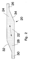
- Figure 2 shows another embodiment of a magneto-resistive sensor element 20 according to the present invention.
- This embodiment is not symmetrical about a centre line. Rather, on one side, a first neck 30 occurs on the lower (as shown in Figure 2) half of the sensor element and a neck 26 occurs on the upper half of the sensor element.
- transition regions 24,28 are skewed relative to one another.
- the sensor element has a relatively wide central region 22 with opposed parallel sides.
- the transition regions 24,28 are skewed relative to one another with a respective inclined side 34,32 leading to the respective necks 26,30. If the necks 26,30 are arranged so that one side is flush with a side of the central region 22, as shown in Figure 2, then the respective transition regions 24,28 include only one inclined side, 34 or 32 respectively.
- the transition regions 24,28 will have two inclined sides as in the embodiment shown in Figure 1.
- the easy axis of magnetisation shown by the arrow in Figure 2 may or may not be skewed relative to the parallel sides of the central region.
Landscapes
- Engineering & Computer Science (AREA)
- Manufacturing & Machinery (AREA)
- Physics & Mathematics (AREA)
- Condensed Matter Physics & Semiconductors (AREA)
- General Physics & Mathematics (AREA)
- Measuring Magnetic Variables (AREA)
- Hall/Mr Elements (AREA)
- Magnetic Heads (AREA)
Description
- This invention relates to magneto-resistive sensor elements, for example, for incorporation into magneto-resistive heads.
- The output of a magneto-resistive sensor element is adversely affected by multiple magnetic domains in a sense region, because the walls of the magnetic domain suddenly move under influence of the magnetic fields being sensed. This sudden movement of the domain walls causes an uneven response in the output of the sensor element, limiting its usefulness. Efforts have been made to provide a single magnetic domain in the sense region during sensor "read" operations to avoid Barkhausen noise. Among these efforts have been efforts to shape the sensor element in such a manner that there is a single magnetic domain in the sense region.
- One example of such shaping is the so-called football-shaped sensor element (US-A-4,556,925 and EP-A-0,279,537, this European Patent Application having been published on 24.8.88 and therefore falling under Article 54(3) EPC). The football-shaped sensor element has a highly stable central single magnetic domain. However, experience has shown that even this sensor element can be fractured into two horizontal domains under the influence of high external magnetic fields (such as one may find if the sensor element is incorporated into a read/write head) which drives the sensor element into saturation of the hard axis of magnetisation. Further, routine photo-lithic process variations can significantly blunt the end points of the football-shape, thereby eliminating the very geometry which stabilised the central single magnetic domain.
- The present invention seeks to provide a magnetoresistive sensor element which has a stable central single magnetic domain which re-establishes itself even after a central region has been saturated in the direction of the hard axis of magnetisation, and is maintained irrespective of photo-lithic processes used in the manufacture of the sensor element.
- According to one aspect of the present invention, there is provided a magneto-resistive sensor element which has a central region (12;22), said central region being relatively wide compared to neck regions (16;26,30) and a transition region (14;24,28) between each neck region and the central region, said neck regions having sides substantially parallel to the sides of said central region.
- In one embodiment, the magneto-resistive sensor element is symmetrical about a centre line. In another embodiment the transition regions are skewed relative to a centre line.
- Preferably the transition regions each have at least one side inclined to the opposed parallel sides of the central region. In one embodiment, an easy axis of magnetisation is oriented in a direction parallel to the opposed parallel sides of the central region. In another embodiment, an easy axis of magnetisation is oriented in a direction at an angle to the opposed parallel sides of the central portion.
- According to another aspect of the present invention, there is provided a bottleneck magneto-resistive element which has a central wide portion (12;22) with two ends, a narrowing transition portion (14;24,28) connected to each end with at least one inclined side (32,34), and a bottleneck portion (16;26,30) connected to each transition portion, the bottleneck portion having a width less than the central wide portion and being substantially rectangular in shape with the sides of the rectangle's long dimension being substantially parallel with the opposed parallel sides of said central region.
- The invention is illustrated, merely by way of example, in the accompanying drawings, in which:-
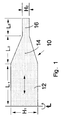
- Figure 1 is a partial plan view of one embodiment of a magneto-resistive sensor element according to the present invention; and
- Figure 2 is a plan view of another embodiment of a magneto-resistive sensor element according to the present invention.
- Referring first to Figure 1, there is shown one embodiment of a magneto-
resistive sensor element 10 according to the present invention. The sensor element is planar and is symmetrical about a centre line CL. The sensor element is also symmetrical or substantially symmetrical (as shown) about a centre line extending in the length direction. The half of the sensor element shown in Figure 1 comprises three regions, namely, a relatively widecentral region 12 with opposed parallel sides, atransition region 14 with inwardly inclined sides, and a relativelynarrow neck region 16 of generally rectangular shape. - The preferred material for the magneto-resistive sensor element is nominally 18:20 nickel-iron alloy. However, it may be constructed from any appropriate magneto-resistive material. The easy axis of magnetisation of the material of the sensor element is normally oriented along the axis or length direction of the sensor element 10 (parallel to the sides of the
central region 12 as indicated by the arrow in Figure 1), but may be skewed slightly as in the embodiment shown in Figure 2. That is, the easy axis of magnetisation in both embodiments may be parallel or skewed, depending upon the application for the sensor element; skewing slightly linearises the output of a magneto-resistive head employing the sensor element. - The following are experimentally derived parameters for the lengths and heights of the three
regions PARAMETER RANGE (µm) PRACTICAL LIMITS (µm) H₁ 2 - 15 4 - 10 H₂ 1 - 3 1 - 3 L₁ 0 - ∞ 5 - 50 L₂ 10 - ∞ 15 - 25 L₃ 5 - 25 10 - 20 THICKNESS 50 - 1000 A° 150 - 700 A° - It will be appreciated that conductors (not shown) for sensing the change in resistivity of the sensor element under the influence of an external magnetic field are provided as shown, for example, in Figure 5 of US-A-4,556,925 or Figure 12 of EP-A-0,279,537.
- Figure 2 shows another embodiment of a magneto-
resistive sensor element 20 according to the present invention. This embodiment is not symmetrical about a centre line. Rather, on one side, afirst neck 30 occurs on the lower (as shown in Figure 2) half of the sensor element and aneck 26 occurs on the upper half of the sensor element. Essentially,transition regions central region 22 with opposed parallel sides. Thetransition regions inclined side respective necks necks central region 22, as shown in Figure 2, then therespective transition regions transition regions
Claims (8)
- A magneto-resistive sensor element which has a central region (12;22), said central region being relatively wide compared to neck regions (16;26,30) and a transition region (14;24,28) between each neck region and the central region, said neck regions having sides substantially parallel to the sides of said central region.
- A magneto-resistive sensor element as claimed in claim 1, wherein the transition regions (14;24,28) each have at least one side (32,34) inclined to the opposed parallel sides of the central region (12;22).
- A magneto-resistive sensor element as claimed in claim 1 wherein both the transition regions (24,28) are skewed relative to a centre line substantially parallel with the parallel sides of said central wide region (12;22).
- A magneto-resistive sensor element as claimed in claim 1 and 2, which is symmetrical about a centre line which is substantially parallel with the parallel sides of said central wide region (12;22).
- A magneto-resistive sensor element as claimed in claim 4 wherein an easy axis of magnetisation is oriented in a direction parallel to the opposed parallel sides of the central region (12).
- A magneto-resistive sensor element as claimed in claim 1 or 2 wherein an easy axis of magnetisation is oriented in a direction at an angle to the opposed parallel sides of the central portion (22).
- A bottleneck magneto-resistive element which has a central wide portion (12;22) with two ends, a narrowing transition portion (14;24,28) connected to each said end with at least one inclined side (32, 34), and a bottleneck portion (16;26,30) connected to each transition portion, the bottleneck portion having a width less than the central wide portion and being substantially rectangular in shape with the sides of the rectangle's long dimension being substantially parallel with the opposed parallel sides of said central region.
- A magneto-resistive element as claimed in claim 7 wherein the shape is symmetrical about a centre line substantially parallel with the parallel sides of said central wide portion (12;22).
Applications Claiming Priority (2)
| Application Number | Priority Date | Filing Date | Title |
|---|---|---|---|
| US152792 | 1988-02-05 | ||
| US07/152,792 US4821133A (en) | 1987-02-17 | 1988-02-05 | Bottleneck magnetoresistive element |
Publications (3)
| Publication Number | Publication Date |
|---|---|
| EP0326749A2 EP0326749A2 (en) | 1989-08-09 |
| EP0326749A3 EP0326749A3 (en) | 1991-02-06 |
| EP0326749B1 true EP0326749B1 (en) | 1994-03-09 |
Family
ID=22544465
Family Applications (1)
| Application Number | Title | Priority Date | Filing Date |
|---|---|---|---|
| EP88311028A Expired - Lifetime EP0326749B1 (en) | 1988-02-05 | 1988-11-22 | Magneto-resistive sensor element |
Country Status (5)
| Country | Link |
|---|---|
| US (1) | US4821133A (en) |
| EP (1) | EP0326749B1 (en) |
| JP (1) | JPH0770762B2 (en) |
| CA (1) | CA1316596C (en) |
| DE (1) | DE3888342T2 (en) |
Cited By (1)
| Publication number | Priority date | Publication date | Assignee | Title |
|---|---|---|---|---|
| KR100780130B1 (en) | 2002-03-29 | 2007-11-27 | 가부시끼가이샤 도시바 | Magnetoresistive element and magnetic memory |
Families Citing this family (18)
| Publication number | Priority date | Publication date | Assignee | Title |
|---|---|---|---|---|
| US4956736A (en) * | 1988-12-16 | 1990-09-11 | Eastman Kodak Company | Thin film magnetic element having a rhombic shape |
| US5170303A (en) * | 1990-04-30 | 1992-12-08 | Seagate Technology Inc. | Inductive thin film head having improved readback characteristics |
| US5065094A (en) * | 1990-08-07 | 1991-11-12 | Seagate Technology, Inc. | Two terminal magnetoresistive sensor having DC blocking capacitor |
| US5208715A (en) * | 1990-08-31 | 1993-05-04 | Seagate Technology, Inc. | Shield geometry for stabilizing magnetic domain structure in a magnetoresistive head |
| EP0585008B1 (en) * | 1992-08-25 | 2000-11-15 | Seagate Technology LLC | A magnetoresistive sensor and method of making the same |
| WO1994027288A1 (en) * | 1993-05-11 | 1994-11-24 | Philips Electronics N.V. | Magnetoresistive element having composite structure and thin film magnetic head incorporating same |
| US5452166A (en) * | 1993-10-01 | 1995-09-19 | Applied Magnetics Corporation | Thin film magnetic recording head for minimizing undershoots and a method for manufacturing the same |
| TW349690U (en) * | 1994-12-16 | 1999-01-01 | Ibm | Magnetoresistive head with a magnetoresistive film shaped to provide an improved read sensitivity profile |
| JP2870437B2 (en) * | 1994-12-29 | 1999-03-17 | ヤマハ株式会社 | MR head and method of manufacturing the same |
| US6222702B1 (en) | 1997-08-15 | 2001-04-24 | Seagate Technology, Inc. | Magnetic read element shield having dimensions that minimize domain wall movement |
| US6222361B1 (en) * | 1997-12-04 | 2001-04-24 | Sony Precision Technology Inc. | Position detecting device using varying width magneto-resistive effect sensor |
| US6169646B1 (en) | 1998-11-18 | 2001-01-02 | Seagate Technology, Inc. | Magnetoresistive shield incorporating seedlayer for anisotropy enhancement |
| US6097578A (en) * | 1998-12-02 | 2000-08-01 | Seagate Technology, Inc. | Bottom shield design for magnetic read heads |
| US7123768B2 (en) * | 2000-04-26 | 2006-10-17 | Minolta Co., Ltd. | Apparatus and method for detecting a pattern |
| JP2010093277A (en) * | 2002-06-25 | 2010-04-22 | Renesas Technology Corp | Semiconductor integrated circuit device |
| US7168081B2 (en) * | 2003-08-29 | 2007-01-23 | Imation Corp. | Domain stabilized magneto-optic head |
| JP6186252B2 (en) * | 2013-11-13 | 2017-08-23 | アルプス電気株式会社 | Magnetic sensor |
| WO2018116783A1 (en) * | 2016-12-21 | 2018-06-28 | 株式会社村田製作所 | Magnetic sensor |
Family Cites Families (3)
| Publication number | Priority date | Publication date | Assignee | Title |
|---|---|---|---|---|
| JPS5845619A (en) * | 1981-09-09 | 1983-03-16 | Hitachi Ltd | Magneto-resistance effect type thin film magnetic head |
| US4535375A (en) * | 1983-01-14 | 1985-08-13 | Magnetic Peripherals, Inc. | Magnetoresistive head |
| US4731757A (en) * | 1986-06-27 | 1988-03-15 | Honeywell Inc. | Magnetoresistive memory including thin film storage cells having tapered ends |
-
1988
- 1988-02-05 US US07/152,792 patent/US4821133A/en not_active Expired - Lifetime
- 1988-09-01 JP JP63216473A patent/JPH0770762B2/en not_active Expired - Lifetime
- 1988-09-27 CA CA000578558A patent/CA1316596C/en not_active Expired - Fee Related
- 1988-11-22 DE DE3888342T patent/DE3888342T2/en not_active Expired - Fee Related
- 1988-11-22 EP EP88311028A patent/EP0326749B1/en not_active Expired - Lifetime
Cited By (1)
| Publication number | Priority date | Publication date | Assignee | Title |
|---|---|---|---|---|
| KR100780130B1 (en) | 2002-03-29 | 2007-11-27 | 가부시끼가이샤 도시바 | Magnetoresistive element and magnetic memory |
Also Published As
| Publication number | Publication date |
|---|---|
| JPH01208883A (en) | 1989-08-22 |
| DE3888342D1 (en) | 1994-04-14 |
| EP0326749A3 (en) | 1991-02-06 |
| US4821133A (en) | 1989-04-11 |
| DE3888342T2 (en) | 1994-06-16 |
| CA1316596C (en) | 1993-04-20 |
| EP0326749A2 (en) | 1989-08-09 |
| JPH0770762B2 (en) | 1995-07-31 |
Similar Documents
| Publication | Publication Date | Title |
|---|---|---|
| EP0326749A2 (en) | Magneto-resistive sensor element | |
| US7978441B2 (en) | CPP with elongated pinned layer | |
| US8659855B2 (en) | Trilayer reader with current constraint at the ABS | |
| DE69835410T2 (en) | Magnetoresistive read head with shielded magnetic tunnel junction | |
| US8018690B2 (en) | CPP magnetic recording head with self-stabilizing vortex configuration | |
| JP2866608B2 (en) | Yoke type spin valve MR read head | |
| JPH0439738B2 (en) | ||
| DE69317467T2 (en) | Arrangement of conductors for magnetoresistive transducers | |
| JPH01119913A (en) | Magnetic reading converter | |
| JPS63117310A (en) | Magnetic reluctivity reader/converter | |
| EP0449961B1 (en) | Permanent magnet shaped to provide uniform biasing of a magnetoresistive reproduce head | |
| EP0452369B1 (en) | Deposited permanent magnet for hard and easy axes biasing of a magnetoresistive head | |
| JPH02292708A (en) | Static reading magnetic head | |
| US5847904A (en) | Magnetoresistive device incorporating conductor geometry providing substantially uniform current flow for improved magnetic stability | |
| US6426853B1 (en) | Magnetoresistive effect sensor, thin-film magnetic head and thin-film wafer with the thin-film magnetic heads | |
| DE19738361A1 (en) | Magnetic detector to monitor rotation and movement of magnetic body | |
| US20030214765A1 (en) | Magnetoresistive read sensor with short permanent magnets | |
| WO1998049676A1 (en) | Dual layer magnetic exchange stabilization for mr heads | |
| EP0573149B1 (en) | Improved magnetoresistive transducer | |
| US5946169A (en) | Soft adjacent layer vertically biased magnetoresistive sensor having improved sensor stability | |
| EP0455359A2 (en) | Thin film magnetic head and method of manufacture thereof | |
| US6922884B2 (en) | Method for preventing magnetic damage to a GMR head during back-end processing | |
| EP0676747A2 (en) | Magnetoresistive transducer having insulating oxide exchange layer | |
| JPH01133213A (en) | Yoke type thin film magnetic head | |
| Brug et al. | Effect of sense current on Barkhausen noise in magnetoresistive recording heads |
Legal Events
| Date | Code | Title | Description |
|---|---|---|---|
| PUAI | Public reference made under article 153(3) epc to a published international application that has entered the european phase |
Free format text: ORIGINAL CODE: 0009012 |
|
| AK | Designated contracting states |
Kind code of ref document: A2 Designated state(s): DE FR GB |
|
| PUAL | Search report despatched |
Free format text: ORIGINAL CODE: 0009013 |
|
| RAP1 | Party data changed (applicant data changed or rights of an application transferred) |
Owner name: SEAGATE TECHNOLOGY INTERNATIONAL |
|
| AK | Designated contracting states |
Kind code of ref document: A3 Designated state(s): DE FR GB |
|
| 17P | Request for examination filed |
Effective date: 19910521 |
|
| 17Q | First examination report despatched |
Effective date: 19921218 |
|
| GRAA | (expected) grant |
Free format text: ORIGINAL CODE: 0009210 |
|
| AK | Designated contracting states |
Kind code of ref document: B1 Designated state(s): DE FR GB |
|
| REF | Corresponds to: |
Ref document number: 3888342 Country of ref document: DE Date of ref document: 19940414 |
|
| ET | Fr: translation filed | ||
| PLBE | No opposition filed within time limit |
Free format text: ORIGINAL CODE: 0009261 |
|
| STAA | Information on the status of an ep patent application or granted ep patent |
Free format text: STATUS: NO OPPOSITION FILED WITHIN TIME LIMIT |
|
| 26N | No opposition filed | ||
| PGFP | Annual fee paid to national office [announced via postgrant information from national office to epo] |
Ref country code: FR Payment date: 19961023 Year of fee payment: 9 |
|
| PG25 | Lapsed in a contracting state [announced via postgrant information from national office to epo] |
Ref country code: FR Free format text: THE PATENT HAS BEEN ANNULLED BY A DECISION OF A NATIONAL AUTHORITY Effective date: 19971130 |
|
| REG | Reference to a national code |
Ref country code: FR Ref legal event code: ST |
|
| REG | Reference to a national code |
Ref country code: GB Ref legal event code: 732E |
|
| REG | Reference to a national code |
Ref country code: GB Ref legal event code: IF02 |
|
| PGFP | Annual fee paid to national office [announced via postgrant information from national office to epo] |
Ref country code: GB Payment date: 20031103 Year of fee payment: 16 |
|
| PGFP | Annual fee paid to national office [announced via postgrant information from national office to epo] |
Ref country code: DE Payment date: 20031127 Year of fee payment: 16 |
|
| PG25 | Lapsed in a contracting state [announced via postgrant information from national office to epo] |
Ref country code: GB Free format text: LAPSE BECAUSE OF NON-PAYMENT OF DUE FEES Effective date: 20041122 |
|
| PG25 | Lapsed in a contracting state [announced via postgrant information from national office to epo] |
Ref country code: DE Free format text: LAPSE BECAUSE OF NON-PAYMENT OF DUE FEES Effective date: 20050601 |
|
| GBPC | Gb: european patent ceased through non-payment of renewal fee |
Effective date: 20041122 |