EP0321998A1 - Serial memory, picture memory device and reproduction apparatus comprising one or more serial memories - Google Patents
Serial memory, picture memory device and reproduction apparatus comprising one or more serial memories Download PDFInfo
- Publication number
- EP0321998A1 EP0321998A1 EP88202469A EP88202469A EP0321998A1 EP 0321998 A1 EP0321998 A1 EP 0321998A1 EP 88202469 A EP88202469 A EP 88202469A EP 88202469 A EP88202469 A EP 88202469A EP 0321998 A1 EP0321998 A1 EP 0321998A1
- Authority
- EP
- European Patent Office
- Prior art keywords
- address
- serial
- input means
- memory
- preset
- Prior art date
- Legal status (The legal status is an assumption and is not a legal conclusion. Google has not performed a legal analysis and makes no representation as to the accuracy of the status listed.)
- Granted
Links
- 230000015654 memory Effects 0.000 title claims abstract description 37
- 230000006870 function Effects 0.000 claims description 5
- 238000001514 detection method Methods 0.000 claims description 3
- 230000004913 activation Effects 0.000 claims description 2
- 238000007689 inspection Methods 0.000 claims description 2
- 238000010586 diagram Methods 0.000 description 8
- 230000007246 mechanism Effects 0.000 description 6
- 230000003213 activating effect Effects 0.000 description 1
- 230000008901 benefit Effects 0.000 description 1
- 230000008878 coupling Effects 0.000 description 1
- 238000010168 coupling process Methods 0.000 description 1
- 238000005859 coupling reaction Methods 0.000 description 1
- 238000005516 engineering process Methods 0.000 description 1
- 230000004044 response Effects 0.000 description 1
- 230000033764 rhythmic process Effects 0.000 description 1
- 230000001360 synchronised effect Effects 0.000 description 1
- 230000007704 transition Effects 0.000 description 1
Images


Classifications
-
- G—PHYSICS
- G11—INFORMATION STORAGE
- G11C—STATIC STORES
- G11C7/00—Arrangements for writing information into, or reading information out from, a digital store
-
- G—PHYSICS
- G11—INFORMATION STORAGE
- G11C—STATIC STORES
- G11C5/00—Details of stores covered by group G11C11/00
- G11C5/06—Arrangements for interconnecting storage elements electrically, e.g. by wiring
- G11C5/066—Means for reducing external access-lines for a semiconductor memory clip, e.g. by multiplexing at least address and data signals
Definitions
- the invention relates to a serial memory, comprising a series of memory cells, data input means, data output means, control signal input means, clock signal input means and serial address input means sharing a particular terminal with said control signal input means.
- the memory described therein has only four terminals; this appears to be an absolute minimum, but such a small number reduces the flexibility; for example, all input and output data, in addition to address signals and mode-control signals, must pass through a single terminal. Furthermore, the known memory uses CCD-technology which is energy-inefficient.
- the serial memory in accordance with the invention is characterized in that the memory is suitable for the non-shifting storage of information and furthermore comprises at least one address counter suitable for accepting, under the control of an activation signal received on said control signal input means, a preset address received on said serial address input means, said at least one address counter receiving address incrementation signals from said clock signal input means.
- a first embodiment of the serial memoy is constructed so that it comprises a read address counter as well as a write address counter, each counter being selectively loadable by connection to respective associated serial address input means. This offers greater flexibility.
- the serial memory is constructed so that a reset input is used as the serial address input means. This offers the advantage of easy implementation.
- the serial memory is constructed so that it comprises recognition elements for header information which precedes the preset address and is receivable on the serial address input means, which header information uniquely identifies the beginning of a subsequent preset address, and/or for termination information which succeeds the preset address and which can be received on the serial address input means, which termination information uniquely identifies the end of a preceding preset address. This facilitates the detection of the preset address.
- a further embodiment of the serial memory is constructed so that said recognition elements comprise an output via which, after detection of a given pattern in said header information, a signal is supplied which ensures that the normal function of said input means, used as the serial address input means and also usable for another signal, is cancelled until the inspection of said preset address has been completed. This simplifies the input of the preset address.
- the invention also relates to a picture memory device comprising one or more of the described embodiments of serial memories, and a reproduction apparatus comprising a reproduction element and a picture memory device, of the kind set forth.
- the facility for supplying a preset address can be used in video signal processing, for example for "picture in picture” and "zoom".
- Fig. 1 shows the interface of a memory module comprising separate connections for read and write operations.
- the reset inputs for reading and writing are used as the serial address input means for inputting the preset address with the header information and termination information.
- Fig. 2 shows the circuit diagram of the preset mechanism. Via the serial address input means (in this case one of the reset inputs) the preset address enters the associated address counter S or L which addresses, in combination with a decoder, a given memory cell MC and which subsequently counts further as from the preset address.
- the serial address input means in this case one of the reset inputs
- the preset address enters the associated address counter S or L which addresses, in combination with a decoder, a given memory cell MC and which subsequently counts further as from the preset address.
- the terms used are the same as those used in Fig. 1.
- Fig. 3A shows a timing diagram for a normal reset operation. Resetting is asynchronous in this case: in response to the transition from 0 to 1 of the reset signal RS, the address counter AC (for reading or writing) is reset to the address 0. The address counter counts further in the rhythm of the clock signal CK (for reading or writing) The increment of the address counter is chosen to be 1 in the present case, but may also have any other arbitrary value (also a negative value) which is not equal to 0. It will be apparent also that resetting need not necessarily take place to the address 0, and that any other fixed address is also feasible.
- Fig. 3B shows a timing diagram for a reset instruction in a preferred embodiment in which the reset input is used as the serial address input means for the input of a preset address with preceding header information and subsequent termination information.
- the reset signal RS is synchronised with the clock signal CK.
- the preset address A consists of 18 bits; the header information and the termination information consist of 3 bits each. Evidently other numbers are also possible.
- the address counter value becomes 0 each time when a 1 bit succeeds a 0 bit between the beginning of the header information and the end of the termination information.
- recognition elements compare this header information and termination information with a given fixed pattern, for example 101 and 001; when correspondence is detected the preset address A between the header information and the termination information is input into the address counter: the address counter value becomes A.
- the reset signal must remain stable for some clock signals (depending on the header and termination patterns chosen) in order to prevent interference.
- Another embodiment utilizes header information and/or termination information which ensures, after recognition by recognition elements, that a signal, is supplied which ensures that the normal reset function of the reset input is cancelled for the number of clock signals corresponding to the length of the preset address. After this time interval, the preset address is introduced into the address counter and the normal reset function of the reset input is restored.
- serial address input means for example an enable input or a data input.
- Fig. 4 shows a diagram of hardware which is suitable for the preset mechanism: a shift register SR for writing the preset address V with the header information and termination information, II and Al, respectively, and recognition elements C1 and C2 for the header information and the termination information.
- a shift register SR for writing the preset address V with the header information and termination information, II and Al, respectively
- recognition elements C1 and C2 for the header information and the termination information.
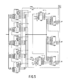
- Fig. 5 is a breadboard representation of the reset mechanism.
- the blocks U001, U002 and U003 (Signetics 74164; see Philips Data Handbook Electronic Components and Materials, Integrated Circuits Book IC09N, 1986, TTL Logic Series Signetics) form the shift register in which the preset address with the header and termination information is stored.
- the blocks U004 and U005 are recognition elements which compare the termination information and the header information with a given pattern. When correspondence is detected, the memories U007 to U011 (Signetics 74161) are loaded with the preset address.
- the blocks U006a and U006b are inverters.
- U001, U002, U003 and U007-U011 are connected to a clock signal.
- the input CLR' of U007-U011 and the input B of U001 are connected to a reset signal.
- the input CLR of U001-U003 is always high; input A is not used.
- the preset address with the header information and the termination information is input in U001-U003 via the input B and the output QH.
- Inputs ENT and ENP of U007 are high, output RCO of U007 is connected to ENT of U008 and ENP of U008-U011, RCO of U008 is connected to ENT of U009, and so on for the other memory elements.
- the 18 outputs QA, QB, QC, QD of U007-U010 and QC, QD of U011, containing the preset address, are connected to an internal memory address bus.
- Fig. 6A shows the circuit diagram of an embodiment of a reproduction apparatus comprising a picture memory device.
- Input data line 601 is connected to serial memory 605 and to synchronization signal separator 607.
- the latter is connected to control unit 609 and the reproduction element 603.
- the control unit controls the serial memory, and the user control unit 611 feeds the control unit.
- the coupling and matching means are not described for the sake of simplicity.
- Fig. 68 shows an application of preset addresses in the case of "picture in picture". Without preset addresses, the picture memory is each time completely addressed. Thanks to the improved accessibility offered by the use of preset addresses, part of the picture memory can be separately addressed without influencing the other contents. The whole operation is realized without additional connections.
Abstract
Description
- The invention relates to a serial memory, comprising a series of memory cells, data input means, data output means, control signal input means, clock signal input means and serial address input means sharing a particular terminal with said control signal input means.
- A memory of this kind is known from U.S. Patent No. 4,159,541.
- The memory described therein has only four terminals; this appears to be an absolute minimum, but such a small number reduces the flexibility; for example, all input and output data, in addition to address signals and mode-control signals, must pass through a single terminal. Furthermore, the known memory uses CCD-technology which is energy-inefficient.
- It is an object of t!' invention to provide a serial memory comprising a clock-incremented address counter and having low dissipation as well as easy accessibility.
- To achieve this, the serial memory in accordance with the invention is characterized in that the memory is suitable for the non-shifting storage of information and furthermore comprises at least one address counter suitable for accepting, under the control of an activation signal received on said control signal input means, a preset address received on said serial address input means, said at least one address counter receiving address incrementation signals from said clock signal input means.
- A first embodiment of the serial memoy is constructed so that it comprises a read address counter as well as a write address counter, each counter being selectively loadable by connection to respective associated serial address input means. This offers greater flexibility.
- In a further embodiment, the serial memory is constructed so that a reset input is used as the serial address input means. This offers the advantage of easy implementation.
- In another embodiment the serial memory is constructed so that it comprises recognition elements for header information which precedes the preset address and is receivable on the serial address input means, which header information uniquely identifies the beginning of a subsequent preset address, and/or for termination information which succeeds the preset address and which can be received on the serial address input means, which termination information uniquely identifies the end of a preceding preset address. This facilitates the detection of the preset address.
- A further embodiment of the serial memory is constructed so that said recognition elements comprise an output via which, after detection of a given pattern in said header information, a signal is supplied which ensures that the normal function of said input means, used as the serial address input means and also usable for another signal, is cancelled until the inspection of said preset address has been completed. This simplifies the input of the preset address.
- The invention also relates to a picture memory device comprising one or more of the described embodiments of serial memories, and a reproduction apparatus comprising a reproduction element and a picture memory device, of the kind set forth.
- The facility for supplying a preset address can be used in video signal processing, for example for "picture in picture" and "zoom".
- The invention will be described in detail hereinafter with reference to some Figures.
- Fig. 1 shows the interface of a known serial memory module for 256Kx4 bits,
- Fig. 2 shows a circuit diagram of the preset mechanism,
- Fig. 3 shows a timing diagram for a preferred embodiment with a header and a termination information pattern,
- Fig. 4 shows a diagram of hardware suitable for the preset mechanism,
- Fig. 5 is a breadboard representation of the reset mechanism, and
- Fig. 6 shows a reproduction apparatus comprising a picture memory device.
- Fig. 1 shows the interface of a memory module comprising separate connections for read and write operations.
- There are provided 4 inputs for data (DinO-Din3); 4 outputs for data (DoutO-Dout3); 2 connections for power supply (VDD, VSS); a write enable pin and a read enable pin (WE, RE) for (de-) activating write and read operations, respectively; a serial write clock connection and a serial read clock connection (SWCK, SRCK) for synchronization; a write reset pin and a read reset pin (RSTW, RSTR) for resetting the write address and the read address to zero, respectively, so 16 pins in total.
- In the present embodiment the reset inputs for reading and writing are used as the serial address input means for inputting the preset address with the header information and termination information.
- Fig. 2 shows the circuit diagram of the preset mechanism. Via the serial address input means (in this case one of the reset inputs) the preset address enters the associated address counter S or L which addresses, in combination with a decoder, a given memory cell MC and which subsequently counts further as from the preset address. The terms used are the same as those used in Fig. 1.
- Fig. 3A shows a timing diagram for a normal reset operation. Resetting is asynchronous in this case: in response to the transition from 0 to 1 of the reset signal RS, the address counter AC (for reading or writing) is reset to the
address 0. The address counter counts further in the rhythm of the clock signal CK (for reading or writing) The increment of the address counter is chosen to be 1 in the present case, but may also have any other arbitrary value (also a negative value) which is not equal to 0. It will be apparent also that resetting need not necessarily take place to theaddress 0, and that any other fixed address is also feasible. - Fig. 3B shows a timing diagram for a reset instruction in a preferred embodiment in which the reset input is used as the serial address input means for the input of a preset address with preceding header information and subsequent termination information. The reset signal RS is synchronised with the clock signal CK. The preset address A consists of 18 bits; the header information and the termination information consist of 3 bits each. Evidently other numbers are also possible. The address counter value becomes 0 each time when a 1 bit succeeds a 0 bit between the beginning of the header information and the end of the termination information. After the preset address with the header information and the termination information has been written into a shift register (see Fig. 4), recognition elements compare this header information and termination information with a given fixed pattern, for example 101 and 001; when correspondence is detected the preset address A between the header information and the termination information is input into the address counter: the address counter value becomes A.
- Between two successive reset instructions to a preset address the reset signal must remain stable for some clock signals (depending on the header and termination patterns chosen) in order to prevent interference.
- The normal reset function where the address counter is reset to the starting address of the memory can be maintained.
- Other versions where only header information or only termination information is used operate analogously.
- Another embodiment utilizes header information and/or termination information which ensures, after recognition by recognition elements, that a signal, is supplied which ensures that the normal reset function of the reset input is cancelled for the number of clock signals corresponding to the length of the preset address. After this time interval, the preset address is introduced into the address counter and the normal reset function of the reset input is restored.
- It will be apparent that instead of the reset input an other signal input can be used as the serial address input means, for example an enable input or a data input.
- Fig. 4 shows a diagram of hardware which is suitable for the preset mechanism: a shift register SR for writing the preset address V with the header information and termination information, II and Al, respectively, and recognition elements C1 and C2 for the header information and the termination information. When correspondence with a fixed pattern is detected, the remainder of the contents of the shift register, being the preset address V, is stored in the memory element ME of the address counter.
- Fig. 5 is a breadboard representation of the reset mechanism. The blocks U001, U002 and U003 (
Signetics 74164; see Philips Data Handbook Electronic Components and Materials, Integrated Circuits Book IC09N, 1986, TTL Logic Series Signetics) form the shift register in which the preset address with the header and termination information is stored. The blocks U004 and U005 are recognition elements which compare the termination information and the header information with a given pattern. When correspondence is detected, the memories U007 to U011 (Signetics 74161) are loaded with the preset address. The blocks U006a and U006b are inverters. - U001, U002, U003 and U007-U011 are connected to a clock signal. The input CLR' of U007-U011 and the input B of U001 are connected to a reset signal. The input CLR of U001-U003 is always high; input A is not used. In the case of a reset instruction, the preset address with the header information and the termination information is input in U001-U003 via the input B and the output QH.
- The recognition element U004 checks the correspondence (input No. 3 is'high; Nos. 2 and 4 are low) of the termination information (QC, QB and QA in U001) with pattern "001" (BO, B1, B2 = B3). Output No. 6 is connected to input No. 3 of U005. This recognition element performs the same operation on the header information. If this information alsa corresponds to the predetermined pattern (in this case "101" in B0, B1, B2 = B3), the inputs LD of U007-U011 receive a signal and the preset address (the central 18 outputs of U001-U003, numbered 0-17) is loaded via the inputs A, B, C, D of 0007-U010 and C, D of U011.
- Inputs ENT and ENP of U007 are high, output RCO of U007 is connected to ENT of U008 and ENP of U008-U011, RCO of U008 is connected to ENT of U009, and so on for the other memory elements. The 18 outputs QA, QB, QC, QD of U007-U010 and QC, QD of U011, containing the preset address, are connected to an internal memory address bus.
- Fig. 6A shows the circuit diagram of an embodiment of a reproduction apparatus comprising a picture memory device.
Input data line 601 is connected toserial memory 605 and to synchronization signal separator 607. The latter is connected to controlunit 609 and thereproduction element 603. The control unit controls the serial memory, and theuser control unit 611 feeds the control unit. The coupling and matching means are not described for the sake of simplicity. - Fig. 68 shows an application of preset addresses in the case of "picture in picture". Without preset addresses, the picture memory is each time completely addressed. Thanks to the improved accessibility offered by the use of preset addresses, part of the picture memory can be separately addressed without influencing the other contents. The whole operation is realized without additional connections.
Claims (9)
Applications Claiming Priority (2)
| Application Number | Priority Date | Filing Date | Title |
|---|---|---|---|
| NL8702672 | 1987-11-09 | ||
| NL8702672A NL8702672A (en) | 1987-11-09 | 1987-11-09 | SERIAL MEMORY, IMAGE MEMORY AND DISPLAY EQUIPPED WITH ONE OR MORE SERIAL MEMORIES. |
Publications (2)
| Publication Number | Publication Date |
|---|---|
| EP0321998A1 true EP0321998A1 (en) | 1989-06-28 |
| EP0321998B1 EP0321998B1 (en) | 1993-02-03 |
Family
ID=19850887
Family Applications (1)
| Application Number | Title | Priority Date | Filing Date |
|---|---|---|---|
| EP88202469A Expired - Lifetime EP0321998B1 (en) | 1987-11-09 | 1988-11-04 | Serial memory, picture memory device and reproduction apparatus comprising one or more serial memories |
Country Status (6)
| Country | Link |
|---|---|
| US (1) | US5046051A (en) |
| EP (1) | EP0321998B1 (en) |
| JP (1) | JP2798398B2 (en) |
| KR (1) | KR0132784B1 (en) |
| DE (1) | DE3878201T2 (en) |
| NL (1) | NL8702672A (en) |
Families Citing this family (7)
| Publication number | Priority date | Publication date | Assignee | Title |
|---|---|---|---|---|
| JPH0391188A (en) * | 1989-09-04 | 1991-04-16 | Matsushita Electric Ind Co Ltd | Fifo memory |
| EP0492025B1 (en) * | 1990-12-20 | 1997-08-06 | International Business Machines Corporation | High-speed multi-port FIFO buffer circuit |
| DE69021213T2 (en) * | 1990-12-20 | 1996-02-29 | Ibm | Modular buffer storage for a packet switched network. |
| US5206821A (en) * | 1991-07-01 | 1993-04-27 | Harris Corporation | Decimation circuit employing multiple memory data shifting section and multiple arithmetic logic unit section |
| JP4018159B2 (en) * | 1993-06-28 | 2007-12-05 | 株式会社ルネサステクノロジ | Semiconductor integrated circuit |
| JP2002281005A (en) * | 2001-03-16 | 2002-09-27 | Fujitsu Ltd | Transmission device and integrated circuit |
| CN106708277A (en) * | 2015-11-18 | 2017-05-24 | 英业达科技有限公司 | Electronic device and method for sharing input apparatus |
Citations (2)
| Publication number | Priority date | Publication date | Assignee | Title |
|---|---|---|---|---|
| US4159541A (en) * | 1977-07-01 | 1979-06-26 | Ncr Corporation | Minimum pin memory device |
| WO1979000912A1 (en) * | 1978-04-11 | 1979-11-15 | Ncr Co | Memory device having a minimum number of pins |
Family Cites Families (6)
| Publication number | Priority date | Publication date | Assignee | Title |
|---|---|---|---|---|
| JPS5215257U (en) * | 1975-07-21 | 1977-02-03 | ||
| SE424510B (en) * | 1975-08-26 | 1982-07-26 | Inventing Ab | SET AND DEVICE FOR DOUBLE SIDE COATING OF A CURRENT COAT |
| JPS6228993A (en) * | 1985-07-30 | 1987-02-06 | Toshiba Corp | Memory device |
| US4751675A (en) * | 1985-08-19 | 1988-06-14 | American Telephone And Telegraph Company, At&T Bell Laboratories | Memory access circuit with pointer shifting network |
| JPS62209792A (en) * | 1986-03-11 | 1987-09-14 | Fujitsu Ltd | Fifo circuit |
| US4813015A (en) * | 1986-03-12 | 1989-03-14 | Advanced Micro Devices, Inc. | Fracturable x-y storage array using a ram cell with bidirectional shift |
-
1987
- 1987-11-09 NL NL8702672A patent/NL8702672A/en not_active Application Discontinuation
-
1988
- 1988-11-04 EP EP88202469A patent/EP0321998B1/en not_active Expired - Lifetime
- 1988-11-04 DE DE8888202469T patent/DE3878201T2/en not_active Expired - Fee Related
- 1988-11-08 KR KR1019880014643A patent/KR0132784B1/en not_active IP Right Cessation
- 1988-11-08 JP JP63280534A patent/JP2798398B2/en not_active Expired - Fee Related
- 1988-11-09 US US07/269,229 patent/US5046051A/en not_active Expired - Lifetime
Patent Citations (2)
| Publication number | Priority date | Publication date | Assignee | Title |
|---|---|---|---|---|
| US4159541A (en) * | 1977-07-01 | 1979-06-26 | Ncr Corporation | Minimum pin memory device |
| WO1979000912A1 (en) * | 1978-04-11 | 1979-11-15 | Ncr Co | Memory device having a minimum number of pins |
Non-Patent Citations (3)
| Title |
|---|
| IEEE JOURNAL OF SOLID-STATE CIRCUITS, vol. SC-16, no. 3, June 1981, pages 190-194, IEEE, New York, US; G. MEUSBURGER: "1.5 V 1 K-CMOS-RAM with only 8 pins" * |
| PATENT ABSTRACTS OF JAPAN, vol. 5, no. 36 (P-51)[708], 7th March 1981; & JP-A-55 157 177 (TOKYO SHIBAURA DENKI K.K.) 06-12-1980 * |
| PATENT ABSTRACTS OF JAPAN, vol. 7, no. 206 (P-222)[1351], 10th September 1983; & JP-A-58 101 320 (FUJITSUU DENSOU K.K.) 16-06-1983 * |
Also Published As
| Publication number | Publication date |
|---|---|
| NL8702672A (en) | 1989-06-01 |
| DE3878201D1 (en) | 1993-03-18 |
| KR0132784B1 (en) | 1998-10-01 |
| JPH01155596A (en) | 1989-06-19 |
| US5046051A (en) | 1991-09-03 |
| DE3878201T2 (en) | 1993-07-22 |
| KR890008823A (en) | 1989-07-12 |
| JP2798398B2 (en) | 1998-09-17 |
| EP0321998B1 (en) | 1993-02-03 |
Similar Documents
| Publication | Publication Date | Title |
|---|---|---|
| US5727207A (en) | Method and apparatus for automatically loading configuration data on reset into a host adapter integrated circuit | |
| US6002638A (en) | Memory device having a switchable clock output and method therefor | |
| US5386539A (en) | IC memory card comprising an EEPROM with data and address buffering for controlling the writing/reading of data to EEPROM | |
| US4159541A (en) | Minimum pin memory device | |
| EP0249548A2 (en) | Dual-port semiconductor memory device | |
| US5663922A (en) | Method for the anticipated reading of serial access memory, and memory pertaining thereto | |
| KR890008829A (en) | Semiconductor memory | |
| GB2232797A (en) | Ram based serial memory with pipelined look-ahead reading | |
| KR0174266B1 (en) | Single semiconductor substrate ram device utilizing data compressing/expanding mechanism in a multi-microprocessor e.. | |
| EP0321998B1 (en) | Serial memory, picture memory device and reproduction apparatus comprising one or more serial memories | |
| EP0362050B1 (en) | Memory card | |
| US5781796A (en) | System for automatic configuration of I/O base address without configuration program using readout data on common bus by responding device | |
| US5307472A (en) | Data transfer interface module | |
| US5500810A (en) | Filter device with memory test circuit | |
| KR930004178B1 (en) | Testing circuit in semiconductor memory device | |
| KR0179166B1 (en) | Memory device for digital image signal processing | |
| US5548778A (en) | System for assigning device to be connected to computer when address from computer is effective by comparing address for entire memory space and found coincided | |
| US6088271A (en) | Method and apparatus for transferring signal to circuit without waveform distortion | |
| KR200148658Y1 (en) | A circuit selecting input/output card of plc | |
| KR100214461B1 (en) | Memory card of searching password | |
| JP2683348B2 (en) | Card memory | |
| JPH01236389A (en) | Memory card | |
| SU1098002A1 (en) | Memory access control unit | |
| JPH06188871A (en) | Frame aligner circuit | |
| JPS6337885A (en) | Memory card |
Legal Events
| Date | Code | Title | Description |
|---|---|---|---|
| PUAI | Public reference made under article 153(3) epc to a published international application that has entered the european phase |
Free format text: ORIGINAL CODE: 0009012 |
|
| AK | Designated contracting states |
Kind code of ref document: A1 Designated state(s): DE ES FR GB IT |
|
| 17P | Request for examination filed |
Effective date: 19891218 |
|
| 17Q | First examination report despatched |
Effective date: 19920325 |
|
| GRAA | (expected) grant |
Free format text: ORIGINAL CODE: 0009210 |
|
| AK | Designated contracting states |
Kind code of ref document: B1 Designated state(s): DE ES FR GB IT |
|
| PG25 | Lapsed in a contracting state [announced via postgrant information from national office to epo] |
Ref country code: ES Free format text: THE PATENT HAS BEEN ANNULLED BY A DECISION OF A NATIONAL AUTHORITY Effective date: 19930203 |
|
| ITF | It: translation for a ep patent filed |
Owner name: ING. C. GREGORJ S.P.A. |
|
| REF | Corresponds to: |
Ref document number: 3878201 Country of ref document: DE Date of ref document: 19930318 |
|
| ET | Fr: translation filed | ||
| PLBE | No opposition filed within time limit |
Free format text: ORIGINAL CODE: 0009261 |
|
| STAA | Information on the status of an ep patent application or granted ep patent |
Free format text: STATUS: NO OPPOSITION FILED WITHIN TIME LIMIT |
|
| 26N | No opposition filed | ||
| ITPR | It: changes in ownership of a european patent |
Owner name: CAMBIO RAGIONE SOCIALE;PHILIPS ELECTRONICS N.V. |
|
| REG | Reference to a national code |
Ref country code: FR Ref legal event code: CD |
|
| REG | Reference to a national code |
Ref country code: FR Ref legal event code: CD |
|
| REG | Reference to a national code |
Ref country code: GB Ref legal event code: IF02 |
|
| PGFP | Annual fee paid to national office [announced via postgrant information from national office to epo] |
Ref country code: GB Payment date: 20061127 Year of fee payment: 19 |
|
| PGFP | Annual fee paid to national office [announced via postgrant information from national office to epo] |
Ref country code: FR Payment date: 20061129 Year of fee payment: 19 |
|
| PGFP | Annual fee paid to national office [announced via postgrant information from national office to epo] |
Ref country code: IT Payment date: 20061130 Year of fee payment: 19 |
|
| PGFP | Annual fee paid to national office [announced via postgrant information from national office to epo] |
Ref country code: DE Payment date: 20070110 Year of fee payment: 19 |
|
| GBPC | Gb: european patent ceased through non-payment of renewal fee |
Effective date: 20071104 |
|
| PG25 | Lapsed in a contracting state [announced via postgrant information from national office to epo] |
Ref country code: DE Free format text: LAPSE BECAUSE OF NON-PAYMENT OF DUE FEES Effective date: 20080603 |
|
| REG | Reference to a national code |
Ref country code: FR Ref legal event code: ST Effective date: 20080930 |
|
| PG25 | Lapsed in a contracting state [announced via postgrant information from national office to epo] |
Ref country code: GB Free format text: LAPSE BECAUSE OF NON-PAYMENT OF DUE FEES Effective date: 20071104 |
|
| PG25 | Lapsed in a contracting state [announced via postgrant information from national office to epo] |
Ref country code: FR Free format text: LAPSE BECAUSE OF NON-PAYMENT OF DUE FEES Effective date: 20071130 |
|
| PG25 | Lapsed in a contracting state [announced via postgrant information from national office to epo] |
Ref country code: IT Free format text: LAPSE BECAUSE OF NON-PAYMENT OF DUE FEES Effective date: 20071104 |