EP0321239A2 - Fabricating method of semiconductor device - Google Patents
Fabricating method of semiconductor device Download PDFInfo
- Publication number
- EP0321239A2 EP0321239A2 EP88311869A EP88311869A EP0321239A2 EP 0321239 A2 EP0321239 A2 EP 0321239A2 EP 88311869 A EP88311869 A EP 88311869A EP 88311869 A EP88311869 A EP 88311869A EP 0321239 A2 EP0321239 A2 EP 0321239A2
- Authority
- EP
- European Patent Office
- Prior art keywords
- semiconductor device
- electrode
- wiring
- conductor
- conductor wiring
- Prior art date
- Legal status (The legal status is an assumption and is not a legal conclusion. Google has not performed a legal analysis and makes no representation as to the accuracy of the status listed.)
- Withdrawn
Links
Images

Classifications
-
- H—ELECTRICITY
- H01—ELECTRIC ELEMENTS
- H01L—SEMICONDUCTOR DEVICES NOT COVERED BY CLASS H10
- H01L21/00—Processes or apparatus adapted for the manufacture or treatment of semiconductor or solid state devices or of parts thereof
- H01L21/02—Manufacture or treatment of semiconductor devices or of parts thereof
- H01L21/04—Manufacture or treatment of semiconductor devices or of parts thereof the devices having at least one potential-jump barrier or surface barrier, e.g. PN junction, depletion layer or carrier concentration layer
- H01L21/50—Assembly of semiconductor devices using processes or apparatus not provided for in a single one of the subgroups H01L21/06 - H01L21/326, e.g. sealing of a cap to a base of a container
- H01L21/56—Encapsulations, e.g. encapsulation layers, coatings
- H01L21/563—Encapsulation of active face of flip-chip device, e.g. underfilling or underencapsulation of flip-chip, encapsulation preform on chip or mounting substrate
-
- H—ELECTRICITY
- H01—ELECTRIC ELEMENTS
- H01L—SEMICONDUCTOR DEVICES NOT COVERED BY CLASS H10
- H01L21/00—Processes or apparatus adapted for the manufacture or treatment of semiconductor or solid state devices or of parts thereof
- H01L21/02—Manufacture or treatment of semiconductor devices or of parts thereof
- H01L21/04—Manufacture or treatment of semiconductor devices or of parts thereof the devices having at least one potential-jump barrier or surface barrier, e.g. PN junction, depletion layer or carrier concentration layer
- H01L21/50—Assembly of semiconductor devices using processes or apparatus not provided for in a single one of the subgroups H01L21/06 - H01L21/326, e.g. sealing of a cap to a base of a container
- H01L21/60—Attaching or detaching leads or other conductive members, to be used for carrying current to or from the device in operation
-
- H—ELECTRICITY
- H01—ELECTRIC ELEMENTS
- H01L—SEMICONDUCTOR DEVICES NOT COVERED BY CLASS H10
- H01L24/00—Arrangements for connecting or disconnecting semiconductor or solid-state bodies; Methods or apparatus related thereto
- H01L24/01—Means for bonding being attached to, or being formed on, the surface to be connected, e.g. chip-to-package, die-attach, "first-level" interconnects; Manufacturing methods related thereto
- H01L24/26—Layer connectors, e.g. plate connectors, solder or adhesive layers; Manufacturing methods related thereto
- H01L24/28—Structure, shape, material or disposition of the layer connectors prior to the connecting process
- H01L24/29—Structure, shape, material or disposition of the layer connectors prior to the connecting process of an individual layer connector
-
- H—ELECTRICITY
- H01—ELECTRIC ELEMENTS
- H01L—SEMICONDUCTOR DEVICES NOT COVERED BY CLASS H10
- H01L2224/00—Indexing scheme for arrangements for connecting or disconnecting semiconductor or solid-state bodies and methods related thereto as covered by H01L24/00
- H01L2224/01—Means for bonding being attached to, or being formed on, the surface to be connected, e.g. chip-to-package, die-attach, "first-level" interconnects; Manufacturing methods related thereto
- H01L2224/10—Bump connectors; Manufacturing methods related thereto
- H01L2224/15—Structure, shape, material or disposition of the bump connectors after the connecting process
- H01L2224/16—Structure, shape, material or disposition of the bump connectors after the connecting process of an individual bump connector
- H01L2224/161—Disposition
- H01L2224/16151—Disposition the bump connector connecting between a semiconductor or solid-state body and an item not being a semiconductor or solid-state body, e.g. chip-to-substrate, chip-to-passive
- H01L2224/16221—Disposition the bump connector connecting between a semiconductor or solid-state body and an item not being a semiconductor or solid-state body, e.g. chip-to-substrate, chip-to-passive the body and the item being stacked
- H01L2224/16225—Disposition the bump connector connecting between a semiconductor or solid-state body and an item not being a semiconductor or solid-state body, e.g. chip-to-substrate, chip-to-passive the body and the item being stacked the item being non-metallic, e.g. insulating substrate with or without metallisation
-
- H—ELECTRICITY
- H01—ELECTRIC ELEMENTS
- H01L—SEMICONDUCTOR DEVICES NOT COVERED BY CLASS H10
- H01L2224/00—Indexing scheme for arrangements for connecting or disconnecting semiconductor or solid-state bodies and methods related thereto as covered by H01L24/00
- H01L2224/73—Means for bonding being of different types provided for in two or more of groups H01L2224/10, H01L2224/18, H01L2224/26, H01L2224/34, H01L2224/42, H01L2224/50, H01L2224/63, H01L2224/71
- H01L2224/732—Location after the connecting process
- H01L2224/73201—Location after the connecting process on the same surface
- H01L2224/73203—Bump and layer connectors
- H01L2224/73204—Bump and layer connectors the bump connector being embedded into the layer connector
-
- H—ELECTRICITY
- H01—ELECTRIC ELEMENTS
- H01L—SEMICONDUCTOR DEVICES NOT COVERED BY CLASS H10
- H01L2224/00—Indexing scheme for arrangements for connecting or disconnecting semiconductor or solid-state bodies and methods related thereto as covered by H01L24/00
- H01L2224/80—Methods for connecting semiconductor or other solid state bodies using means for bonding being attached to, or being formed on, the surface to be connected
- H01L2224/83—Methods for connecting semiconductor or other solid state bodies using means for bonding being attached to, or being formed on, the surface to be connected using a layer connector
- H01L2224/8319—Arrangement of the layer connectors prior to mounting
- H01L2224/83192—Arrangement of the layer connectors prior to mounting wherein the layer connectors are disposed only on another item or body to be connected to the semiconductor or solid-state body
-
- H—ELECTRICITY
- H01—ELECTRIC ELEMENTS
- H01L—SEMICONDUCTOR DEVICES NOT COVERED BY CLASS H10
- H01L2924/00—Indexing scheme for arrangements or methods for connecting or disconnecting semiconductor or solid-state bodies as covered by H01L24/00
- H01L2924/01—Chemical elements
- H01L2924/01006—Carbon [C]
-
- H—ELECTRICITY
- H01—ELECTRIC ELEMENTS
- H01L—SEMICONDUCTOR DEVICES NOT COVERED BY CLASS H10
- H01L2924/00—Indexing scheme for arrangements or methods for connecting or disconnecting semiconductor or solid-state bodies as covered by H01L24/00
- H01L2924/01—Chemical elements
- H01L2924/01013—Aluminum [Al]
-
- H—ELECTRICITY
- H01—ELECTRIC ELEMENTS
- H01L—SEMICONDUCTOR DEVICES NOT COVERED BY CLASS H10
- H01L2924/00—Indexing scheme for arrangements or methods for connecting or disconnecting semiconductor or solid-state bodies as covered by H01L24/00
- H01L2924/01—Chemical elements
- H01L2924/01015—Phosphorus [P]
-
- H—ELECTRICITY
- H01—ELECTRIC ELEMENTS
- H01L—SEMICONDUCTOR DEVICES NOT COVERED BY CLASS H10
- H01L2924/00—Indexing scheme for arrangements or methods for connecting or disconnecting semiconductor or solid-state bodies as covered by H01L24/00
- H01L2924/01—Chemical elements
- H01L2924/01024—Chromium [Cr]
-
- H—ELECTRICITY
- H01—ELECTRIC ELEMENTS
- H01L—SEMICONDUCTOR DEVICES NOT COVERED BY CLASS H10
- H01L2924/00—Indexing scheme for arrangements or methods for connecting or disconnecting semiconductor or solid-state bodies as covered by H01L24/00
- H01L2924/01—Chemical elements
- H01L2924/01029—Copper [Cu]
-
- H—ELECTRICITY
- H01—ELECTRIC ELEMENTS
- H01L—SEMICONDUCTOR DEVICES NOT COVERED BY CLASS H10
- H01L2924/00—Indexing scheme for arrangements or methods for connecting or disconnecting semiconductor or solid-state bodies as covered by H01L24/00
- H01L2924/01—Chemical elements
- H01L2924/01033—Arsenic [As]
-
- H—ELECTRICITY
- H01—ELECTRIC ELEMENTS
- H01L—SEMICONDUCTOR DEVICES NOT COVERED BY CLASS H10
- H01L2924/00—Indexing scheme for arrangements or methods for connecting or disconnecting semiconductor or solid-state bodies as covered by H01L24/00
- H01L2924/01—Chemical elements
- H01L2924/01046—Palladium [Pd]
-
- H—ELECTRICITY
- H01—ELECTRIC ELEMENTS
- H01L—SEMICONDUCTOR DEVICES NOT COVERED BY CLASS H10
- H01L2924/00—Indexing scheme for arrangements or methods for connecting or disconnecting semiconductor or solid-state bodies as covered by H01L24/00
- H01L2924/01—Chemical elements
- H01L2924/01047—Silver [Ag]
-
- H—ELECTRICITY
- H01—ELECTRIC ELEMENTS
- H01L—SEMICONDUCTOR DEVICES NOT COVERED BY CLASS H10
- H01L2924/00—Indexing scheme for arrangements or methods for connecting or disconnecting semiconductor or solid-state bodies as covered by H01L24/00
- H01L2924/01—Chemical elements
- H01L2924/0105—Tin [Sn]
-
- H—ELECTRICITY
- H01—ELECTRIC ELEMENTS
- H01L—SEMICONDUCTOR DEVICES NOT COVERED BY CLASS H10
- H01L2924/00—Indexing scheme for arrangements or methods for connecting or disconnecting semiconductor or solid-state bodies as covered by H01L24/00
- H01L2924/01—Chemical elements
- H01L2924/01078—Platinum [Pt]
-
- H—ELECTRICITY
- H01—ELECTRIC ELEMENTS
- H01L—SEMICONDUCTOR DEVICES NOT COVERED BY CLASS H10
- H01L2924/00—Indexing scheme for arrangements or methods for connecting or disconnecting semiconductor or solid-state bodies as covered by H01L24/00
- H01L2924/01—Chemical elements
- H01L2924/01079—Gold [Au]
-
- H—ELECTRICITY
- H01—ELECTRIC ELEMENTS
- H01L—SEMICONDUCTOR DEVICES NOT COVERED BY CLASS H10
- H01L2924/00—Indexing scheme for arrangements or methods for connecting or disconnecting semiconductor or solid-state bodies as covered by H01L24/00
- H01L2924/095—Indexing scheme for arrangements or methods for connecting or disconnecting semiconductor or solid-state bodies as covered by H01L24/00 with a principal constituent of the material being a combination of two or more materials provided in the groups H01L2924/013 - H01L2924/0715
- H01L2924/097—Glass-ceramics, e.g. devitrified glass
- H01L2924/09701—Low temperature co-fired ceramic [LTCC]
-
- H—ELECTRICITY
- H01—ELECTRIC ELEMENTS
- H01L—SEMICONDUCTOR DEVICES NOT COVERED BY CLASS H10
- H01L2924/00—Indexing scheme for arrangements or methods for connecting or disconnecting semiconductor or solid-state bodies as covered by H01L24/00
- H01L2924/10—Details of semiconductor or other solid state devices to be connected
- H01L2924/11—Device type
- H01L2924/14—Integrated circuits
Definitions
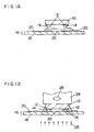
- This invention relates to a fabricating method of semiconductor device, and more particularly to a mounting method of LSI chips of multiple electrodes and narrow pitch in microcomputer, gate array, etc.
- a semiconductor device e.g., an IC chip
- a multi-layer metal film is formed and fixed on each electrode pad 12 of semiconductor device 10.
- the multi-layer metal film is made by Cr-Cu, Ti-Pd, etc.
- Metal projection or metal bump 14 is formed on each electrode pad 12 by conventional electro-plating method.
- the metal bump 14 is made by Au, Ag, Cu solder, etc. and its thickness is 3-30 ⁇ m.
- the wiring board 16 includes base 18 and wiring pattern 20 which is formed on the base 18.
- the base 18 is made by glass, ceramic, resin or, metal whose surface is covered by metal oxide, and so on.
- the wiring patterns 20 are formed on a surface of base 18 and designed to receive corresponding metal bumps 14 of semiconductor device 10.
- the wiring patterns 20 include, as principal material, Cu, Al, Au, ITO, etc., and for example, when Cu (which is readily oxidized) is selected as principal material, Au plating, Sn plating, solder plating, etc. is applied thereto.
- insulating synthetic resin 22 is disposed on wiring board 16 at the position to which semiconductor device 10 is attached.
- the resin 22 may be disposed on a bottom surface of semiconductor device 10.
- the resin 22 may be liquid or sheet material, and solidified by light or heat.
- the resin 22 may be a modified acrylate.
- the semiconductor device 10 is held by a movable tool 24 and positions o metal bumps 14 are adjusted to be in correspondence with wiring patterns 20 of wiring board 16. Then, metal bumps 14 are pressed against wiring pattern 20 by downward movement of tool 24 in the direction of arrow 26. By this pressure applied in the direction of arrow 26, resin 22, which is disposed between metal bump 14 and wiring pattern 20, is pressed to be expanded outwardly so that resin 22 is removed from the area between metal bump 14 and wiring pattern 20 and metal bumps 14 are electrically connected to wiring pattern 20.
- the electrical connection of metal bumps 14 of semiconductor device 10 and wiring pattern 20 of wiring board 16 is accomplished by the application of pressure, and the fixing of semiconductor device 10 and wiring board 16 is accomplished by stiffened resin.
- the resin 22 is of a modified acrylate group.
- the stiffening operation is completed by the application of ultraviolet light of 300-400 nm for approximately 20-60 seconds at an energy of 20 mW/cm2.
- the stiffening operation is completed by application of heat whose temperature is 100°-150° for 5-30 minutes.
- electrical resistance of the connection portion becomes approximately 1-10 mohms.
- insulating resin 22 is of a combination type, e.g., light stiffening and natural stiffening
- light application may be carried out both from the semiconductor device side (upper side in FIG. 1) and from the wiring board side (lower side) because, even if an unstiffened portion of resin 22 remains; it is stiffened by the lapse of time.
- insulating resin 22 is of another combination type, e.g. light stiffening and heat stiffening, a part of the resin is stiffened by light application so that semiconductor device 10 and wiring board 16 are temporarily fixed, and thereafter, they are completely fixed by heat application.
- the fabricating method of semiconductor device of this invention is to keep the bump electrode of LSI chip in elastic deformation when pressing the LSI chip to a wiring board, and to connect the bump electrode of the LSI chip and the conductor wiring.
- This invention possesses the following advantages. Since the bump electrode of the LSI chip is set in contact with the conductor wiring of the wiring board in an elastic deformation state, if a dimensional change due to thermal expansion occurs in the insulating resin, or if a dimensional change between the LSI chip and wiring board occurs, the bump electrodes recovers elastically, so that the contact state of the bump electrode and conductor wiring may be always maintained, and the heat resistance and reliability may be high. It is hence possible to apply into power device or the like.
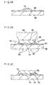
- a light- or heat-stiffening insulating resin 34 is applied in a region containing a conductor wiring 30 of wiring board 32 possessing a conductor wiring 30 made of glass or ceramic.
- the thickness of the wiring board 32 is about 0.1 to 2.0 mm
- the conductor wiring 30 is CR-Au, Al, ITO, etc., and its thickness is about 0.1 to 10 ⁇ m.
- the insulating resin 34 is an acrylic, epoxy or similar material which is stiffened by ultraviolet rays or both ultraviolet rays and heat, and it is applied by dispenser, screen printing or other means.
- an LSI chip 38 having a bump electrode 36 made of Au or the like is disposed in a region coated with the insualting resin 34 of the wiring board 32 so that the bump electrode 36 and the conductor wiring 30 may coincide with each other.
- the thickness of the bump electrode 36 is about 5 to 30 ⁇ m, and its dimension is about 3 to 50 ⁇ m square.
- the LSI chip 38 is pressed by a pressing tool 40.
- the pressure is about 0.5 g/electrode to 5 g/electrode.
- FIGS. 3A, 3B The state of elastic deformation of the bump electrode 36 is shown in FIGS. 3A, 3B.
- FIG. 3A shows the LSI chip 38 being placed at the position of the wiring board 32
- FIG. 3B denotes the state of pressing the LSI chip 38 and elastically deforming the bump electrode 36. Since the bump electrode 36 is in an elastic deformation state, if the insulating resin 34 is later stiffened and relieved, a restoring force acts on the bump electrode 36, and the contact pressure of the bump electrode f36 on the conductor wiring 30 is strong, and it also follows up the dimensional change due to expansion of the insulating resin 36 after stiffening, the contact resistance remains high even at high temperature, and a high reliability is obtained.
- the insulating resin 34 is forced outward, and the bump electrode 36 of the LSI chip 38 and the conductor wiring 30 electrically contact with each other.
- the insulating resin 34 is heated, and is irradiated with ultraviolet rays 42, 44 at the same time to stiffen the insulating resin 34.
- the wiring board 32 is a glass, it is irradiated with ultraviolet rays 42, or if it is an opaque board such as ceramic, the side face of the LSI chip 38 is irradiated with ultraviolet ray 44.
- a heating mechanism is installed, for example, in the pressing tool 40. Or it may be also possible to heat easily by using infrared rays or hot air.
- the heating time is about 0.5 to 1.0 second. Afterwards, the heating tool 40 is canceled. At this time, the LSI chip is affixed to the wiring board 32 by means of the insulating resin 34, and the bump electrode 36 of the LSI chip and conductor wiring 30 are electrically connected with each other by contact.
Abstract
Description
- This invention relates to a fabricating method of semiconductor device, and more particularly to a mounting method of LSI chips of multiple electrodes and narrow pitch in microcomputer, gate array, etc.
- The present inventors already proposed the following method as a method suited to mounting of such devices (Japanese Ladi-Open Patent No. 60-262430, corresponding to U.S. Application No. 943,197, now issued as U.S.P. 4,749,120).
- An example of the previously proposed art is described with reference to FIG. 1. A semiconductor device (e.g., an IC chip) is designated by
numeral 10. A multi-layer metal film is formed and fixed on eachelectrode pad 12 ofsemiconductor device 10. The multi-layer metal film is made by Cr-Cu, Ti-Pd, etc. Metal projection ormetal bump 14 is formed on eachelectrode pad 12 by conventional electro-plating method. Themetal bump 14 is made by Au, Ag, Cu solder, etc. and its thickness is 3-30 µm. - On the other hand, a wiring board is designated by numeral 16. The wiring board 16 includes
base 18 andwiring pattern 20 which is formed on thebase 18. Thebase 18 is made by glass, ceramic, resin or, metal whose surface is covered by metal oxide, and so on. Thewiring patterns 20 are formed on a surface ofbase 18 and designed to receivecorresponding metal bumps 14 ofsemiconductor device 10. Thewiring patterns 20 include, as principal material, Cu, Aℓ, Au, ITO, etc., and for example, when Cu (which is readily oxidized) is selected as principal material, Au plating, Sn plating, solder plating, etc. is applied thereto. - Further, insulating
synthetic resin 22 is disposed on wiring board 16 at the position to whichsemiconductor device 10 is attached. Theresin 22 may be disposed on a bottom surface ofsemiconductor device 10. Theresin 22 may be liquid or sheet material, and solidified by light or heat. Theresin 22 may be a modified acrylate. - The
semiconductor device 10 is held by amovable tool 24 and positions ometal bumps 14 are adjusted to be in correspondence withwiring patterns 20 of wiring board 16. Then,metal bumps 14 are pressed againstwiring pattern 20 by downward movement oftool 24 in the direction of arrow 26. By this pressure applied in the direction of arrow 26,resin 22, which is disposed betweenmetal bump 14 andwiring pattern 20, is pressed to be expanded outwardly so thatresin 22 is removed from the area betweenmetal bump 14 andwiring pattern 20 andmetal bumps 14 are electrically connected towiring pattern 20. - In this position, light or
heat 28 is applied to resin 22. Thereby,resin 22 is stiffened or solidified. By suchstiffened resin 22,semiconductor device 10 and wiring baord 16 are fixed withmetal bumps 14 being electrically connected towiring patterns 20. Thereafter, light or heat (28) application is stopped and then, pressure (26) application is removed. - As explained above, in the first embodiment, the electrical connection of
metal bumps 14 ofsemiconductor device 10 andwiring pattern 20 of wiring board 16 is accomplished by the application of pressure, and the fixing ofsemiconductor device 10 and wiring board 16 is accomplished by stiffened resin. - The
resin 22 is of a modified acrylate group. In the case thatresin 22 is stiffened by light, the stiffening operation is completed by the application of ultraviolet light of 300-400 nm for approximately 20-60 seconds at an energy of 20 mW/cm². In the case of stiffening by use of heat, the stiffening operation is completed by application of heat whose temperature is 100°-150° for 5-30 minutes. In these cases, given a surface zie ofmetal pump 14 is 70x70 µm andmetal bump 14 being made of Au, electrical resistance of the connection portion becomes approximately 1-10 mohms. - If
insulating resin 22 is of a combination type, e.g., light stiffening and natural stiffening, light application may be carried out both from the semiconductor device side (upper side in FIG. 1) and from the wiring board side (lower side) because, even if an unstiffened portion ofresin 22 remains; it is stiffened by the lapse of time. - If insulating
resin 22 is of another combination type, e.g. light stiffening and heat stiffening, a part of the resin is stiffened by light application so thatsemiconductor device 10 and wiring board 16 are temporarily fixed, and thereafter, they are completely fixed by heat application. - If these cases, fixing can be accomplished with a higher reliability by the use of pressure application when unstiffened resin is stiffened at normal temperature or by heating after light application is completed. In this case, there arises no problem even if the pressure to be applied is less than that upon light application.
- It is hence a primary object of this invention to further enhance the reliability and productivity of the above proposal.
- To achieve this object, the fabricating method of semiconductor device of this invention is to keep the bump electrode of LSI chip in elastic deformation when pressing the LSI chip to a wiring board, and to connect the bump electrode of the LSI chip and the conductor wiring.
- This invention possesses the following advantages. Since the bump electrode of the LSI chip is set in contact with the conductor wiring of the wiring board in an elastic deformation state, if a dimensional change due to thermal expansion occurs in the insulating resin, or if a dimensional change between the LSI chip and wiring board occurs, the bump electrodes recovers elastically, so that the contact state of the bump electrode and conductor wiring may be always maintained, and the heat resistance and reliability may be high. It is hence possible to apply into power device or the like.
- FIG. 1 shows an example of the previously proposed art;
- FIG. 2 shows an embodiment of this invention; and
- FIG.3 shows a state of elastic deformation of the bump electrode in this invention.
- An embodiment of the invention is described below while referring to FIG. 2.
- First, as shown in FIG. 2A, a light- or heat-stiffening
insulating resin 34 is applied in a region containing aconductor wiring 30 ofwiring board 32 possessing aconductor wiring 30 made of glass or ceramic. The thickness of thewiring board 32 is about 0.1 to 2.0 mm, and theconductor wiring 30 is CR-Au, Aℓ, ITO, etc., and its thickness is about 0.1 to 10 µm. Theinsulating resin 34 is an acrylic, epoxy or similar material which is stiffened by ultraviolet rays or both ultraviolet rays and heat, and it is applied by dispenser, screen printing or other means. Next, as shwon in FIG. 2B, anLSI chip 38 having abump electrode 36 made of Au or the like is disposed in a region coated with theinsualting resin 34 of thewiring board 32 so that thebump electrode 36 and theconductor wiring 30 may coincide with each other. - The thickness of the
bump electrode 36 is about 5 to 30 µm, and its dimension is about 3 to 50 µm square. In order to keep thebump electrode 36 in an elastic deformation state, theLSI chip 38 is pressed by apressing tool 40. The pressure is about 0.5 g/electrode to 5 g/electrode. - The state of elastic deformation of the
bump electrode 36 is shown in FIGS. 3A, 3B. FIG. 3A shows theLSI chip 38 being placed at the position of thewiring board 32, and FIG. 3B denotes the state of pressing theLSI chip 38 and elastically deforming thebump electrode 36. Since thebump electrode 36 is in an elastic deformation state, if theinsulating resin 34 is later stiffened and relieved, a restoring force acts on thebump electrode 36, and the contact pressure of the bump electrode f36 on theconductor wiring 30 is strong, and it also follows up the dimensional change due to expansion of theinsulating resin 36 after stiffening, the contact resistance remains high even at high temperature, and a high reliability is obtained. - At this time, the
insulating resin 34 is forced outward, and thebump electrode 36 of theLSI chip 38 and the conductor wiring 30 electrically contact with each other. - Next, with the
LSI chip 38 being pressed, theinsulating resin 34 is heated, and is irradiated withultraviolet rays insulating resin 34. If thewiring board 32 is a glass, it is irradiated withultraviolet rays 42, or if it is an opaque board such as ceramic, the side face of theLSI chip 38 is irradiated withultraviolet ray 44. To heat theinsulating resin 34, a heating mechanism is installed, for example, in thepressing tool 40. Or it may be also possible to heat easily by using infrared rays or hot air. In this way, by irradiating with ultraviolet rays while heating theinsulating resin 34, it is possible to stiffen in a very short time. For example, at the heating temperature of 100°C and ultraviolet ray illumination fo 500 to 1000 mW/cm², the heating time is about 0.5 to 1.0 second. Afterwards, theheating tool 40 is canceled. At this time, the LSI chip is affixed to thewiring board 32 by means of the insulatingresin 34, and thebump electrode 36 of the LSI chip andconductor wiring 30 are electrically connected with each other by contact.
Claims (4)
a step of applying an insulating resin to a conductor wiring part of an insulation substrate having the conductor wiring;
a step of matching the conductor wiring and the electrode of the semiconductor device, pressing the semiconductor device to the applied region of the insulating resin of the insualtion substrate, and connecting the conductor wiring in the state of elastic deformation of the semiconductor device, and
a step of stiffening the insulating resin and affixing the semiconductor device to the insulation substrate, while electrically connecting the conductor wiring and the electrode of the semiconductor device.
a step of applying an insulating resin to a conductor wiring part of an insulation substrate having the conductor wiring;
a step of matching the conductor wiring with the electrode of the semiconductor device, pressing the semiconductor device to the applied region of the insulating resin of the insulation substrate, and contacting the electrode of the semiconductor device with the conductor wiring; and
a step of stiffening the insulating resin by irradiating with ultraviolet rays and heating at the same time to affix the semiconductor device to the insulation substrate, and electrically connecting the conductor wiring and the electrode of the semiconductor device.
a step of applying an insulating resin to a conductor wiring part of an insulation substrate having the conductor wiring;
a step of matching the conductor wiring with the electrode of the semiconductor device, pressing the semiconductor device to the applied region of the insulating resin of the insulation substrate, and contacting the conductor wiring with the electrode of the semiconductor device kept in an elastically deformed state; and
a step of stiffening the insulation resin by irradiating with ultraviolet rays and heating at the same time to affix the semiconductor device to the insulation substrate, while electrically connecting the conductor wiring and the electrode of the semiconductor device.
Applications Claiming Priority (2)
| Application Number | Priority Date | Filing Date | Title |
|---|---|---|---|
| JP319444/87 | 1987-12-17 | ||
| JP62319444A JPH01160029A (en) | 1987-12-17 | 1987-12-17 | Semiconductor device |
Publications (2)
| Publication Number | Publication Date |
|---|---|
| EP0321239A2 true EP0321239A2 (en) | 1989-06-21 |
| EP0321239A3 EP0321239A3 (en) | 1990-04-25 |
Family
ID=18110268
Family Applications (1)
| Application Number | Title | Priority Date | Filing Date |
|---|---|---|---|
| EP88311869A Withdrawn EP0321239A3 (en) | 1987-12-17 | 1988-12-15 | Fabricating method of semiconductor device |
Country Status (3)
| Country | Link |
|---|---|
| EP (1) | EP0321239A3 (en) |
| JP (1) | JPH01160029A (en) |
| KR (1) | KR920002075B1 (en) |
Cited By (5)
| Publication number | Priority date | Publication date | Assignee | Title |
|---|---|---|---|---|
| EP0449496A1 (en) * | 1990-03-20 | 1991-10-02 | Sharp Kabushiki Kaisha | Method for mounting a semiconductor device |
| EP0644587A1 (en) * | 1993-09-01 | 1995-03-22 | Kabushiki Kaisha Toshiba | Semiconductor package and fabrication method |
| EP0768712A2 (en) * | 1995-10-13 | 1997-04-16 | Meiko Electronics Co., Ltd. | Bump-type contact head for a circuit board and semiconductor module using the same |
| EP0930645A2 (en) * | 1997-12-29 | 1999-07-21 | Ford Motor Company | Solderless flip-chip assembly and method and material for same |
| DE102004030813A1 (en) * | 2004-06-25 | 2006-01-19 | Infineon Technologies Ag | Method for connecting an integrated circuit to a substrate and corresponding circuit arrangement |
Citations (3)
| Publication number | Priority date | Publication date | Assignee | Title |
|---|---|---|---|---|
| JPS601849A (en) * | 1983-06-17 | 1985-01-08 | Sharp Corp | Connecting method of electronic part |
| JPS60262430A (en) * | 1984-06-08 | 1985-12-25 | Matsushita Electric Ind Co Ltd | Manufacture of semiconductor device |
| JPS62281361A (en) * | 1986-05-29 | 1987-12-07 | Matsushita Electric Ind Co Ltd | Semiconductor device |
-
1987
- 1987-12-17 JP JP62319444A patent/JPH01160029A/en active Pending
-
1988
- 1988-12-15 EP EP88311869A patent/EP0321239A3/en not_active Withdrawn
- 1988-12-16 KR KR1019880016786A patent/KR920002075B1/en not_active IP Right Cessation
Patent Citations (3)
| Publication number | Priority date | Publication date | Assignee | Title |
|---|---|---|---|---|
| JPS601849A (en) * | 1983-06-17 | 1985-01-08 | Sharp Corp | Connecting method of electronic part |
| JPS60262430A (en) * | 1984-06-08 | 1985-12-25 | Matsushita Electric Ind Co Ltd | Manufacture of semiconductor device |
| JPS62281361A (en) * | 1986-05-29 | 1987-12-07 | Matsushita Electric Ind Co Ltd | Semiconductor device |
Non-Patent Citations (3)
| Title |
|---|
| PATENT ABSTRACTS OF JAPAN, Vol. 10, No. 133 (E-404)[2190], 17th May 1986; & JP-A-60 262 430 (MATSUSHITA DENKI SANGYO K.K.) 25-12-1985 & US-A-4 749 120 (H. HATADA) * |
| PATENT ABSTRACTS OF JAPAN, Vol. 12, No. 174 (E-612)[3021], 24th May 1988; & JP-A-62 281 361 (MATSUSHITA ELECTRIC IND. CO. LTD) 07-12-1987 * |
| PATENT ABSTRACTS OF JAPAN, Vol. 9, No. 110 (E-314)[1833], 15th May 1985; & JP-A-60 001 849 (SHARP K.K.) 08-01-1985 * |
Cited By (12)
| Publication number | Priority date | Publication date | Assignee | Title |
|---|---|---|---|---|
| EP0449496A1 (en) * | 1990-03-20 | 1991-10-02 | Sharp Kabushiki Kaisha | Method for mounting a semiconductor device |
| EP0644587A1 (en) * | 1993-09-01 | 1995-03-22 | Kabushiki Kaisha Toshiba | Semiconductor package and fabrication method |
| US5866950A (en) * | 1993-09-01 | 1999-02-02 | Kabushiki Kaisha Toshiba | Semiconductor package and fabrication method |
| EP0768712A2 (en) * | 1995-10-13 | 1997-04-16 | Meiko Electronics Co., Ltd. | Bump-type contact head for a circuit board and semiconductor module using the same |
| EP0768712A3 (en) * | 1995-10-13 | 1999-01-07 | Meiko Electronics Co., Ltd. | Bump-type contact head for a circuit board and semiconductor module using the same |
| US5886877A (en) * | 1995-10-13 | 1999-03-23 | Meiko Electronics Co., Ltd. | Circuit board, manufacturing method therefor, and bump-type contact head and semiconductor component packaging module using the circuit board |
| US6239983B1 (en) | 1995-10-13 | 2001-05-29 | Meiko Electronics Co., Ltd. | Circuit board, manufacturing method therefor, and bump-type contact head and semiconductor component packaging module using the circuit board |
| US6350957B1 (en) | 1995-10-13 | 2002-02-26 | Meiko Electronics, Co., Ltd. | Circuit board, manufacturing method therefor, and bump-type contact head and semiconductor component packaging module using the circuit board |
| EP0930645A2 (en) * | 1997-12-29 | 1999-07-21 | Ford Motor Company | Solderless flip-chip assembly and method and material for same |
| EP0930645A3 (en) * | 1997-12-29 | 2000-04-19 | Ford Motor Company | Solderless flip-chip assembly and method and material for same |
| DE102004030813A1 (en) * | 2004-06-25 | 2006-01-19 | Infineon Technologies Ag | Method for connecting an integrated circuit to a substrate and corresponding circuit arrangement |
| DE102004030813B4 (en) * | 2004-06-25 | 2007-03-29 | Infineon Technologies Ag | Method for connecting an integrated circuit to a substrate and corresponding circuit arrangement |
Also Published As
| Publication number | Publication date |
|---|---|
| KR920002075B1 (en) | 1992-03-10 |
| KR890011079A (en) | 1989-08-12 |
| EP0321239A3 (en) | 1990-04-25 |
| JPH01160029A (en) | 1989-06-22 |
Similar Documents
| Publication | Publication Date | Title |
|---|---|---|
| US4749120A (en) | Method of connecting a semiconductor device to a wiring board | |
| US5666270A (en) | Bump electrode, semiconductor integrated circuit device using the same, multi-chip module having the semiconductor integrated circuit devices and method for producing semicondutcor device having the bump electrode | |
| US5783465A (en) | Compliant bump technology | |
| US5903056A (en) | Conductive polymer film bonding technique | |
| US5508228A (en) | Compliant electrically connective bumps for an adhesive flip chip integrated circuit device and methods for forming same | |
| EP0493131B1 (en) | Method of connecting an integrated circuit chip to a substrate having wiring pattern formed thereon | |
| EP0332402B1 (en) | Connection construction and method of manufacturing the same | |
| KR910009780B1 (en) | Electrica contactor and making method of electrica contactor | |
| US6107682A (en) | Compliant wirebond packages having wire loop | |
| JP2891184B2 (en) | Semiconductor device and manufacturing method thereof | |
| EP0591862A1 (en) | A semiconductor device, an image sensor device, and methods for producing the same | |
| JPH027180B2 (en) | ||
| US5426266A (en) | Die bonding connector and method | |
| EP0810649A2 (en) | Method for coupling substrates and structure | |
| EP0389756B1 (en) | Method of assembling semiconductor devices | |
| Hatada et al. | LED array modules by new technology microbump bonding method | |
| RU2200975C2 (en) | Electronic module for chip card | |
| US5089750A (en) | Lead connection structure | |
| EP0321239A2 (en) | Fabricating method of semiconductor device | |
| JP3269390B2 (en) | Semiconductor device | |
| EP0569705B1 (en) | Electronic part assembly | |
| KR100244047B1 (en) | Semiconductor device with electrical connection between semiconductor chip and substrateless breakable during shrinkage of adhesive compound and process of assemblage thereof | |
| EP0262580A2 (en) | Method of electrically bonding two objects | |
| JPH0357617B2 (en) | ||
| JPH02285650A (en) | Semiconductor device and manufacture thereof |
Legal Events
| Date | Code | Title | Description |
|---|---|---|---|
| PUAI | Public reference made under article 153(3) epc to a published international application that has entered the european phase |
Free format text: ORIGINAL CODE: 0009012 |
|
| AK | Designated contracting states |
Kind code of ref document: A2 Designated state(s): DE FR GB |
|
| PUAL | Search report despatched |
Free format text: ORIGINAL CODE: 0009013 |
|
| AK | Designated contracting states |
Kind code of ref document: A3 Designated state(s): DE FR GB |
|
| 17P | Request for examination filed |
Effective date: 19901023 |
|
| 17Q | First examination report despatched |
Effective date: 19920831 |
|
| STAA | Information on the status of an ep patent application or granted ep patent |
Free format text: STATUS: THE APPLICATION IS DEEMED TO BE WITHDRAWN |
|
| 18D | Application deemed to be withdrawn |
Effective date: 19930112 |