EP0317384B1 - Leadless component socket - Google Patents
Leadless component socket Download PDFInfo
- Publication number
- EP0317384B1 EP0317384B1 EP88402700A EP88402700A EP0317384B1 EP 0317384 B1 EP0317384 B1 EP 0317384B1 EP 88402700 A EP88402700 A EP 88402700A EP 88402700 A EP88402700 A EP 88402700A EP 0317384 B1 EP0317384 B1 EP 0317384B1
- Authority
- EP
- European Patent Office
- Prior art keywords
- opening
- socket body
- contact
- spring
- spring contact
- Prior art date
- Legal status (The legal status is an assumption and is not a legal conclusion. Google has not performed a legal analysis and makes no representation as to the accuracy of the status listed.)
- Expired - Lifetime
Links
- 230000000717 retained effect Effects 0.000 claims description 12
- 230000014759 maintenance of location Effects 0.000 claims description 6
- 230000000712 assembly Effects 0.000 claims description 5
- 238000000429 assembly Methods 0.000 claims description 5
- 230000002093 peripheral effect Effects 0.000 claims description 3
- 239000000463 material Substances 0.000 claims description 2
- 230000013011 mating Effects 0.000 claims description 2
- 238000005476 soldering Methods 0.000 description 3
- 229910000679 solder Inorganic materials 0.000 description 2
- 238000010276 construction Methods 0.000 description 1
- 238000000034 method Methods 0.000 description 1
- 230000002035 prolonged effect Effects 0.000 description 1
- 239000000523 sample Substances 0.000 description 1
Images


Classifications
-
- H—ELECTRICITY
- H01—ELECTRIC ELEMENTS
- H01R—ELECTRICALLY-CONDUCTIVE CONNECTIONS; STRUCTURAL ASSOCIATIONS OF A PLURALITY OF MUTUALLY-INSULATED ELECTRICAL CONNECTING ELEMENTS; COUPLING DEVICES; CURRENT COLLECTORS
- H01R13/00—Details of coupling devices of the kinds covered by groups H01R12/70 or H01R24/00 - H01R33/00
- H01R13/02—Contact members
- H01R13/22—Contacts for co-operating by abutting
- H01R13/24—Contacts for co-operating by abutting resilient; resiliently-mounted
- H01R13/2464—Contacts for co-operating by abutting resilient; resiliently-mounted characterized by the contact point
- H01R13/2471—Contacts for co-operating by abutting resilient; resiliently-mounted characterized by the contact point pin shaped
-
- H—ELECTRICITY
- H05—ELECTRIC TECHNIQUES NOT OTHERWISE PROVIDED FOR
- H05K—PRINTED CIRCUITS; CASINGS OR CONSTRUCTIONAL DETAILS OF ELECTRIC APPARATUS; MANUFACTURE OF ASSEMBLAGES OF ELECTRICAL COMPONENTS
- H05K7/00—Constructional details common to different types of electric apparatus
- H05K7/02—Arrangements of circuit components or wiring on supporting structure
- H05K7/10—Plug-in assemblages of components, e.g. IC sockets
- H05K7/1053—Plug-in assemblages of components, e.g. IC sockets having interior leads
- H05K7/1076—Plug-in assemblages of components, e.g. IC sockets having interior leads co-operating by sliding
- H05K7/1084—Plug-in assemblages of components, e.g. IC sockets having interior leads co-operating by sliding pin grid array package carriers
-
- H—ELECTRICITY
- H01—ELECTRIC ELEMENTS
- H01R—ELECTRICALLY-CONDUCTIVE CONNECTIONS; STRUCTURAL ASSOCIATIONS OF A PLURALITY OF MUTUALLY-INSULATED ELECTRICAL CONNECTING ELEMENTS; COUPLING DEVICES; CURRENT COLLECTORS
- H01R12/00—Structural associations of a plurality of mutually-insulated electrical connecting elements, specially adapted for printed circuits, e.g. printed circuit boards [PCB], flat or ribbon cables, or like generally planar structures, e.g. terminal strips, terminal blocks; Coupling devices specially adapted for printed circuits, flat or ribbon cables, or like generally planar structures; Terminals specially adapted for contact with, or insertion into, printed circuits, flat or ribbon cables, or like generally planar structures
- H01R12/70—Coupling devices
- H01R12/71—Coupling devices for rigid printing circuits or like structures
- H01R12/712—Coupling devices for rigid printing circuits or like structures co-operating with the surface of the printed circuit or with a coupling device exclusively provided on the surface of the printed circuit
- H01R12/714—Coupling devices for rigid printing circuits or like structures co-operating with the surface of the printed circuit or with a coupling device exclusively provided on the surface of the printed circuit with contacts abutting directly the printed circuit; Button contacts therefore provided on the printed circuit
Definitions
- This invention relates to electronic sockets and, more particularly, to electronic component sockets for receiving leadless components.
- Electronic component sockets are known for retaining leadless components.
- such sockets include an array of resilient contacts in a predetermined pattern corresponding to the terminal pattern of the component or device to be mounted on the socket, and means for retaining the leadless component in position with the component terminals mated with the socket contacts.
- a novel test probe is the subject of U.S. Patent No. 4,636,026 and which provides a simple and efficient two-piece, spring-loaded contact. It is an object of this invention to provide a leadless component carrier of improved construction and operation utilizing spring contacts of the type shown in U.S. Patent No. 4,636,026.
- U.S. Patent No. 4 620 761 discloses a high density chip socket whose contact elements are in the form of coil springs retained in respective receptacles and prolonged at one end by a tail portion depending from one side of the socket body for engagement with a circuit board, while the other end of the spring is configured to contact with pads connecting with the IC chip.
- the leadless component socket in accordance with the invention comprises a socket body of electrically insulative material and having planar, substantially parallel top and bottom surfaces, and a plurality of openings between the surfaces in an array to provide an intended contact pattern.
- a two-piece spring contact assembly is retained in respective openings, with one element retained within the opening and having an outwardly extending lead for soldering or other connection to a circuit board on which the socket is mounted, and the other element extending above the upper socket surface in a position to engage the confronting terminals of a leadless component or device, such as a leadless chip carrier.
- the two-piece spring contact is loosely retained within its mounting opening by cooperative means within the socket opening, such that, when the socket is mounted to a circuit board, the contact assembly can be pressed downward into engagement with the underlying circuit board and the spring contact lead then soldered into place.
- This mounting technique accommodates for uneven surface alignment or lack of coplanarity between the socket and circuit board surfaces.
- one spring contact element is retained in the socket opening by interference fit. The spring contacts can be preloaded within the socket openings to provide more uniform loading across the contact array.
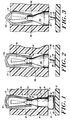
- FIG. 1 there is shown in cutaway elevation view a portion of a leadless component socket constructed and operative in accordance with the invention.
- the socket body 10 is of plate-like configuration, having flat top and bottom surfaces 12 and 14, respectively, and an array of openings 16 in a pattern providing the intended contact pattern to accommodate a matable, lead-less component or device, such as a leadless chip carrier.
- One opening is shown in Fig. 1 and is of stepped configuration, having a larger diameter portion 18 terminating at the top surface 12 and a smaller diameter section 20 terminating at the bottom surface 14.
- the first element 22 of the spring contact assembly has a central section 24 of diameter to fit within opening 20, an enlarged portion 26 of diameter larger than the diameter of section 20 and disposed in engagement with the bottom surface 14.
- the outer end of section 26 is of conical configuration 28 for mating with a contact pad 30 of a circuit board 33 or other mounting surface.
- the inner end of element 22 includes an inwardly tapering, conical surface 32, which joins an outwardly tapering end section 34.
- the second element 36 of the spring contact assembly includes a plurality of spring fingers 38 which inwardly taper, as illustrated, and which surround the end section 34 of element 22, and which are retained by the outward taper of that end section.
- the outer end of element 36 extends above top surface 12 and includes a conical surface 40, which provides a contact tip for engagement with a confronting terminal of the leadless device. Downward force on contact tip 40 causes the spring fingers 38 to ride along conical surface 32 and to produce an upwardly biased spring force for maintaining proper contact engagement between element 36 and the confronting device terminal.
- FIG. 2 An alternative embodiment is shown in Fig. 2.
- the element 24a is loosely captured on element 36a, and this assembly is loosely retained within the opening 16a of circuit board 12a by retention ring 50 provided in opening 16a.
- the ring is of a diameter to prevent removal of the assembled spring contact from either the top or the bottom of the opening.
- the element 24a has a solder terminal 52 extending outward from the bottom surface 14a of the circuit board.
- the leads 52 are aligned with the contact pads 56 on the circuit board surface, and a downward force is applied to the contact tip 40a to press the lead 52 against the contact pad 56 during soldering of the lead.
- the solder joint 58 formed between the lead and contact pad retains the socket in place and provides electrical connection between the socket leads and underlying circuit board. Loading of the spring contacts during soldering of the socket accommodates for uneven surfaces or misalignment which may be present between the socket leads and mounting surface.
- FIG. 3 A further embodiment is shown in Fig. 3.
- the top end of the mounting opening 16b has a peripheral lip 60 with an inner surface 62 which conforms to and engages a confronting portion of the spring contact tip 40b.
- the element 24b includes a cylindrical portion 64 which is in interference fit with the opening 16b for retention of element 24b in the mounting opening.
- the spring contact is preloaded when assembled in the board by reason of the bias force caused by the spring fingers 38a engaging conical surface 32a. The preloading of the contact assembly maintains sealed top and bottom surfaces of the socket body, and also provides more uniform loading of the contact array by providing an initial minimum bias force on the array of spring contacts.
- a lead 52a outwardly extends from the bottom end, and functions like in the Fig. 2 version to contact pad 56.
- FIG. 4 A variation of this embodiment is shown in Fig. 4 wherein the contact tip 40c is of conical configuration, and having a surface portion conforming to and engageable with conical surface 66 of the socket body.
- the element 24c is retained in the opening 16c by cylindrical portion 64a which has a barbed ridge 68 to anchor the element 24c in place.
- a lead 70 extends from the socket, this lead being of a form to be inserted into an opening of a circuit board on which the socket is mounted.
- FIG. 5 A further embodiment is shown in Fig. 5.
- the element 38a is substantially as shown in Fig. 4.
- the element 64b is not locked into the mounting opening as in the Fig. 4 embodiment, but is slidably disposed in the mounting opening and retained therein by a flexible film 71 mounted to the bottom surface of the body 10.
- a lead post 70a extends through an opening in film 71 to engage a confronting contacting pad 56a.
- a downward force on contact tip 40d causes the spring fingers to ride along conical surface 24d to produce a force on the contact pad 56a.
- the spring contact assembly is free-floating within its mounting opening in the absence of downward pressure on the contact tip.
- the contact tips of the spring contact assembly can take a variety of forms to suit particular requirements.
- the leads of the contact assembly for mounting the socket to a mounting surface can also take a variety of forms to suit the intended mounting arrangement.
- the leadless device socket is shown in its overall configuration in Figs. 6 and 7.
- the spring contacts are arranged within respective openings 16 in an array conforming to the terminal pattern of a device retained on the socket.
- a cover 80 Fig. 8, is employed to retain the device in the socket and in engagement with the electrical contacts.
- the cover includes mounting tabs 82 which are pivotally attached to respective posts 84 of the socket body, latch ends 86 cooperative with the body for securing the cover in a closed position, and spring fingers 88 for biasing the component onto the contact tips of the spring assemblies.
Landscapes
- Engineering & Computer Science (AREA)
- Microelectronics & Electronic Packaging (AREA)
- Connecting Device With Holders (AREA)
- Connections By Means Of Piercing Elements, Nuts, Or Screws (AREA)
- Coupling Device And Connection With Printed Circuit (AREA)
Description
- This invention relates to electronic sockets and, more particularly, to electronic component sockets for receiving leadless components.
- Electronic component sockets are known for retaining leadless components. Generally, such sockets include an array of resilient contacts in a predetermined pattern corresponding to the terminal pattern of the component or device to be mounted on the socket, and means for retaining the leadless component in position with the component terminals mated with the socket contacts.
- A novel test probe is the subject of U.S. Patent No. 4,636,026 and which provides a simple and efficient two-piece, spring-loaded contact. It is an object of this invention to provide a leadless component carrier of improved construction and operation utilizing spring contacts of the type shown in U.S. Patent No. 4,636,026.
- U.S. Patent No. 4 620 761 discloses a high density chip socket whose contact elements are in the form of coil springs retained in respective receptacles and prolonged at one end by a tail portion depending from one side of the socket body for engagement with a circuit board, while the other end of the spring is configured to contact with pads connecting with the IC chip.
- The leadless component socket in accordance with the invention comprises a socket body of electrically insulative material and having planar, substantially parallel top and bottom surfaces, and a plurality of openings between the surfaces in an array to provide an intended contact pattern. According to the invention, a two-piece spring contact assembly is retained in respective openings, with one element retained within the opening and having an outwardly extending lead for soldering or other connection to a circuit board on which the socket is mounted, and the other element extending above the upper socket surface in a position to engage the confronting terminals of a leadless component or device, such as a leadless chip carrier.
- In one embodiment, the two-piece spring contact is loosely retained within its mounting opening by cooperative means within the socket opening, such that, when the socket is mounted to a circuit board, the contact assembly can be pressed downward into engagement with the underlying circuit board and the spring contact lead then soldered into place. This mounting technique accommodates for uneven surface alignment or lack of coplanarity between the socket and circuit board surfaces. In another embodiment, one spring contact element is retained in the socket opening by interference fit. The spring contacts can be preloaded within the socket openings to provide more uniform loading across the contact array.
- The invention will be more fully understood from the following detailed description taken in conjunction with the accompanying drawings in which :
- Fig. 1 is a cutaway elevation view of one embodiment of the invention ;
- Fig. 2 is a cutaway elevation view of a second embodiment of the invention ;
- Fig. 3 is a sectional elevation view of a further embodiment of the invention ;
- Fig. 4 is a sectional elevation view of an embodiment similar to that of Fig. 3 ;
- Fig. 5 is a sectional elevation view of another embodiment of the invention ;
- Fig. 6 is a plan view of a leadless device socket in which the invention can be embodied ;
- Fig. 7 is a sectional elevation view of the socket of Fig. 6; and
- Fig. 8 is a perspective view of a cover used with the socket of Figs. 6 and 7.
- Referring to Fig. 1, there is shown in cutaway elevation view a portion of a leadless component socket constructed and operative in accordance with the invention. The
socket body 10 is of plate-like configuration, having flat top andbottom surfaces openings 16 in a pattern providing the intended contact pattern to accommodate a matable, lead-less component or device, such as a leadless chip carrier. One opening is shown in Fig. 1 and is of stepped configuration, having alarger diameter portion 18 terminating at thetop surface 12 and asmaller diameter section 20 terminating at thebottom surface 14. Thefirst element 22 of the spring contact assembly has acentral section 24 of diameter to fit withinopening 20, an enlargedportion 26 of diameter larger than the diameter ofsection 20 and disposed in engagement with thebottom surface 14. The outer end ofsection 26 is ofconical configuration 28 for mating with acontact pad 30 of a circuit board 33 or other mounting surface. The inner end ofelement 22 includes an inwardly tapering, conical surface 32, which joins an outwardly taperingend section 34. - The
second element 36 of the spring contact assembly includes a plurality ofspring fingers 38 which inwardly taper, as illustrated, and which surround theend section 34 ofelement 22, and which are retained by the outward taper of that end section. The outer end ofelement 36 extends abovetop surface 12 and includes aconical surface 40, which provides a contact tip for engagement with a confronting terminal of the leadless device. Downward force oncontact tip 40 causes thespring fingers 38 to ride along conical surface 32 and to produce an upwardly biased spring force for maintaining proper contact engagement betweenelement 36 and the confronting device terminal. - An alternative embodiment is shown in Fig. 2. The
element 24a is loosely captured on element 36a, and this assembly is loosely retained within the opening 16a ofcircuit board 12a byretention ring 50 provided in opening 16a. The ring is of a diameter to prevent removal of the assembled spring contact from either the top or the bottom of the opening. Theelement 24a has asolder terminal 52 extending outward from the bottom surface 14a of the circuit board. - To mount the socket on a
circuit board 54, theleads 52 are aligned with thecontact pads 56 on the circuit board surface, and a downward force is applied to thecontact tip 40a to press thelead 52 against thecontact pad 56 during soldering of the lead. Thesolder joint 58 formed between the lead and contact pad retains the socket in place and provides electrical connection between the socket leads and underlying circuit board. Loading of the spring contacts during soldering of the socket accommodates for uneven surfaces or misalignment which may be present between the socket leads and mounting surface. - A further embodiment is shown in Fig. 3. Here the top end of the mounting opening 16b has a
peripheral lip 60 with aninner surface 62 which conforms to and engages a confronting portion of thespring contact tip 40b. The element 24b includes acylindrical portion 64 which is in interference fit with the opening 16b for retention of element 24b in the mounting opening. The spring contact is preloaded when assembled in the board by reason of the bias force caused by thespring fingers 38a engaging conical surface 32a. The preloading of the contact assembly maintains sealed top and bottom surfaces of the socket body, and also provides more uniform loading of the contact array by providing an initial minimum bias force on the array of spring contacts. Alead 52a outwardly extends from the bottom end, and functions like in the Fig. 2 version to contactpad 56. - A variation of this embodiment is shown in Fig. 4 wherein the
contact tip 40c is of conical configuration, and having a surface portion conforming to and engageable with conical surface 66 of the socket body. Theelement 24c is retained in the opening 16c bycylindrical portion 64a which has abarbed ridge 68 to anchor theelement 24c in place. Alead 70 extends from the socket, this lead being of a form to be inserted into an opening of a circuit board on which the socket is mounted. - A further embodiment is shown in Fig. 5. The
element 38a is substantially as shown in Fig. 4. Theelement 64b is not locked into the mounting opening as in the Fig. 4 embodiment, but is slidably disposed in the mounting opening and retained therein by aflexible film 71 mounted to the bottom surface of thebody 10. Alead post 70a extends through an opening infilm 71 to engage a confronting contactingpad 56a. In use, a downward force oncontact tip 40d causes the spring fingers to ride along conical surface 24d to produce a force on thecontact pad 56a. In this embodiment the spring contact assembly is free-floating within its mounting opening in the absence of downward pressure on the contact tip. In the presence of such downward pressure the spring assembly is urged downward to provide pressure contact between thelead 70a andcontact pad 56a, and between thecontact tip 40d and the contact pad of an electronic component mounted on the assembly. This version allows for relative ease of alignment between the spring contact assembly and the underlying contact pads, since there is only loose engagement therebetween until pressure is applied to the contact tip during use. - The contact tips of the spring contact assembly can take a variety of forms to suit particular requirements. The leads of the contact assembly for mounting the socket to a mounting surface can also take a variety of forms to suit the intended mounting arrangement.
- The leadless device socket is shown in its overall configuration in Figs. 6 and 7. The spring contacts are arranged within
respective openings 16 in an array conforming to the terminal pattern of a device retained on the socket. Acover 80, Fig. 8, is employed to retain the device in the socket and in engagement with the electrical contacts. The cover includesmounting tabs 82 which are pivotally attached torespective posts 84 of the socket body, latch ends 86 cooperative with the body for securing the cover in a closed position, andspring fingers 88 for biasing the component onto the contact tips of the spring assemblies.
Claims (10)
- A leadless component socket comprising :
a socket body (10) of electrically insulative material having a planar top surface (12) and a substantially parallel planar bottom surface (14;14a) and a plurality of openings(16; 16a; 16b; 16c) between the top and bottom surfaces in an array to provide an intended contact pattern ;
a plurality of spring contact assemblies each retained in a respective opening, each spring contact assembly including :
a first element (22) disposed within the opening (20) adjacent the bottom surface of the socket body and having an outwardly extending lead (26;52;52a;70;70a) for attachment to a contact element (30;56,56a) of a mounting member (33);
a second element (36) disposed within the opening adjacent the top surface of the socket body and having a contact tip (40;40a;40b;40c) outwardly extending from the top surface for engaging a contact of a leadless component mounted on the socket ;
one of the elements having a ramp surface (32) ;
the other one of the elements having spring means (38,38a) cooperative with the ramp surface, the spring means being movable in a direction transverse to the axis of the first element and operative to bias the first element to a normally outward axial position. - The invention of claim 1 wherein the openings (16) in the socket body are of stepped configuration having a larger diameter portion (18) terminating at the top surface (12) and a smaller diameter portion (20) terminating at the bottom surface (14) ; the first element (22) of the spring contact assembly having a central section (24) fitted within the smaller diameter portion (20).
- The invention of claim 1 wherein the first element (22) of the spring contact assembly has an outwardly extending lead (26) which includes a distal end (28) of generally conical configuration for mating with the contact element (30) of a mounting member (33).
- The invention of claim 1 wherein the socket body includes a plurality of openings (16;16a;16b;16c) each having retention means therein; each of the spring contact assemblies (22,36) being loosely retained within respective openings by said retaining means.
- The invention of claim 4 wherein the retaining means includes for each of said openings a retention ring (50) within the opening disposed intermediate the top and bottom surfaces (12,14) and sized to prevent removal of the assembled spring contact assembly from the top and bottom of the opening.
- The invention of claim 1 wherein each of the plurality of openings in the socket body include a peripheral lip (60) operative to engage a confronting portion of the spring contact tip (40b) of the second element of the spring contact assembly for retention of the element in the mounting opening.
- The invention of claim 6 wherein the first element (22) is secured within the mounting opening and operative to provide a preloading force on the second element(36).
- The invention of claim 1 wherein the plurality of openings (16) in the socket body each includes a peripheral lip at the top surface operative to engage the second element of the spring assembly for retention of the second element in the mounting opening ;
a flexible film (71) provided on the bottom surface and having an opening aligned with the mounting opening ;
the outwardly extending lead (70a) of the first element of the spring contact assembly extending through the opening in the flexible film for engagement with a contact element (56a) of a mounting member. - The invention of claim 1 including means for retaining the spring contact assemblies in the respective openings of the socket body.
- The invention of claim 1 including cover means (80) attached to the socket body and operative to maintain a component on the socket body in engagement with the contact tips (40d) of the spring contact assemblies.
Applications Claiming Priority (2)
| Application Number | Priority Date | Filing Date | Title |
|---|---|---|---|
| US07/115,511 US4838801A (en) | 1987-11-02 | 1987-11-02 | Leadless component socket |
| US115511 | 1987-11-02 |
Publications (2)
| Publication Number | Publication Date |
|---|---|
| EP0317384A1 EP0317384A1 (en) | 1989-05-24 |
| EP0317384B1 true EP0317384B1 (en) | 1994-01-05 |
Family
ID=22361875
Family Applications (1)
| Application Number | Title | Priority Date | Filing Date |
|---|---|---|---|
| EP88402700A Expired - Lifetime EP0317384B1 (en) | 1987-11-02 | 1988-10-26 | Leadless component socket |
Country Status (5)
| Country | Link |
|---|---|
| US (1) | US4838801A (en) |
| EP (1) | EP0317384B1 (en) |
| JP (1) | JPH071707B2 (en) |
| CA (1) | CA1294679C (en) |
| DE (1) | DE3886902T2 (en) |
Families Citing this family (25)
| Publication number | Priority date | Publication date | Assignee | Title |
|---|---|---|---|---|
| US5205739A (en) * | 1989-11-13 | 1993-04-27 | Augat Inc. | High density parallel interconnect |
| JPH07120545B2 (en) * | 1991-03-27 | 1995-12-20 | 山一電機株式会社 | Nested pressure connector |
| US5167512A (en) * | 1991-07-05 | 1992-12-01 | Walkup William B | Multi-chip module connector element and system |
| US5205742A (en) * | 1991-08-22 | 1993-04-27 | Augat Inc. | High density grid array test socket |
| US5215472A (en) * | 1991-08-22 | 1993-06-01 | Augat Inc. | High density grid array socket |
| US5221209A (en) * | 1991-08-22 | 1993-06-22 | Augat Inc. | Modular pad array interface |
| US5199889A (en) * | 1991-11-12 | 1993-04-06 | Jem Tech | Leadless grid array socket |
| JPH05182729A (en) * | 1991-12-26 | 1993-07-23 | Yamaichi Electron Co Ltd | Contactor for electrical parts |
| JPH0641149U (en) * | 1992-10-23 | 1994-05-31 | 株式会社エンプラス | IC socket |
| US5469074A (en) * | 1994-02-08 | 1995-11-21 | The Whitaker Corporation | Chip socket testing apparatus with adjustable contact force |
| US5742481A (en) * | 1995-10-04 | 1998-04-21 | Advanced Interconnections Corporation | Removable terminal support member for integrated circuit socket/adapter assemblies |
| JP2000323241A (en) * | 1999-05-12 | 2000-11-24 | Honda Tsushin Kogyo Co Ltd | connector |
| JP3768183B2 (en) * | 2002-10-28 | 2006-04-19 | 山一電機株式会社 | IC socket for narrow pitch IC package |
| TWM289241U (en) * | 2005-10-07 | 2006-04-01 | Lotes Co Ltd | Electric connector |
| US7097485B1 (en) * | 2005-12-02 | 2006-08-29 | Advanced Connection Technology Inc. | Electrical connector having resilient conductive terminals |
| US7554800B2 (en) * | 2006-06-05 | 2009-06-30 | Vulcan Portals, Inc. | External module electrical and mechanical attachment mechanism and method |
| US7794237B1 (en) * | 2009-08-21 | 2010-09-14 | Hon Hai Precision Ind. Co., Ltd. | Electrical connector having improved retaining arrangement between the housing and the contacts |
| US7927109B1 (en) | 2009-10-30 | 2011-04-19 | Hon Hai Precision Ind. Co., Ltd. | Electrical connector having plated conductive layer |
| US8147253B2 (en) | 2010-06-30 | 2012-04-03 | Advanced Interconnections Corp. | Split ring terminal assembly |
| US8210855B1 (en) * | 2011-03-11 | 2012-07-03 | Cheng Uei Precision Industry Co., Ltd. | Electrical connector |
| JP5762902B2 (en) * | 2011-09-16 | 2015-08-12 | 日本発條株式会社 | Contact terminal |
| MY168237A (en) * | 2012-10-12 | 2018-10-15 | Jf Microtechnology Sdn Bhd | Ground contact of an integrated circuit testing apparatus |
| JP6107144B2 (en) * | 2013-01-09 | 2017-04-05 | 株式会社ソシオネクスト | Contactor |
| US9172160B2 (en) | 2013-03-13 | 2015-10-27 | Intel Corporation | Vertical socket contact with flat force response |
| KR101869211B1 (en) * | 2014-08-08 | 2018-06-19 | 니혼 하츠쵸 가부시키가이샤 | Connecting terminal |
Family Cites Families (10)
| Publication number | Priority date | Publication date | Assignee | Title |
|---|---|---|---|---|
| US4083623A (en) * | 1977-02-18 | 1978-04-11 | Amp Incorporated | Mini spring socket with plastic base |
| US4373778A (en) * | 1980-12-30 | 1983-02-15 | International Business Machines Corporation | Connector implemented with fiber optic means and site therein for integrated circuit chips |
| JPS5958850A (en) * | 1982-09-29 | 1984-04-04 | Fujitsu Ltd | Integrated circuit socket |
| DE3421799A1 (en) * | 1984-06-12 | 1985-12-12 | Feinmetall Gmbh, 7033 Herrenberg | CONTACT ELEMENT FOR TEST ADAPTER |
| IT1179206B (en) * | 1984-06-13 | 1987-09-16 | Texas Instruments Italia Spa | ELECTRIC CONNECTOR AND ITS MANUFACTURING PROCESS |
| US4620761A (en) * | 1985-01-30 | 1986-11-04 | Texas Instruments Incorporated | High density chip socket |
| US4667154A (en) * | 1985-06-26 | 1987-05-19 | Lehighton Electronics, Inc. | Electrical contact assembly |
| US4645278A (en) * | 1985-09-09 | 1987-02-24 | Texas Instruments Incorporated | Circuit panel connector, panel system using the connector, and method for making the panel system |
| US4716365A (en) * | 1985-10-11 | 1987-12-29 | Lisle Corporation | Circuit tester |
| US4636026A (en) * | 1985-12-20 | 1987-01-13 | Augat Inc. | Electrical test probe |
-
1987
- 1987-11-02 US US07/115,511 patent/US4838801A/en not_active Expired - Lifetime
-
1988
- 1988-10-26 EP EP88402700A patent/EP0317384B1/en not_active Expired - Lifetime
- 1988-10-26 DE DE3886902T patent/DE3886902T2/en not_active Expired - Fee Related
- 1988-11-01 CA CA000581825A patent/CA1294679C/en not_active Expired - Fee Related
- 1988-11-02 JP JP63278506A patent/JPH071707B2/en not_active Expired - Lifetime
Non-Patent Citations (1)
| Title |
|---|
| ELECTRONICS, vol. 59, no. 21, May 1986, pages 24 - 27; New York, US; J. LYMAN: "How Surface Mounting Is Changing Interconnection" * |
Also Published As
| Publication number | Publication date |
|---|---|
| US4838801A (en) | 1989-06-13 |
| JPH071707B2 (en) | 1995-01-11 |
| DE3886902D1 (en) | 1994-02-17 |
| DE3886902T2 (en) | 1994-05-19 |
| CA1294679C (en) | 1992-01-21 |
| JPH01154478A (en) | 1989-06-16 |
| EP0317384A1 (en) | 1989-05-24 |
Similar Documents
| Publication | Publication Date | Title |
|---|---|---|
| US4838801A (en) | Leadless component socket | |
| EP0780028B1 (en) | Ball grid array socket | |
| EP1029386B1 (en) | Converter socket terminal | |
| US4682829A (en) | Surface mount socket for dual in-line package | |
| US6431915B1 (en) | RF cable connector assembly for preventing mis-mating | |
| KR100371660B1 (en) | IC Socket | |
| US5362244A (en) | Socket having resilient locking tabs | |
| US5022871A (en) | Multipolar connector socket | |
| US7794237B1 (en) | Electrical connector having improved retaining arrangement between the housing and the contacts | |
| EP0664581A2 (en) | Low profile board to board connector | |
| US7553202B2 (en) | Electrical terminal | |
| CA2176785A1 (en) | Terminal socket assembly | |
| US5603620A (en) | Integrated printed circuit connector and ground clip assembly | |
| US20040023527A1 (en) | Module connector | |
| JPS61271765A (en) | Electric connector | |
| EP0724304B1 (en) | Battery terminal of miniature electronic apparatus and structure for retaining the same | |
| US6731516B1 (en) | Land grid array connector having movable engagement of electrical contacts thereinto | |
| US5009606A (en) | Separable electrical connector | |
| US6644985B2 (en) | Ball attached zero insertion force socket | |
| US20070281515A1 (en) | Electrical connector with movable contact | |
| WO1986007204A1 (en) | Surface mount electrical connector with floating electrical terminals | |
| US4638406A (en) | Discrete component mounting assembly | |
| US4832611A (en) | Electrical connector comprising combination of individual mating and pin elements as a contact member | |
| US20060121751A1 (en) | LGA socket connector with floating cover | |
| US4681391A (en) | Electric connector |
Legal Events
| Date | Code | Title | Description |
|---|---|---|---|
| PUAI | Public reference made under article 153(3) epc to a published international application that has entered the european phase |
Free format text: ORIGINAL CODE: 0009012 |
|
| AK | Designated contracting states |
Kind code of ref document: A1 Designated state(s): DE FR GB |
|
| 17P | Request for examination filed |
Effective date: 19891115 |
|
| 17Q | First examination report despatched |
Effective date: 19920120 |
|
| GRAA | (expected) grant |
Free format text: ORIGINAL CODE: 0009210 |
|
| AK | Designated contracting states |
Kind code of ref document: B1 Designated state(s): DE FR GB |
|
| REF | Corresponds to: |
Ref document number: 3886902 Country of ref document: DE Date of ref document: 19940217 |
|
| ET | Fr: translation filed | ||
| PG25 | Lapsed in a contracting state [announced via postgrant information from national office to epo] |
Ref country code: GB Effective date: 19941026 |
|
| PLBE | No opposition filed within time limit |
Free format text: ORIGINAL CODE: 0009261 |
|
| STAA | Information on the status of an ep patent application or granted ep patent |
Free format text: STATUS: NO OPPOSITION FILED WITHIN TIME LIMIT |
|
| 26N | No opposition filed | ||
| GBPC | Gb: european patent ceased through non-payment of renewal fee |
Effective date: 19941026 |
|
| PG25 | Lapsed in a contracting state [announced via postgrant information from national office to epo] |
Ref country code: FR Effective date: 19950630 |
|
| PG25 | Lapsed in a contracting state [announced via postgrant information from national office to epo] |
Ref country code: DE Effective date: 19950701 |
|
| REG | Reference to a national code |
Ref country code: FR Ref legal event code: ST |