EP0315275A2 - Microcalculateur avec des circuits intégrés flexibles et spécifiques pour l'application - Google Patents
Microcalculateur avec des circuits intégrés flexibles et spécifiques pour l'application Download PDFInfo
- Publication number
- EP0315275A2 EP0315275A2 EP88202444A EP88202444A EP0315275A2 EP 0315275 A2 EP0315275 A2 EP 0315275A2 EP 88202444 A EP88202444 A EP 88202444A EP 88202444 A EP88202444 A EP 88202444A EP 0315275 A2 EP0315275 A2 EP 0315275A2
- Authority
- EP
- European Patent Office
- Prior art keywords
- memory
- data
- address
- macroinstructions
- register
- Prior art date
- Legal status (The legal status is an assumption and is not a legal conclusion. Google has not performed a legal analysis and makes no representation as to the accuracy of the status listed.)
- Granted
Links
- 230000006870 function Effects 0.000 claims abstract description 18
- 238000012360 testing method Methods 0.000 claims abstract description 14
- 238000012545 processing Methods 0.000 claims abstract description 8
- 239000000758 substrate Substances 0.000 claims description 14
- 238000013507 mapping Methods 0.000 claims description 7
- 238000012163 sequencing technique Methods 0.000 claims description 4
- 230000002457 bidirectional effect Effects 0.000 claims description 2
- 230000005540 biological transmission Effects 0.000 claims 1
- 230000008878 coupling Effects 0.000 claims 1
- 238000010168 coupling process Methods 0.000 claims 1
- 238000005859 coupling reaction Methods 0.000 claims 1
- 238000007792 addition Methods 0.000 abstract description 6
- 238000012217 deletion Methods 0.000 abstract description 2
- 230000037430 deletion Effects 0.000 abstract description 2
- 238000012986 modification Methods 0.000 abstract description 2
- 230000004048 modification Effects 0.000 abstract description 2
- 230000007246 mechanism Effects 0.000 description 16
- 238000000034 method Methods 0.000 description 9
- 238000013461 design Methods 0.000 description 4
- 238000013459 approach Methods 0.000 description 2
- 230000008859 change Effects 0.000 description 2
- XUIMIQQOPSSXEZ-UHFFFAOYSA-N Silicon Chemical compound [Si] XUIMIQQOPSSXEZ-UHFFFAOYSA-N 0.000 description 1
- 230000009471 action Effects 0.000 description 1
- 230000008901 benefit Effects 0.000 description 1
- 230000015572 biosynthetic process Effects 0.000 description 1
- 239000000872 buffer Substances 0.000 description 1
- 238000004364 calculation method Methods 0.000 description 1
- 238000004590 computer program Methods 0.000 description 1
- 239000012141 concentrate Substances 0.000 description 1
- 230000001419 dependent effect Effects 0.000 description 1
- 238000012938 design process Methods 0.000 description 1
- 238000010586 diagram Methods 0.000 description 1
- 238000006073 displacement reaction Methods 0.000 description 1
- 239000003292 glue Substances 0.000 description 1
- 230000002093 peripheral effect Effects 0.000 description 1
- 230000008569 process Effects 0.000 description 1
- 229910052710 silicon Inorganic materials 0.000 description 1
- 239000010703 silicon Substances 0.000 description 1
- 238000003786 synthesis reaction Methods 0.000 description 1
Images
Classifications
-
- G—PHYSICS
- G06—COMPUTING; CALCULATING OR COUNTING
- G06F—ELECTRIC DIGITAL DATA PROCESSING
- G06F13/00—Interconnection of, or transfer of information or other signals between, memories, input/output devices or central processing units
-
- G—PHYSICS
- G06—COMPUTING; CALCULATING OR COUNTING
- G06F—ELECTRIC DIGITAL DATA PROCESSING
- G06F11/00—Error detection; Error correction; Monitoring
- G06F11/22—Detection or location of defective computer hardware by testing during standby operation or during idle time, e.g. start-up testing
- G06F11/2205—Detection or location of defective computer hardware by testing during standby operation or during idle time, e.g. start-up testing using arrangements specific to the hardware being tested
- G06F11/2236—Detection or location of defective computer hardware by testing during standby operation or during idle time, e.g. start-up testing using arrangements specific to the hardware being tested to test CPU or processors
-
- G—PHYSICS
- G06—COMPUTING; CALCULATING OR COUNTING
- G06F—ELECTRIC DIGITAL DATA PROCESSING
- G06F15/00—Digital computers in general; Data processing equipment in general
- G06F15/76—Architectures of general purpose stored program computers
- G06F15/78—Architectures of general purpose stored program computers comprising a single central processing unit
- G06F15/7867—Architectures of general purpose stored program computers comprising a single central processing unit with reconfigurable architecture
-
- G—PHYSICS
- G06—COMPUTING; CALCULATING OR COUNTING
- G06F—ELECTRIC DIGITAL DATA PROCESSING
- G06F9/00—Arrangements for program control, e.g. control units
- G06F9/06—Arrangements for program control, e.g. control units using stored programs, i.e. using an internal store of processing equipment to receive or retain programs
- G06F9/22—Microcontrol or microprogram arrangements
- G06F9/26—Address formation of the next micro-instruction ; Microprogram storage or retrieval arrangements
- G06F9/261—Microinstruction address formation
-
- G—PHYSICS
- G06—COMPUTING; CALCULATING OR COUNTING
- G06F—ELECTRIC DIGITAL DATA PROCESSING
- G06F9/00—Arrangements for program control, e.g. control units
- G06F9/06—Arrangements for program control, e.g. control units using stored programs, i.e. using an internal store of processing equipment to receive or retain programs
- G06F9/22—Microcontrol or microprogram arrangements
- G06F9/26—Address formation of the next micro-instruction ; Microprogram storage or retrieval arrangements
- G06F9/262—Arrangements for next microinstruction selection
- G06F9/264—Microinstruction selection based on results of processing
- G06F9/265—Microinstruction selection based on results of processing by address selection on input of storage
-
- G—PHYSICS
- G06—COMPUTING; CALCULATING OR COUNTING
- G06F—ELECTRIC DIGITAL DATA PROCESSING
- G06F9/00—Arrangements for program control, e.g. control units
- G06F9/06—Arrangements for program control, e.g. control units using stored programs, i.e. using an internal store of processing equipment to receive or retain programs
- G06F9/30—Arrangements for executing machine instructions, e.g. instruction decode
- G06F9/30145—Instruction analysis, e.g. decoding, instruction word fields
-
- G—PHYSICS
- G11—INFORMATION STORAGE
- G11C—STATIC STORES
- G11C29/00—Checking stores for correct operation ; Subsequent repair; Testing stores during standby or offline operation
- G11C29/04—Detection or location of defective memory elements, e.g. cell constructio details, timing of test signals
- G11C29/08—Functional testing, e.g. testing during refresh, power-on self testing [POST] or distributed testing
- G11C29/12—Built-in arrangements for testing, e.g. built-in self testing [BIST] or interconnection details
- G11C29/14—Implementation of control logic, e.g. test mode decoders
- G11C29/16—Implementation of control logic, e.g. test mode decoders using microprogrammed units, e.g. state machines
Definitions
- This invention relates to the field of digital microcomputers embodied in a single integrated circuit.
- microcomputers which include, in one integrated circuit, RAM and various dedicated functions, in addition to the central processing unit itself
- RAM random access memory
- various dedicated functions in addition to the central processing unit itself
- the process of designing such devices has been geared toward producing standard off-the-shelf products which generally meet the public's needs.
- the architectures underlying such devices have not been designed to be customized to fit the needs of particular users. Rather, they have been designed to perform optimally for a predetermined set of macroinstructions.
- microcomputers examples include the Intel 8031/8051, the architecture of which is specified in Chapter 6 of the 1984 Intel Microcontroller Handbook (Order No. 210918-002), and the Programmable Single Chip MOS Computer disclosed in U.S. Pat. Nos. 4,153,933 and 4,306,163. From what one can discern from the descriptions of these devices (and all other microcomputer architectures known to the inventors), it is clear that their architectures are rigid and inflexible. Memory sizes for code and data, macroinstruction decoding and timing, and even the available peripheral functions (such as timers/counters and serial controllers), are all predetermined and not capable of change.
- microcomputer user is concerned only with its external interface -- e.g. , the macroinstruction set and pin definitions, perhaps including the timing required to execute each instruction.
- the user is concerned only with which operations the chip performs, not how it performs those operations.
- microcomputer architectures consist of minimized logic paths designed to optimize the performance of the device for its predetermined functions.
- the microarchitecture is designed with one purpose in mind -- executing the specified instruction set as quickly as possible for a given integrated circuit area. No thought is given to the possibility that the same architecture might be reused for a slightly (or perhaps significantly different) application.
- An additional problem relates to the testing of that on-chip memory independently from the CPU.
- an entire microcomputer including memory
- What this invention provides is a general purpose microcomputer architecture that is flexible enough to permit individual users to specify, for example, changes in the definition of macroinstructions, or simply execution timing, as well as the size of on-board memory (whether for data or code). Each user can specify his or her own custom, dedicated logic functions, and have such functions easily incorporated into the macroinstruction set through the internal microcomputer architecture.
- these functions are incorporated into the microarchitecture by also providing means for adding the registers associated with these dedicated functions to the internal register file of the microcomputer.
- This approach provides significantly greater flexibility, enabling the user to manipulate that custom external device as if it were incorporated within the microarchitecture itself.
- the user need not specify fixed external memory locations (requiring the reading and writing of values into other scarce internal registers) to perform simple logical and arithmetic operations. The user thus achieves savings in space and performance as well as in the cost of program design.
- FASMIC architecture Another problem addressed by the FASMIC architecture relates to the testing of on-chip memory independently from the CPU.
- This invention provides a mechanism for testing on-chip memory, independent of the internal bus (and thus the rest of the integrated circuit), thereby providing a solution which utilizes standard memory addressing logic and avoids the significant extra cost of designing dedicated logic, particularly where variable memory sizes are permitted (according to each user's individual requirements).
- the mechanism itself incorporates "scan path circuitry" which has been published in another context. See the LSA2001 Silicon-Gate HCMOS Structured Array data sheet, pp. 8-10, published by LSI Logic Corporation in March, 1987 (explained in detail below).
- This "scan" mechanism has never before been utilized, however, in the context of a microcomputer, in which the testing of memory independently from the main internal bus (and thus the rest of the CPU) is of great significance.
- this invention comprises a digital computer on a single substrate, comprising a bidirectional data bus, memory for the storage of data or code, said memory comprising one or more registers used for the temporary storage of data during the operation of said digital computer, means for addressing said memory, said addressing means comprising means for including the addresses of external device registers, not located on said substrate, within the same address space used for said memory, said means permitting the same degree of direct manipulation of said external registers as is permitted registers located on said substrate, and a central processing unit which interprets and executes macroinstructions, and which performs arithmetic and logical operations, said central processing unit coupled to said data bus, to said memory and to said addressing means, said central processing unit comprising a microengine for controlling the operation of said computer, said microengine comprising macroinstruction memory for storing one or more of the macroinstructions to be executed by said computer, microcode memory, said microcode memory comprising one or more microinstructions, each of said microinstructions comprising one or more control
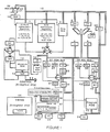
- This invention is embodied in the architecture of the Flexible ASIC Microcomputer (“FASMIC") illustrated in Figure 1. Included are two distinct sets of register blocks, the first block 1 of registers being both bit-addressable and byte-addressable, and the second block 2 of registers being only byte-addressable. Although these registers are illustrated in two distinct blocks in Figure 1, the registers in both sets are physically located throughout the architecture of this chip (also illustrated in this diagram). The purpose of grouping these registers in blocks 1 and 2 is simply to illustrate the appropriate addressing mechanism associated with each register.
- FASMIC Flexible ASIC Microcomputer
- registers in blocks 1 and 2 are accessible both internally, via microcode, and externally, via user macroinstructions.
- the user is also provided with a set of general purpose registers, included in "scratchpad" Data RAM 3.
- registers A and B are also shown below the ALU 6, which performs well-known arithmetic and logical operations.
- the two ALU operands are stored in registers TP1 7 and TP2 8, and various result flags of ALU operations are stored in PSW register 9. All special purpose registers, as well as the ALU and Data RAM 3, are accessible via the Internal Bus 10, from which information can either be read or written.
- This particular embodiment of the FASMIC architecture is controlled by a general purpose microengine, which generates control signals 11 which are distributed thoughout the integrated circuit.
- This microengine includes an instruction register (IR) 12, which initially holds each user macroinstruction after it is fetched from program memory.
- IR instruction register
- This macroinstruction is decoded via the Map ROM 13, which maps each macroinstruction into a starting address (or "entry point") in the Microcode ROM 14.
- the Map ROM simply contains a table of microinstruction entry points, and is addressed via macroinstruction opcodes.
- One or more macroinstruction opcodes yields a particular entry point of the first microinstruction in the sequence of microinstructions which interprets that group of macroinstructions.
- the functionality of both the Map ROM 13 and the Microcode ROM 14 can easily be manifested, in another embodiment, in either a PLA or purely in logic synthesis (as opposed to a ROM). As a general rule, it makes no difference to the user how this functionality is manifested, provided that the precise functionality is performed within specified size and performance boundaries.
- the FASMIC architecture is designed to permit significant flexibility by maintaining a binary representation of this functionality, thereby enabling the user to select a particular manifestation (e.g. , 64K ROM) to suit his or her individual space, performance or other requirements.
- Microinstructions Residing in the Microcode ROM are the sequences of microinstructions (described in greater detail below) which contain the control signals necessary to interpret particular macroinstructions by causing the rest of the microarchitecture to perform the appropriate functions. These control signals are organized into fields, each field representing a particular function, such as reading a particular register and placing its contents onto the internal bus. These fields are further organized into fixed-length microinstruction formats, each of which constitutes a type of microinstruction containing multiple fields of control signals. Each microinstruction is stored, immediately prior to its execution, in the micro word register (MWR) 15, from which it is decoded by additional control logic distributed throughout the integrated circuit.
- MWR micro word register
- the sequencing of microinstruction execution is controlled via MUX 16, which, as a default, simply increments the address to the next sequential microinstruction (because the sequence of microinstructions is generally known for a particular group of one or more macroinstructions).
- the sequencing is conditional -- e.g. , when a conditional microcode branch occurs. In that case, a particular field of the previous microinstruction itself contains the next address (jumped to if the condition was met).
- the next address is determined by the output of the Map ROM, because that address is dependent upon the particular macroinstruction to be executed next.
- MUX 16 determines the address of the next microinstruction to be executed by (1) incrementing the address of the previous microinstruction, (2) using the entry point address generated by the Map ROM or (3) using the branch address generated from or contained within the previous microinstruction (stored in MWR). This address is then stored in the micro address register (MAR) 17 which addresses the Microcode ROM directly, causing the microinstruction at that address to be loaded into MWR and then executed.
- MAR micro address register
- MUX 16 determines the source of the address of the next microinstruction to be executed
- MUX 18 determines the source of the encoded "address" of the register to be accessed (e.g. , when a microinstruction or a macroinstruction operates on a particular register), and then stores that encoded address in the RAM/Register Address Register (RAR) 19.
- RAR RAM/Register Address Register
- the first of the three possible sources for RAR is the Internal Bus 10, containing the absolute address of the register (or RAM location) specified by the currently executing microinstruction itself. These control signals are decoded from MWR, and then placed onto the Internal Bus where they may be used to select a particular register (or RAM location) from which data are read or into which data are written. Additional control signals will, of course, determine whether MUX 18 selects this or one of the other two sources.
- the second potential RAR source 20 is also an absolute address, but is derived not from a microinstruction, but from the currently executing macroinstruction.
- This address is composed of three components. The most significant bits of the address are fixed, indicating the particular offset in Data RAM 3 reserved for general purpose registers. The next most significant bits are determined by certain bits of the PSW, indicating which "bank" of general purpose registers in RAM is currently being accessed. Finally, certain bits of the macroinstruction itself specify which particular register in the current bank of Data RAM 3 registers is being accessed. These three components combine to form an absolute address in Data RAM 3 which, if selected on MUX 18, will be loaded into RAR and used to address the Data RAM 3 register to be accessed.
- the third possible RAR source 21 is an address in Data RAM 3 obtained through the following indirect addressing means.
- Source 20 loads the indirect address into RAR.
- the contents of RAR are then used as a pointer (the indirect address) into Data RAM 3.
- the contents of the word at this address in Data RAM 3 (the absolute address) become source 21 into MUX 18, which, if selected, is loaded into RAR.
- MUX 22 conceptually illustrates that the data in the register accessed via RAR is obtained from a special purpose bit-addressable register, a special purpose byte-addressable register or a general purpose Data RAM register.
- both microinstructions and macroinstructions can access off-chip data RAM via external port P2 23 and port P0 24.
- the stack pointer register (SP) 25 is used to implement a well-known software mechanism for organizing user memory by saving data in a "last in first out” (LIFO) manner. SP contains the address of the "top” (last in, if the stack grows upward) item on the stack.
- External port P1 26 is simply a general-purpose parallel port.
- External ports P2 23 and P0 24 are utilized to access off-chip program and data memory (RAM or ROM).
- the address (of the next macroinstruction to be executed) is sent through ports P2 and P0, and is calculated in two physically separate components -- one for the most significant half and one for the least significant half of the address. These two components of the "next macroinstruction address generation" mechanism are practically identical.
- DPH 27 and DPL 28 which contains an offset into external data RAM
- PCH 29 and PCL 30 which contains the address of the next macroinstruction
- an internal register IH 31 and IL 32
- the high component of this mechanism contains an incrementer/decrementer 33, while the low component contains simply an incrementer 34. This difference is due to the fact that the low component computes relative address displacements using the ALU, leaving only a minor increment or decrement in the high component, which is handled in hardware via incrementer/decrementer 33.
- MUX 35 and MUX 36 receive control signals that determine which of the three registers to access for generating the address. Because this calculation is often complex (requiring, for example, ALU operations), separate internal PD (program counter and data pointer) buses PDH 37 and PDL 38 are employed, to permit data to be transferred among the registers associated with this mechanism and onto the Internal Bus, from which it can be manipulated via the ALU. Buffers 39 and 40 contain the well-known logic mechanism necessary to insure that data is properly transferred between the PD buses and the Internal Bus without any conflict (because the Internal Bus can only be "mastered" by one source at any given time).
- next macroinstruction address is computed via this mechanism under microcode control (for example, by manipulating data across the PD buses and the Internal Bus, using the ALU to perform any necessary logical and arithmetic operations).
- External data RAM addresses are also computed via this mechanism.
- the address of the next macroinstruction to be executed is stored ultimately in the program address registers (PARH 41 and PARL 42).
- PARH 41 and PARL 42 program address registers
- some or all of the user's program may be stored in optional on-chip program ROM 43. In any event, this mechanism results either in the reading or writing of external data RAM, or in the fetching of the next macroinstruction (whether from external memory or on-chip ROM), which is then loaded onto the Internal Bus and into IR, whereupon it is executed by the general purpose microengine described above.
- the architecture also includes a Timing mechanism 44 and certain dedicated logic functions (Timers/Counters 45, Interrupt Mechanism 46 and Serial Controllers 47), each of which is well-known in the art and explained in detail in Chapter 6 of the 1984 Intel Microcontroller Handbook (Order No. 210918-002).
- External port P3 48 provides access to these dedicated functions, which are only tangentially related to this invention, with the exception of the addressing of the external registers of the user-specified dedicated logic functions (incorporated within the address space of the internal registers in blocks 1 and 2).
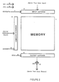
- Illustrated in Figure 2 is a separate mechanism integrated into the FASMIC architecture which enables the testing of on-chip memory without utilizing the Internal Bus. Note that, rather than designing dedicated memory address logic into the memory, this invention takes advantage of the "scan" technique referred to above, which is already designed into standard memory components.
- the Memory itself 1 is surrounded by three sets of latches (Input Latches 2, Address Latches 3 and Output Latches 4), in addition to certain control signals.
- the cell select signal (CS) 5 is reset (disabling the Memory)
- the serial address bits (addressing the data to be tested, whether read or written) may be loaded into the Address Latches (the width of which is determined by the RAM width, with one latch provided per bit), by strobing the input address clock (ICKADR) 6.
- test data may be input serially into the Input Latches (one per bit of input) by strobing the input data clock (ICKDATA) 7.
- test data already strobed into the Input Latches will be written into Memory at the addresses previously strobed into the Address Latches.
- the same procedure is followed to read test data from Memory, except that WE is reset.
- the test data is then placed at the inputs of the Output Latches, where it can be latched by strobing the output data clock (OCK) 9 once.
- Data can then be accessed serially by enabling the output (OE) 10, resetting CS (disabling the Memory) and strobing the internal scan clock until each bit of data has been shifted out.
- Memory can be tested via the scan mechanism, using only the Input, Output and Address Latches supplied with the Memory itself, thus avoiding the problems resulting from use of the Internal Bus, which would require the creation of dedicated logic.
- the additional length of this program illustrates the extra programming required each time that an external register is manipulated. If the registers of the user's device are accessed frequently, the user's program would be significantly slower, and occupy significantly more space, than the corresponding program utilizing the FASMIC method.
- this invention relieves the user of the need to handle excess "data movement” instructions (which often occupy an inordinate percentage of many computer programs), and frees the user to concentrate on the particular task at hand, requiring the use of "data manipulation” (or number-crunching) instructions.
- ADDC add with carry
- the microcode simply needs to be modified slightly. Rather than use the carry value generated by the addition operation in the ALU, the microcode simply needs to set the carry bit directly sometime after the addition operation. This slight change in operation for a particular user is possible (without any additional hardware changes) because the FASMIC architecture is designed with this flexibility in mind.
Applications Claiming Priority (2)
| Application Number | Priority Date | Filing Date | Title |
|---|---|---|---|
| US07/116,411 US4878174A (en) | 1987-11-03 | 1987-11-03 | Flexible ASIC microcomputer permitting the modular modification of dedicated functions and macroinstructions |
| US116411 | 1987-11-03 |
Publications (3)
| Publication Number | Publication Date |
|---|---|
| EP0315275A2 true EP0315275A2 (fr) | 1989-05-10 |
| EP0315275A3 EP0315275A3 (en) | 1990-08-16 |
| EP0315275B1 EP0315275B1 (fr) | 1995-04-19 |
Family
ID=22367030
Family Applications (1)
| Application Number | Title | Priority Date | Filing Date |
|---|---|---|---|
| EP88202444A Expired - Lifetime EP0315275B1 (fr) | 1987-11-03 | 1988-11-02 | Microcalculateur avec des circuits intégrés flexibles et spécifiques pour l'application |
Country Status (5)
| Country | Link |
|---|---|
| US (1) | US4878174A (fr) |
| EP (1) | EP0315275B1 (fr) |
| JP (1) | JP2651218B2 (fr) |
| KR (1) | KR890008699A (fr) |
| DE (1) | DE3853613T2 (fr) |
Cited By (26)
| Publication number | Priority date | Publication date | Assignee | Title |
|---|---|---|---|---|
| EP0532087A2 (fr) * | 1991-09-10 | 1993-03-17 | STMicroelectronics S.r.l. | Procédé de vérification de mémoires d'un microordinateur programmé au moyen d'un microprogramme incorporé dans le microordinateur lui même |
| EP0562151A1 (fr) * | 1992-03-27 | 1993-09-29 | Siemens Aktiengesellschaft | Microprocesseur intégré |
| WO1996034346A1 (fr) * | 1995-04-28 | 1996-10-31 | Xilinx, Inc. | Microprocesseur a registres repartis accessibles par logique programmable |
| US6754882B1 (en) | 2002-02-22 | 2004-06-22 | Xilinx, Inc. | Method and system for creating a customized support package for an FPGA-based system-on-chip (SoC) |
| US6772405B1 (en) | 2002-06-13 | 2004-08-03 | Xilinx, Inc. | Insertable block tile for interconnecting to a device embedded in an integrated circuit |
| US6781407B2 (en) | 2002-01-09 | 2004-08-24 | Xilinx, Inc. | FPGA and embedded circuitry initialization and processing |
| US6798239B2 (en) | 2001-09-28 | 2004-09-28 | Xilinx, Inc. | Programmable gate array having interconnecting logic to support embedded fixed logic circuitry |
| US6839874B1 (en) | 2002-02-28 | 2005-01-04 | Xilinx, Inc. | Method and apparatus for testing an embedded device |
| US6886092B1 (en) | 2001-11-19 | 2005-04-26 | Xilinx, Inc. | Custom code processing in PGA by providing instructions from fixed logic processor portion to programmable dedicated processor portion |
| US6934922B1 (en) | 2002-02-27 | 2005-08-23 | Xilinx, Inc. | Timing performance analysis |
| US6961919B1 (en) | 2002-03-04 | 2005-11-01 | Xilinx, Inc. | Method of designing integrated circuit having both configurable and fixed logic circuitry |
| US6973405B1 (en) | 2002-05-22 | 2005-12-06 | Xilinx, Inc. | Programmable interactive verification agent |
| US6976160B1 (en) | 2002-02-22 | 2005-12-13 | Xilinx, Inc. | Method and system for controlling default values of flip-flops in PGA/ASIC-based designs |
| US6983405B1 (en) | 2001-11-16 | 2006-01-03 | Xilinx, Inc., | Method and apparatus for testing circuitry embedded within a field programmable gate array |
| US6996758B1 (en) | 2001-11-16 | 2006-02-07 | Xilinx, Inc. | Apparatus for testing an interconnecting logic fabric |
| US7007121B1 (en) | 2002-02-27 | 2006-02-28 | Xilinx, Inc. | Method and apparatus for synchronized buses |
| US7076595B1 (en) | 2001-05-18 | 2006-07-11 | Xilinx, Inc. | Programmable logic device including programmable interface core and central processing unit |
| US7088767B1 (en) | 2002-03-01 | 2006-08-08 | Xilinx, Inc. | Method and apparatus for operating a transceiver in different data rates |
| US7092865B1 (en) | 2002-09-10 | 2006-08-15 | Xilinx, Inc. | Method and apparatus for timing modeling |
| US7099426B1 (en) | 2002-09-03 | 2006-08-29 | Xilinx, Inc. | Flexible channel bonding and clock correction operations on a multi-block data path |
| US7111220B1 (en) | 2002-03-01 | 2006-09-19 | Xilinx, Inc. | Network physical layer with embedded multi-standard CRC generator |
| US7111217B1 (en) | 2002-02-28 | 2006-09-19 | Xilinx, Inc. | Method and system for flexibly nesting JTAG TAP controllers for FPGA-based system-on-chip (SoC) |
| US7187709B1 (en) | 2002-03-01 | 2007-03-06 | Xilinx, Inc. | High speed configurable transceiver architecture |
| US7420392B2 (en) | 2001-09-28 | 2008-09-02 | Xilinx, Inc. | Programmable gate array and embedded circuitry initialization and processing |
| US7421014B2 (en) | 2003-09-11 | 2008-09-02 | Xilinx, Inc. | Channel bonding of a plurality of multi-gigabit transceivers |
| US7526689B1 (en) | 2002-07-09 | 2009-04-28 | Xilinx, Inc. | Testing address lines of a memory controller |
Families Citing this family (20)
| Publication number | Priority date | Publication date | Assignee | Title |
|---|---|---|---|---|
| US5187799A (en) * | 1988-05-17 | 1993-02-16 | Calif. Institute Of Technology | Arithmetic-stack processor which precalculates external stack address before needed by CPU for building high level language executing computers |
| US5117487A (en) * | 1988-08-26 | 1992-05-26 | Kabushiki Kaisha Toshiba | Method for accessing microprocessor and microinstruction control type microprocessor including pointer register |
| US5333287A (en) * | 1988-12-21 | 1994-07-26 | International Business Machines Corporation | System for executing microinstruction routines by using hardware to calculate initialization parameters required therefore based upon processor status and control parameters |
| JP3063006B2 (ja) * | 1989-02-08 | 2000-07-12 | インテル・コーポレーション | マイクロプログラムされるコンピュータ装置及びマイクロコードシーケンスメモリをアドレツシングする方法 |
| US5092300A (en) * | 1991-01-31 | 1992-03-03 | Siemens Automotive L.P. | Plastic fuel rail end joint |
| AU660011B2 (en) * | 1991-04-26 | 1995-06-08 | Nec Corporation | Method and system for fault coverage testing memory |
| US5262625A (en) * | 1991-11-15 | 1993-11-16 | Ncr Corporation | Multiple bar code decoding system and method |
| US5245926A (en) * | 1992-03-11 | 1993-09-21 | United States Of America As Represented By The Secretary Of The Army | Generic electronic safe and arm |
| US5195343A (en) * | 1992-05-26 | 1993-03-23 | General Motors Corporation | Pusher apparatus for multi-axis tube bender |
| US5426769A (en) * | 1993-08-26 | 1995-06-20 | Metalink Corp. | System and method for producing input/output expansion for single chip microcomputers |
| US5758141A (en) * | 1995-02-10 | 1998-05-26 | International Business Machines Corporation | Method and system for selective support of non-architected instructions within a superscaler processor system utilizing a special access bit within a machine state register |
| US6047361A (en) * | 1996-08-21 | 2000-04-04 | International Business Machines Corporation | Memory control device, with a common synchronous interface coupled thereto, for accessing asynchronous memory devices and different synchronous devices |
| US7711763B2 (en) | 2001-02-21 | 2010-05-04 | Mips Technologies, Inc. | Microprocessor instructions for performing polynomial arithmetic operations |
| US7599981B2 (en) | 2001-02-21 | 2009-10-06 | Mips Technologies, Inc. | Binary polynomial multiplier |
| US7181484B2 (en) | 2001-02-21 | 2007-02-20 | Mips Technologies, Inc. | Extended-precision accumulation of multiplier output |
| US7162621B2 (en) * | 2001-02-21 | 2007-01-09 | Mips Technologies, Inc. | Virtual instruction expansion based on template and parameter selector information specifying sign-extension or concentration |
| US6605962B2 (en) | 2001-05-06 | 2003-08-12 | Altera Corporation | PLD architecture for flexible placement of IP function blocks |
| KR101503534B1 (ko) * | 2008-11-28 | 2015-03-17 | 삼성전자주식회사 | 가시광 통신 데이터를 송수신하는 장치 |
| CN116737601B (zh) * | 2023-08-11 | 2023-11-17 | 深圳市航顺芯片技术研发有限公司 | 将外设寄存器扩展为系统ram的方法、装置及存储介质 |
| CN116909628B (zh) * | 2023-09-13 | 2023-12-26 | 腾讯科技(深圳)有限公司 | 直接内存访问系统、数据搬运方法、设备及存储介质 |
Citations (5)
| Publication number | Priority date | Publication date | Assignee | Title |
|---|---|---|---|---|
| US3961259A (en) * | 1973-07-05 | 1976-06-01 | Pains-Wessex Limited | Marine smoke markers |
| US3961251A (en) * | 1974-12-20 | 1976-06-01 | International Business Machines Corporation | Testing embedded arrays |
| US4001788A (en) * | 1975-03-26 | 1977-01-04 | Honeywell Information Systems, Inc. | Pathfinder microprogram control system |
| US4144563A (en) * | 1976-05-03 | 1979-03-13 | International Business Machines Corporation | Microprocessor system |
| US4173041A (en) * | 1976-05-24 | 1979-10-30 | International Business Machines Corporation | Auxiliary microcontrol mechanism for increasing the number of different control actions in a microprogrammed digital data processor having microwords of fixed length |
Family Cites Families (11)
| Publication number | Priority date | Publication date | Assignee | Title |
|---|---|---|---|---|
| IT995722B (it) * | 1973-10-10 | 1975-11-20 | Honeywell Inf Systems Italia | Calcolatore microprogrammato a interior decore espansibile mediante riconoscimento e interpre tazione di codici di operazione aggiunti |
| US3943495A (en) * | 1973-12-26 | 1976-03-09 | Xerox Corporation | Microprocessor with immediate and indirect addressing |
| JPS51130138A (en) * | 1975-05-06 | 1976-11-12 | Panafacom Ltd | Data processing system for extended instructions |
| JPS5379341A (en) * | 1976-12-24 | 1978-07-13 | Hitachi Ltd | Instruction supplementation system |
| JPS53139944A (en) * | 1977-05-13 | 1978-12-06 | Hitachi Ltd | Control system of direct memory access |
| US4124890A (en) * | 1977-06-20 | 1978-11-07 | Vasenkov Alexandr A | Microprocessor computing system |
| JPS5826584B2 (ja) * | 1979-05-21 | 1983-06-03 | 株式会社日立製作所 | デ−タ処理装置 |
| US4291372A (en) * | 1979-06-27 | 1981-09-22 | Burroughs Corporation | Microprocessor system with specialized instruction format |
| JPS56101250A (en) * | 1980-01-14 | 1981-08-13 | Toshiba Corp | Data processor |
| US4450519A (en) * | 1980-11-24 | 1984-05-22 | Texas Instruments Incorporated | Psuedo-microprogramming in microprocessor in single-chip microprocessor with alternate IR loading from internal or external program memories |
| US4403284A (en) * | 1980-11-24 | 1983-09-06 | Texas Instruments Incorporated | Microprocessor which detects leading 1 bit of instruction to obtain microcode entry point address |
-
1987
- 1987-11-03 US US07/116,411 patent/US4878174A/en not_active Expired - Lifetime
-
1988
- 1988-11-02 EP EP88202444A patent/EP0315275B1/fr not_active Expired - Lifetime
- 1988-11-02 DE DE3853613T patent/DE3853613T2/de not_active Expired - Fee Related
- 1988-11-03 KR KR1019880014463A patent/KR890008699A/ko not_active Application Discontinuation
- 1988-11-04 JP JP63277547A patent/JP2651218B2/ja not_active Expired - Fee Related
Patent Citations (5)
| Publication number | Priority date | Publication date | Assignee | Title |
|---|---|---|---|---|
| US3961259A (en) * | 1973-07-05 | 1976-06-01 | Pains-Wessex Limited | Marine smoke markers |
| US3961251A (en) * | 1974-12-20 | 1976-06-01 | International Business Machines Corporation | Testing embedded arrays |
| US4001788A (en) * | 1975-03-26 | 1977-01-04 | Honeywell Information Systems, Inc. | Pathfinder microprogram control system |
| US4144563A (en) * | 1976-05-03 | 1979-03-13 | International Business Machines Corporation | Microprocessor system |
| US4173041A (en) * | 1976-05-24 | 1979-10-30 | International Business Machines Corporation | Auxiliary microcontrol mechanism for increasing the number of different control actions in a microprogrammed digital data processor having microwords of fixed length |
Non-Patent Citations (2)
| Title |
|---|
| IBM TECHNICAL DISCLOSURE BULLETIN, vol. 21, no. 9, February 1979, pages 3791-3792, New York, US; T. WINLOW: "Common store/register addressing" * |
| IBM TECHNICAL DISCLOSURE BULLETIN, vol. 27, no. 11, April 1985, pages 6606-6608, New York, US; "Expansion of indirect addressing registers beyond the architected limit" * |
Cited By (39)
| Publication number | Priority date | Publication date | Assignee | Title |
|---|---|---|---|---|
| EP0532087A3 (en) * | 1991-09-10 | 1993-10-20 | Sgs Thomson Microelectronics | Process for checking the memories of a programmed micro-computer, by means of a micro-programme incorporated in the micro-computer itself |
| US5467358A (en) * | 1991-09-10 | 1995-11-14 | Sgs-Thomson Microelectronics, S.R.L. | Process for checking the memories of a programmed microcomputer by means of a micro-program incorporated in the microcomputer itself |
| EP0532087A2 (fr) * | 1991-09-10 | 1993-03-17 | STMicroelectronics S.r.l. | Procédé de vérification de mémoires d'un microordinateur programmé au moyen d'un microprogramme incorporé dans le microordinateur lui même |
| EP0562151A1 (fr) * | 1992-03-27 | 1993-09-29 | Siemens Aktiengesellschaft | Microprocesseur intégré |
| US5704048A (en) * | 1992-03-27 | 1997-12-30 | Siemens Aktiengesellschaft | Integrated microprocessor with internal bus and on-chip peripheral |
| WO1996034346A1 (fr) * | 1995-04-28 | 1996-10-31 | Xilinx, Inc. | Microprocesseur a registres repartis accessibles par logique programmable |
| US6026481A (en) * | 1995-04-28 | 2000-02-15 | Xilinx, Inc. | Microprocessor with distributed registers accessible by programmable logic device |
| US7406557B2 (en) | 2001-05-18 | 2008-07-29 | Xilinx, Inc. | Programmable logic device including programmable interface core and central processing unit |
| US7076595B1 (en) | 2001-05-18 | 2006-07-11 | Xilinx, Inc. | Programmable logic device including programmable interface core and central processing unit |
| US7266632B2 (en) | 2001-05-18 | 2007-09-04 | Xilinx, Inc. | Programmable logic device including programmable interface core and central processing unit |
| US7420392B2 (en) | 2001-09-28 | 2008-09-02 | Xilinx, Inc. | Programmable gate array and embedded circuitry initialization and processing |
| US6798239B2 (en) | 2001-09-28 | 2004-09-28 | Xilinx, Inc. | Programmable gate array having interconnecting logic to support embedded fixed logic circuitry |
| US7080300B1 (en) | 2001-11-16 | 2006-07-18 | Xilinx, Inc. | Testing a programmable logic device with embedded fixed logic using a scan chain |
| US6996758B1 (en) | 2001-11-16 | 2006-02-07 | Xilinx, Inc. | Apparatus for testing an interconnecting logic fabric |
| US6983405B1 (en) | 2001-11-16 | 2006-01-03 | Xilinx, Inc., | Method and apparatus for testing circuitry embedded within a field programmable gate array |
| US6886092B1 (en) | 2001-11-19 | 2005-04-26 | Xilinx, Inc. | Custom code processing in PGA by providing instructions from fixed logic processor portion to programmable dedicated processor portion |
| US7194600B2 (en) | 2001-11-19 | 2007-03-20 | Xilinx, Inc. | Method and apparatus for processing data with a programmable gate array using fixed and programmable processors |
| US7539848B1 (en) | 2001-11-19 | 2009-05-26 | Xilinx, Inc. | Configurable logic fabric including two fixed logic processors with individual interface to receive availability signal from custom operation code configured processor |
| US6781407B2 (en) | 2002-01-09 | 2004-08-24 | Xilinx, Inc. | FPGA and embedded circuitry initialization and processing |
| US6996796B2 (en) | 2002-02-22 | 2006-02-07 | Xilinx, Inc. | Method and system for creating a customized support package for an FPGA-based system-on-chip (SoC) |
| US7552415B2 (en) | 2002-02-22 | 2009-06-23 | Xilinx, Inc. | Method and system for creating a customized support package for an FPGA-based system-on-chip (SoC) |
| US6976160B1 (en) | 2002-02-22 | 2005-12-13 | Xilinx, Inc. | Method and system for controlling default values of flip-flops in PGA/ASIC-based designs |
| US6754882B1 (en) | 2002-02-22 | 2004-06-22 | Xilinx, Inc. | Method and system for creating a customized support package for an FPGA-based system-on-chip (SoC) |
| US7007121B1 (en) | 2002-02-27 | 2006-02-28 | Xilinx, Inc. | Method and apparatus for synchronized buses |
| US7254794B1 (en) | 2002-02-27 | 2007-08-07 | Xilinx, Inc. | Timing performance analysis |
| US6934922B1 (en) | 2002-02-27 | 2005-08-23 | Xilinx, Inc. | Timing performance analysis |
| US7111217B1 (en) | 2002-02-28 | 2006-09-19 | Xilinx, Inc. | Method and system for flexibly nesting JTAG TAP controllers for FPGA-based system-on-chip (SoC) |
| US6839874B1 (en) | 2002-02-28 | 2005-01-04 | Xilinx, Inc. | Method and apparatus for testing an embedded device |
| US7111220B1 (en) | 2002-03-01 | 2006-09-19 | Xilinx, Inc. | Network physical layer with embedded multi-standard CRC generator |
| US7187709B1 (en) | 2002-03-01 | 2007-03-06 | Xilinx, Inc. | High speed configurable transceiver architecture |
| US7088767B1 (en) | 2002-03-01 | 2006-08-08 | Xilinx, Inc. | Method and apparatus for operating a transceiver in different data rates |
| US6961919B1 (en) | 2002-03-04 | 2005-11-01 | Xilinx, Inc. | Method of designing integrated circuit having both configurable and fixed logic circuitry |
| US6973405B1 (en) | 2002-05-22 | 2005-12-06 | Xilinx, Inc. | Programmable interactive verification agent |
| US6772405B1 (en) | 2002-06-13 | 2004-08-03 | Xilinx, Inc. | Insertable block tile for interconnecting to a device embedded in an integrated circuit |
| US7526689B1 (en) | 2002-07-09 | 2009-04-28 | Xilinx, Inc. | Testing address lines of a memory controller |
| US7099426B1 (en) | 2002-09-03 | 2006-08-29 | Xilinx, Inc. | Flexible channel bonding and clock correction operations on a multi-block data path |
| US7092865B1 (en) | 2002-09-10 | 2006-08-15 | Xilinx, Inc. | Method and apparatus for timing modeling |
| US7379855B1 (en) | 2002-09-10 | 2008-05-27 | Xilinx, Inc. | Method and apparatus for timing modeling |
| US7421014B2 (en) | 2003-09-11 | 2008-09-02 | Xilinx, Inc. | Channel bonding of a plurality of multi-gigabit transceivers |
Also Published As
| Publication number | Publication date |
|---|---|
| EP0315275B1 (fr) | 1995-04-19 |
| DE3853613T2 (de) | 1995-08-24 |
| JPH0235523A (ja) | 1990-02-06 |
| EP0315275A3 (en) | 1990-08-16 |
| JP2651218B2 (ja) | 1997-09-10 |
| DE3853613D1 (de) | 1995-05-24 |
| KR890008699A (ko) | 1989-07-12 |
| US4878174A (en) | 1989-10-31 |
Similar Documents
| Publication | Publication Date | Title |
|---|---|---|
| US4878174A (en) | Flexible ASIC microcomputer permitting the modular modification of dedicated functions and macroinstructions | |
| US5155819A (en) | Flexible ASIC microcomputer permitting the modular modification of dedicated functions and macroinstructions | |
| US4868735A (en) | Interruptible structured microprogrammed sixteen-bit address sequence controller | |
| US4839797A (en) | Microprocessor compatible with any software represented by different types of instruction formats | |
| US4016545A (en) | Plural memory controller apparatus | |
| US4631659A (en) | Memory interface with automatic delay state | |
| CA1109967A (fr) | Memoire de microprogramme extensible | |
| KR100462951B1 (ko) | Risc 구조를 갖는 8 비트 마이크로콘트롤러 | |
| US4323964A (en) | CPU Employing micro programmable control for use in a data processing system | |
| KR100272937B1 (ko) | 마이크로프로세서및멀티프로세서시스템 | |
| EP0377976B1 (fr) | Dispositif de commande microprogrammé utilisant des circuits à réseaux logiques programmables | |
| EP0035334B1 (fr) | Système de traitement des données avec microprogrammation à deux niveaux | |
| US5410721A (en) | System and method for incrementing a program counter | |
| US4460972A (en) | Single chip microcomputer selectively operable in response to instructions stored on the computer chip or in response to instructions stored external to the chip | |
| US4347566A (en) | Data processor with register file and arithmetic logic circuit on one chip and register means directly connected to the chip | |
| US4115852A (en) | Microprogrammed controller | |
| US5680632A (en) | Method for providing an extensible register in the first and second data processing systems | |
| US6542989B2 (en) | Single instruction having op code and stack control field | |
| US6012138A (en) | Dynamically variable length CPU pipeline for efficiently executing two instruction sets | |
| US5034879A (en) | Programmable data path width in a programmable unit having plural levels of subinstruction sets | |
| CA2036855C (fr) | Processeur utilisant des instructions independantes du format des donnees | |
| US4975837A (en) | Programmable unit having plural levels of subinstruction sets where a portion of the lower level is embedded in the code stream of the upper level of the subinstruction sets | |
| EP0448127B1 (fr) | ContrÔleur de séquence de microprogramme | |
| US6564312B1 (en) | Data processor comprising an arithmetic logic unit | |
| EP0488213A2 (fr) | Processeur sur une puce avec logique-en-mémoire |
Legal Events
| Date | Code | Title | Description |
|---|---|---|---|
| PUAI | Public reference made under article 153(3) epc to a published international application that has entered the european phase |
Free format text: ORIGINAL CODE: 0009012 |
|
| AK | Designated contracting states |
Kind code of ref document: A2 Designated state(s): DE FR GB |
|
| PUAL | Search report despatched |
Free format text: ORIGINAL CODE: 0009013 |
|
| AK | Designated contracting states |
Kind code of ref document: A3 Designated state(s): DE FR GB |
|
| 17P | Request for examination filed |
Effective date: 19901019 |
|
| 17Q | First examination report despatched |
Effective date: 19930615 |
|
| GRAA | (expected) grant |
Free format text: ORIGINAL CODE: 0009210 |
|
| AK | Designated contracting states |
Kind code of ref document: B1 Designated state(s): DE FR GB |
|
| REF | Corresponds to: |
Ref document number: 3853613 Country of ref document: DE Date of ref document: 19950524 |
|
| ET | Fr: translation filed | ||
| PLBE | No opposition filed within time limit |
Free format text: ORIGINAL CODE: 0009261 |
|
| STAA | Information on the status of an ep patent application or granted ep patent |
Free format text: STATUS: NO OPPOSITION FILED WITHIN TIME LIMIT |
|
| 26N | No opposition filed | ||
| PGFP | Annual fee paid to national office [announced via postgrant information from national office to epo] |
Ref country code: FR Payment date: 19971021 Year of fee payment: 10 |
|
| PGFP | Annual fee paid to national office [announced via postgrant information from national office to epo] |
Ref country code: DE Payment date: 19971029 Year of fee payment: 10 |
|
| PG25 | Lapsed in a contracting state [announced via postgrant information from national office to epo] |
Ref country code: FR Free format text: LAPSE BECAUSE OF NON-PAYMENT OF DUE FEES Effective date: 19990730 |
|
| REG | Reference to a national code |
Ref country code: FR Ref legal event code: ST |
|
| PG25 | Lapsed in a contracting state [announced via postgrant information from national office to epo] |
Ref country code: DE Free format text: LAPSE BECAUSE OF NON-PAYMENT OF DUE FEES Effective date: 19990901 |
|
| REG | Reference to a national code |
Ref country code: GB Ref legal event code: IF02 |
|
| PGFP | Annual fee paid to national office [announced via postgrant information from national office to epo] |
Ref country code: GB Payment date: 20071128 Year of fee payment: 20 |
|
| REG | Reference to a national code |
Ref country code: GB Ref legal event code: PE20 Expiry date: 20081101 |
|
| PG25 | Lapsed in a contracting state [announced via postgrant information from national office to epo] |
Ref country code: GB Free format text: LAPSE BECAUSE OF EXPIRATION OF PROTECTION Effective date: 20081101 |