EP0310101A2 - Temperature sensor - Google Patents
Temperature sensor Download PDFInfo
- Publication number
- EP0310101A2 EP0310101A2 EP88116147A EP88116147A EP0310101A2 EP 0310101 A2 EP0310101 A2 EP 0310101A2 EP 88116147 A EP88116147 A EP 88116147A EP 88116147 A EP88116147 A EP 88116147A EP 0310101 A2 EP0310101 A2 EP 0310101A2
- Authority
- EP
- European Patent Office
- Prior art keywords
- temperature
- oscillating circuit
- ceramic dielectric
- temperature sensor
- capacitor
- Prior art date
- Legal status (The legal status is an assumption and is not a legal conclusion. Google has not performed a legal analysis and makes no representation as to the accuracy of the status listed.)
- Granted
Links
Images


Classifications
-
- G—PHYSICS
- G01—MEASURING; TESTING
- G01K—MEASURING TEMPERATURE; MEASURING QUANTITY OF HEAT; THERMALLY-SENSITIVE ELEMENTS NOT OTHERWISE PROVIDED FOR
- G01K7/00—Measuring temperature based on the use of electric or magnetic elements directly sensitive to heat ; Power supply therefor, e.g. using thermoelectric elements
- G01K7/34—Measuring temperature based on the use of electric or magnetic elements directly sensitive to heat ; Power supply therefor, e.g. using thermoelectric elements using capacitative elements
- G01K7/343—Measuring temperature based on the use of electric or magnetic elements directly sensitive to heat ; Power supply therefor, e.g. using thermoelectric elements using capacitative elements the dielectric constant of which is temperature dependant
Definitions
- the present invention relates to a temperature sensor utilizing a dielectric body which has its dielectric constant varying depending onthe variations of temperature.
- Temperature sensors have been used in many electric home appliances such as refrigerators, air-conditioners, electric rice-cookers and others.
- the temperature sensor is adapted to detect and control the temperature in the electric home appliance.
- Such temperature sensors includes a thermocouple type sensor adapted to generate an electromotive force corresponding to a difference between a reference temperature and a detected temperature and a platinum resistor or thermistor type sensor adapted to detect a varied temperature as a change in the resistance.
- thermocouple type sensor must have a certain amplifier since the electromotive force produced from the difference in temperature is very small. This means that the entire construction is more complicated and increased in manufacturing cost.
- the platinum resistor sensor can detect the temperature with very improved accuracy, it has a disadvantage in that the manufacturing cost thereof is correspondingly increased.
- the conventional electric home appliances do not require such an accuracy as provided by the platinum resistor type sensor and rather desire the reduction of price with a relatively reduced accuracy.
- the thermistor type sensor Since the thermistor type sensor has a relatively high accuracy of temperature detection with a relatively low manufacturing cost, it has been broadly used various appliances. However, the thermister type sensor has a problem when its output detection signal is processed by the use of the micro-computer.
- the micro-computer receives and processes data from the temperature sensor.
- the output signals of the thermister are generaly provided as analog voltage signals, these analog signals must be converted into digital signals by a A/D converter prior to processing at the micro-computer. This means that the signal processing operation becomes more complicated.
- Noises may be frequently included in the analog signal system from the thermistor to the A/D converter to degrade S/N ratio.
- the present invention provides a temperature sensor which comprises a capacitor including a pair of opposed electrodes and a dielectric body interposed between the opposed electrodes and having its dielectric constant variable depending on the variations of ambient temperature, said capacitor being used to form a CR oscillating circuit, said dielectric body being a ceramic dielectric body having its working temperature region in the normal dielectric phase and a coefficient of temperature for the dielectric constant which is ranged between -1,000 ppm and -10,000 ppm, said ceramic dielectric body being used also as a substrate on which said CR oscillating circuit is formed.
- the dielectric constant of the ceramic dielectric body is varied depending on the variations of temperature in the region to be sensed.
- the electrostatic capacity of the capacitor is correspondingly changed to vary the time interval between the charge and discharge of that capacitor in the CR oscillating circuit. This change will appear as a change in frequency for the output of the sensor.
- a ceramic dielectric body 1 which is ground into 0.5 mm thickness by any suitable grinding manner such as lapping and severed into a rectangular plate having its dimensions of 5 mm X 8 mm, as shown in Figure 2 (a).
- the ceramic dielectric body 1 serves as a dielectric for a capacitor 2 in a CR oscillating circuit shown in Figure 3.
- the term "CR oscillating circuit" in the present invention is referred to as an oscillating circuit which includes a positive feedback consisting of capacitances and resistances.
- the ceramic dielectric plate 1 also is used as a circuit substrate. On one side 1a of the ceramic dielectric plate 1 are printed and baked a first resistor 3 (resistor R f in Figure 3), one of the electrodes 5 in the capacitor 2 and a first electrically conductive pattern 5 connecting the first resistor 3 with the capacitor 2, all of which are parts of the CR oscillating circuit, as shown in Figure 2 (b).
- the electrode 4 is of a size of about 2 mm X about 2 mm.
- resistors R1, R2, R3 and R f defining the CR oscillating circuit for example, resistors R1, R2 and R3 are formed directly on the surface of the ceramic dielectric plate 1 from the resistor paste by means of the printing and backing technique.
- the electrode 4 is formed by screen printing an electrode pattern from a material consisting of silver and palladium on the surface of the ceramic dielectric plate 1 and then baking the electrode pattern at a temperature equal to about 850 °C.
- the insulation layer 6 is formed by printing an electrically insulating material on the aforementioned resistor 3 and other components and baking it after dried. In the present embodiment, a plurality of such insulating layers 6 are formed one above another repeatedly (for example, two or three times) into a relatively thickened lamination so that the insulation failure can be positively prevented. Further, the insulating layer 6 is pre-formed with openings at positions corresponding to through holes which are used to connect some parts on one side of the substrate 1 with the respective parts on the other side of the same.
- the other resistors of the CR oscillating circuit that is, second resistors 7 (R1, R2 and R3) and a second electrically conductive pattern 8 connected with the second resistors 7 in the same manner.
- second resistors 7 R1, R2 and R3
- second electrically conductive pattern 8 connected with the second resistors 7 in the same manner.
- the second conductive pattern 8 is soldered a mini-flat package 10 of IC as an active component, as seen from Figure 2 (e).
- the mini-flat package 10 includes an operational amplifier 11 integratedly formed therein.
- the substrate 1 also includes electrodes to be connected with a Vcc input terminal 18 and a Vo output terminal 19, respectively.
- the insulating layer 6 is formed with a through hole 15 in which an electrically conductive contact portion 16 is formed in the form of a via-hole electrode.
- the first conductive pattern 5 is electrically connected with the second conductive pattern 8 through the via-hole electrode 16.
- the ceramic dielectric body 1, mini-flat package 10 and others are omitted.
- the first conductive pattern 5 also is electrically connected with the conductive pattern portion 13 through a through-hole electrode (not shown).
- the CR oscillating circuit will be formed on the ceramic dielectric plate 1 in the form of an integral lamination.
- the overall surface of the CR oscillating circuit is covered and protected with a dip paint layer (dip package) 17 of an electrically insulating plastic resin, as seen from Figure 2 (f).
- the part of the ceramic dielectric plate 1 located between the electrodes 4 and 14 serves as a dielectric in the capacitor 2.
- the ceramic dielectric body 1 is so selected that it has a working temperature range for temperature detection in the normal dielectric phase and a temperature coefficient for dielectric constant which is ranged between -1,000 ppm and -10,000 ppm.
- One of such ceramic materials is (SrPb)TiO3-Bi3 2TiO2.
- the ceramic dielectric has such a relationship between the specific dielectric constant ⁇ r and the temperature T as shown in Figure 7. If it is desired to apply the dielectric to a capacitor for sensing temperature, it is required to use substantially lineaer parts of the curve shown in Figure 7, that is, a linear portion A corresponding to the temperature range lower than the Curie temperatur T c (and substantially proportional to the temperature T) and another linear portion B corresponding to the temperature range higher than the Curie temperature T c (and substantially proportional to 1/T).
- the linear portion A is less stable in the temperature-specific dielectric constant characteristics and therefore not preferable for the dielectric in the temperature sensor.
- the linear portion B is more stable in the temperature-specific dielectric constant characteristics and preferable for the dielectric in the temperature sensor.
- the gradient in the linear portion B shown in Figure 7, that is, temperature coefficient is high as far as possible.
- dielectric materials having their working temperature ranges in the heavy dielectric phase are not preferable in that they are less stable in the relationship between the specific dielectric constant ⁇ r and the temperature.
- the present invention utilizes a capcitor incorporating a ceramic dielectric body which has a temperature coefficient ranged between -1,000 ppm and -10,000 ppm and a working temperature range in the normal dielectric phase.
- the dielectric materials having their working temperature range in the normal dielectric phase includes organic materials such as plastics, the plastics cannot be printed and baked as electrically conductive patterns on the substrate since they may be fused at high baking temperatures.
- the CR oscillating circuit may be two-dimensionally formed on the substrate in any suitable manner other than the printing and baking technique.
- the temperature sensor can be provided by printing and baking the dielectric material on the substrate. As a result, the temperature the sensor can be extemely easily manufactured in the form of a three-dimensional and integral lamination which results in decrease of the overal size of the temperature sensor.
- the frequency of the CR oscillating circuit can be adjusted by changing the electrostatic capacity of the capacitor 2.
- the electrostatic capacity of the capacitor 2 can be changed by trimming the grounded electrode 14 thereof to regulate the area of electrode.
- Other method of regulating the oscillating frequency includes the regulation of the level of resistance in the resistor R f or the combined resistors R1, R2 and R3, as shown in Figure 3.
- the ceramic dielectric bulk is used to provide the substrate on which the CR oscillating circuit is formed in the present embodiment
- the ceramic dielectric bulk may be replaced by a ceramic dielectric substrate which is integrally formed by providing a green sheet of ceramic dielectric, and printing and baking a plurality of layers from electrode and resistor pastes on the sheet.
- the green sheet is prepared by grinding a ceramic dielectric material after calcination, adding an organic binder, water and an organic solvent into the ground material to form a mixture, pot powdering the mixture to form a slurry and sheeting the slurry by the use of the doctor blade process. Electrodes and resistors are screen printed in place on the substrate.
- the electrical connection between the layers on the sheet is accomplished through via-holes which are formed by the through-hole process.
- the frequency of the CR oscillating section can be more easily adjusted by forming and regulating a resistor R f on the substrate.
- the thickness of the green sheet may be equal to about 0.7 mm.
- the temperature sensor constructed in the above manner will be further described with respect to its operation in connection with the CR oscillating circuit of Figure 3 and a time chart of Figure 5.
- a reference voltage is applied to the input terminal 18 of the CR oscillating circuit.
- This voltage signal is then supplied to the plus terminal of the operational amplifier 11 through the resistor R3.
- the voltage V A applied to the plus terminal is represented as square waves oscillating between the maximum voltage V z and the minimum voltage V1 as show in Figure 5 (a).
- an electric current will flow in the electrode 4 of the capacitor 2 through the resistor R f to charge the capacitor 2.
- the voltage on the electrode 4 that is, the voltage V B on the minus terminal of the operational amplifier 11 gradually increases from a point X to another point Y for a period of time between T1 and T2, as seen from Figure 5 (b).
- the electrostatic capacity of the capacitor 2 also varies correspondingly. In other words, the electrostatic capacity of the capacitor decreases as the ambient temperature increases. Therefore, the time intervals on the charge and discharge correspondingly decrease to increase the frequency of the output signal fromthe output terminal of the CR oscillating circuit. On the contrary, as the ambient temperature decreases, the electrostatic capacity of the capacitor increases to decrease the frequency of the output signal from the output terminal of the CR oscillating circuit.
- the present temperature can be determined by analyzing the frequency of the output signal from the CR oscillating circuit.
- Figure 6 illustrates the output characteristics of the temperature sensor constructed in accordance with the aforementioned embodiment of the present invention. The output characteristics were measured with respect to the temperature sensor which utilized a ceramic dielectric having its temperature coefficient equal to -4,700 ppm.
- the temperature T is substantially proportional to the output frequency f through a temperature range between -20 °C and 120 °C. This means that the temperature sensor according to the present invention can sufficiently meet the accuracy of detection required in various electric home appliances.
- the substrate itself can be reduced in size to decrease the overall size of temperature sensor.
- the CR oscillating circuit of the present invention is integrally formed by printing and baking the resistors and the conductive patterns on the ceramic dielectric substrate 1, it is not necessary to conect between various parts in the circuit through leads. This means that less noises penetrate into the circuit to provide a very reliable detection of temperature. Further, since one of the electrodes 14 of the capacitor 2 is formed on the ceramic dielectric substrate 1 over its more area and yet connected with the ground, noises from the interior and exterior of the circuit can be caught by the grounded electrode. Therefore, S/N ratio in the oscillating circuit can be extremely improved to further increase the reliablity on the temperature detection.
- the present invention has been described as to the comparison of the reference voltage V A with the electrode voltage V B at the operational amplifier 11, the present invention is not limited to such an arrangement.
- a separate comparator may be used to compare the voltage V A with the voltage V B .
- the present invention has been described as to the arrangement in which the electrodes 4 and 14 defining the capacitor 2 are provided on the opposite sides of the ceramic dielectric substrate 1, one of the electrodes 4 and 14 may be embedded in the material of the ceramic dielectric substrate 1 at a position opposite to the other electrode 14 or 4. Furthermore, all the electrodes and resistors may be embedded in a dielectric substrate having a laminated multi-layer construction.
- the present invention has been described as to the temperature sensor including the circuit protecting dip-paint layer of plastic material, it may be replaced by the formation of a passivation film from aluminum nitride or silicon oxide by any suitable means such as CVD and the like. In the latter case, it is anticipated that the thermal capacity of the sensor can be reduced to improve the responsibility thereof relative to the variations of temperature.
- the present invention can decrease the number of parts to be used and simplify the overall construction of the circuit. Further, since the ceramic dielectric body is superior in thermal resistance, the resistors and conductive patterns in the CR oscillating circuit can be integrally printed and baked, such that the circuit may more efficiently be manufactured with decrease of the size of the temperature sensor.
- the temperature sensor of the present invention Since the temperature sensor of the present invention is so constructed that the frequency of the output signal can be varied depending on the variations of ambient temperature, the output frequency can be immediately counted by any counting circuit in a micro-computer if the output signals from the temperature sensor are inputted directly into the micro-computer. The resulting counts can be used to perform the instant determination of temperatures detected. Thus, the process of handling signals in the micro-computer can be promoted extremely. Furthermore, the present invention does not require and A/D converter which was absolutely required in the prior art. It is thus intended to simplify the construction of the apparatus and to reduce the manufacturing cost thereof.
- the ceramic dielectric body used in the temperature sensor of the present invention has its working temperature range in the normal dielectric phase, it has its very stable variation in the specific dielectric constant relative to the variations of temperature.
- the sensitivity on temperature detection also is superior with an increased reliability of temperature detection since the temperature coefficient of the dielectric constant in the ceramic dielectric body is ranged between -1,000 ppm and -10,000 ppm.
Abstract
Description
- The present invention relates to a temperature sensor utilizing a dielectric body which has its dielectric constant varying depending onthe variations of temperature.
- Temperature sensors have been used in many electric home appliances such as refrigerators, air-conditioners, electric rice-cookers and others. The temperature sensor is adapted to detect and control the temperature in the electric home appliance.
- Such temperature sensors includes a thermocouple type sensor adapted to generate an electromotive force corresponding to a difference between a reference temperature and a detected temperature and a platinum resistor or thermistor type sensor adapted to detect a varied temperature as a change in the resistance.
- The thermocouple type sensor must have a certain amplifier since the electromotive force produced from the difference in temperature is very small. This means that the entire construction is more complicated and increased in manufacturing cost.
- Although the platinum resistor sensor can detect the temperature with very improved accuracy, it has a disadvantage in that the manufacturing cost thereof is correspondingly increased. The conventional electric home appliances do not require such an accuracy as provided by the platinum resistor type sensor and rather desire the reduction of price with a relatively reduced accuracy.
- Since the thermistor type sensor has a relatively high accuracy of temperature detection with a relatively low manufacturing cost, it has been broadly used various appliances. However, the thermister type sensor has a problem when its output detection signal is processed by the use of the micro-computer.
- With the recent development of the micro-computer, it is progressively increased that the micro-computer receives and processes data from the temperature sensor. In such a case, since the output signals of the thermister are generaly provided as analog voltage signals, these analog signals must be converted into digital signals by a A/D converter prior to processing at the micro-computer. This means that the signal processing operation becomes more complicated.
- Noises may be frequently included in the analog signal system from the thermistor to the A/D converter to degrade S/N ratio.
- It is therefore an object of the present invention to provide a temperature sensor which has such an accuracy of detection as required for control of temperature in electric home appliances, which output signals can easily be processed by the micro-computer and which can be manufactured economically.
- To this end, the present invention provides a temperature sensor which comprises a capacitor including a pair of opposed electrodes and a dielectric body interposed between the opposed electrodes and having its dielectric constant variable depending on the variations of ambient temperature, said capacitor being used to form a CR oscillating circuit, said dielectric body being a ceramic dielectric body having its working temperature region in the normal dielectric phase and a coefficient of temperature for the dielectric constant which is ranged between -1,000 ppm and -10,000 ppm, said ceramic dielectric body being used also as a substrate on which said CR oscillating circuit is formed.
- In such an arrangement, the dielectric constant of the ceramic dielectric body is varied depending on the variations of temperature in the region to be sensed. Thus, the electrostatic capacity of the capacitor is correspondingly changed to vary the time interval between the charge and discharge of that capacitor in the CR oscillating circuit. This change will appear as a change in frequency for the output of the sensor. By detecting such an oscillating frequency in the CR oscillating circuit, therefore, the temperature can be determined in the desired region.
-
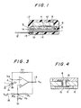
- Figure 1 is a cross-sectional view of one embodiment of a temperature sensor constructed in accordance with the present invention.
- Figure 2 illustrates the steps of manufacturing the temperature sensor shown in Figure 1.
- Figure 3 is a circuit diagram of the CR oscillating circuit.
- Figure 4 is a cross-sectional view passing through a contact section connecting between the first and second conductive patterns.
- Figure 5 is a time chart illustrating the operation of the temperature shown in Figure 1.
- Figure 6 is a graph illustrating the output characteristics of the temperature sensor shown in Figure 1.
- Figure 7 is a graph illustrating the relationship between the temperature and the specific dielectric constant in the ceramic dielectric body.
- Referring now to Figures 1 and 2, there is shown a ceramic dielectric body 1 which is ground into 0.5 mm thickness by any suitable grinding manner such as lapping and severed into a rectangular plate having its dimensions of 5
mm X 8 mm, as shown in Figure 2 (a). The ceramic dielectric body 1 serves as a dielectric for acapacitor 2 in a CR oscillating circuit shown in Figure 3. The term "CR oscillating circuit" in the present invention is referred to as an oscillating circuit which includes a positive feedback consisting of capacitances and resistances. - The ceramic dielectric plate 1 also is used as a circuit substrate. On one side 1a of the ceramic dielectric plate 1 are printed and baked a first resistor 3 (resistor Rf in Figure 3), one of the
electrodes 5 in thecapacitor 2 and a first electricallyconductive pattern 5 connecting thefirst resistor 3 with thecapacitor 2, all of which are parts of the CR oscillating circuit, as shown in Figure 2 (b). For example, theelectrode 4 is of a size of about 2 mm X about 2 mm. In the present embodiment, some of resistors R₁, R₂, R₃ and Rf defining the CR oscillating circuit, for example, resistors R₁, R₂ and R₃ are formed directly on the surface of the ceramic dielectric plate 1 from the resistor paste by means of the printing and backing technique. Theelectrode 4 is formed by screen printing an electrode pattern from a material consisting of silver and palladium on the surface of the ceramic dielectric plate 1 and then baking the electrode pattern at a temperature equal to about 850 °C. - All the
first resistor 3,electrode 4 and first electricallyconductive pattern 5 formed on the ceramic dielectric plate 1 are covered with an electrically insulatinglayer 6, as seen from Figure 2 (c). Theinsulation layer 6 is formed by printing an electrically insulating material on theaforementioned resistor 3 and other components and baking it after dried. In the present embodiment, a plurality of suchinsulating layers 6 are formed one above another repeatedly (for example, two or three times) into a relatively thickened lamination so that the insulation failure can be positively prevented. Further, theinsulating layer 6 is pre-formed with openings at positions corresponding to through holes which are used to connect some parts on one side of the substrate 1 with the respective parts on the other side of the same. - On the opposite or exterior surface of the
insulating layer 6 are formed the other resistors of the CR oscillating circuit, that is, second resistors 7 (R₁, R₂ and R₃) and a second electricallyconductive pattern 8 connected with the second resistors 7 in the same manner. On the secondconductive pattern 8 is soldered amini-flat package 10 of IC as an active component, as seen from Figure 2 (e). Themini-flat package 10 includes an operational amplifier 11 integratedly formed therein. - On the opposite face 1b of the ceramic dielectric plate 1 is similarly printed and baked an electrically
conductive pattern portion 13 for attachinglead 12 thereto and theother electrode 14 of thecapacitor 2, as seen from Figure 2 (f). In the present embodiment, saidother electrode 14 is formed substantially over the overall surface of the face 1b of the ceramic dielectric plate 1 and also grounded to provide a ground electrode (GND electrode). As seen from Figure 3, the substrate 1 also includes electrodes to be connected with aVcc input terminal 18 and aVo output terminal 19, respectively. - As shown in Figure 4, the
insulating layer 6 is formed with a throughhole 15 in which an electricallyconductive contact portion 16 is formed in the form of a via-hole electrode. The firstconductive pattern 5 is electrically connected with the secondconductive pattern 8 through the via-hole electrode 16. In Figure 4, the ceramic dielectric body 1,mini-flat package 10 and others are omitted. The firstconductive pattern 5 also is electrically connected with theconductive pattern portion 13 through a through-hole electrode (not shown). Thus, the CR oscillating circuit will be formed on the ceramic dielectric plate 1 in the form of an integral lamination. The overall surface of the CR oscillating circuit is covered and protected with a dip paint layer (dip package) 17 of an electrically insulating plastic resin, as seen from Figure 2 (f). - The part of the ceramic dielectric plate 1 located between the
electrodes capacitor 2. In order to cause the role of this dielectric portion to perform efficiently, the ceramic dielectric body 1 is so selected that it has a working temperature range for temperature detection in the normal dielectric phase and a temperature coefficient for dielectric constant which is ranged between -1,000 ppm and -10,000 ppm. One of such ceramic materials is (SrPb)TiO₃-Bi₃ 2TiO₂. - In general, the ceramic dielectric has such a relationship between the specific dielectric constant εr and the temperature T as shown in Figure 7. If it is desired to apply the dielectric to a capacitor for sensing temperature, it is required to use substantially lineaer parts of the curve shown in Figure 7, that is, a linear portion A corresponding to the temperature range lower than the Curie temperatur Tc (and substantially proportional to the temperature T) and another linear portion B corresponding to the temperature range higher than the Curie temperature Tc (and substantially proportional to 1/T). However, the linear portion A is less stable in the temperature-specific dielectric constant characteristics and therefore not preferable for the dielectric in the temperature sensor. On the contrary, the linear portion B is more stable in the temperature-specific dielectric constant characteristics and preferable for the dielectric in the temperature sensor.
- From the viewpoint of the sensitivity in the temperature detection, it is further preferable that the gradient in the linear portion B shown in Figure 7, that is, temperature coefficient, is high as far as possible. On the other hand, there is also known dielectric materials having their working temperature ranges in the heavy dielectric phase. However, such dielectric materials are not preferable in that they are less stable in the relationship between the specific dielectric constant εr and the temperature. In view of this, the present invention utilizes a capcitor incorporating a ceramic dielectric body which has a temperature coefficient ranged between -1,000 ppm and -10,000 ppm and a working temperature range in the normal dielectric phase.
- The above range of the temperature coefficient in the present invention is selected for the following reasons:
- (a) If the temperature coefficient is larger than -1,000 ppm, the sensitivity of the temperature sensor decreases as the temperature coefficient approaches zero. It may be impossible to perform any practical detection of temperature.
- (b) If the absolute value of the temperature coefficient is laerger than -10,000 ppm, the rate of variation increases up to unacceptable degrees for ceramic materials which have been developed up-to-dately.
- Although the dielectric materials having their working temperature range in the normal dielectric phase includes organic materials such as plastics, the plastics cannot be printed and baked as electrically conductive patterns on the substrate since they may be fused at high baking temperatures. It is of course that the CR oscillating circuit may be two-dimensionally formed on the substrate in any suitable manner other than the printing and baking technique. However, this raises another problem in that the substrate should be increased in size, resulting in increase of the overal size of the temperature sensor. In accordance with the present invention, the temperature sensor can be provided by printing and baking the dielectric material on the substrate. As a result, the temperature the sensor can be extemely easily manufactured in the form of a three-dimensional and integral lamination which results in decrease of the overal size of the temperature sensor.
- In the present embodiment, the frequency of the CR oscillating circuit can be adjusted by changing the electrostatic capacity of the
capacitor 2. Concretely, the electrostatic capacity of thecapacitor 2 can be changed by trimming the groundedelectrode 14 thereof to regulate the area of electrode. Other method of regulating the oscillating frequency includes the regulation of the level of resistance in the resistor Rf or the combined resistors R₁, R₂ and R₃, as shown in Figure 3. - Although the ceramic dielectric bulk is used to provide the substrate on which the CR oscillating circuit is formed in the present embodiment, the ceramic dielectric bulk may be replaced by a ceramic dielectric substrate which is integrally formed by providing a green sheet of ceramic dielectric, and printing and baking a plurality of layers from electrode and resistor pastes on the sheet. In such a case, the green sheet is prepared by grinding a ceramic dielectric material after calcination, adding an organic binder, water and an organic solvent into the ground material to form a mixture, pot powdering the mixture to form a slurry and sheeting the slurry by the use of the doctor blade process. Electrodes and resistors are screen printed in place on the substrate. The electrical connection between the layers on the sheet is accomplished through via-holes which are formed by the through-hole process. The frequency of the CR oscillating section can be more easily adjusted by forming and regulating a resistor Rf on the substrate. Usually, the thickness of the green sheet may be equal to about 0.7 mm.
- The temperature sensor constructed in the above manner will be further described with respect to its operation in connection with the CR oscillating circuit of Figure 3 and a time chart of Figure 5.
- First of all, a reference voltage is applied to the
input terminal 18 of the CR oscillating circuit. This voltage signal is then supplied to the plus terminal of the operational amplifier 11 through the resistor R₃. At this time, the voltage VA applied to the plus terminal is represented as square waves oscillating between the maximum voltage Vz and the minimum voltage V₁ as show in Figure 5 (a). On application of the reference voltage, an electric current will flow in theelectrode 4 of thecapacitor 2 through the resistor Rf to charge thecapacitor 2. On progress of the charge, the voltage on theelectrode 4, that is, the voltage VB on the minus terminal of the operational amplifier 11 gradually increases from a point X to another point Y for a period of time between T₁ and T₂, as seen from Figure 5 (b). Thus, the operational amplifier 11 serves as a comparator which compares the voltage VA with the voltage VB. If the voltage VA is higher than the voltage VB, an output signal of voltage V₂₀ will be generated from theoutput terminal 19, as shown in Figure 5 (c). If VA=VB=V₂ at time T₂, the output signal of the operational amplifier 11 is inverted to generated an output signal of voltage V₁₀ between T₂ and T₃. At the time T₂, therefore, thecapacitor 2 initiates its discharge from the point Y to a point Z. IF VA=VB=V₁ at time T₃, the output signal of the operational amplifier 11 is again inverted to generate an output signal of voltage V₂₀. Thus, thecapcitor 2 is re-charged for a period of time between T₃ and T₄. By repeating a cycle consisting of the charge and discharge of thecapcitor 2 and the signal inversion of the operational amplifier 11, square wave signal V₀ will be outputted from the CR oscillating circuit. - Since the specific dielectric constant εr of the ceramic dielectric body 1 varies depending on the variations of ambient temperature, the electrostatic capacity of the
capacitor 2 also varies correspondingly. In other words, the electrostatic capacity of the capacitor decreases as the ambient temperature increases. Therefore, the time intervals on the charge and discharge correspondingly decrease to increase the frequency of the output signal fromthe output terminal of the CR oscillating circuit. On the contrary, as the ambient temperature decreases, the electrostatic capacity of the capacitor increases to decrease the frequency of the output signal from the output terminal of the CR oscillating circuit. - Thus, the present temperature can be determined by analyzing the frequency of the output signal from the CR oscillating circuit.
- Figure 6 illustrates the output characteristics of the temperature sensor constructed in accordance with the aforementioned embodiment of the present invention. The output characteristics were measured with respect to the temperature sensor which utilized a ceramic dielectric having its temperature coefficient equal to -4,700 ppm.
- As seen from Figure 6, the temperature T is substantially proportional to the output frequency f through a temperature range between -20 °C and 120 °C. This means that the temperature sensor according to the present invention can sufficiently meet the accuracy of detection required in various electric home appliances.
- Since the present invention the CR oscillating circuit formed on the ceramic dielectric substrate 1 and the insulating
layer 6 covering the surface of the same, the substrate itself can be reduced in size to decrease the overall size of temperature sensor. - Since the CR oscillating circuit of the present invention is integrally formed by printing and baking the resistors and the conductive patterns on the ceramic dielectric substrate 1, it is not necessary to conect between various parts in the circuit through leads. This means that less noises penetrate into the circuit to provide a very reliable detection of temperature. Further, since one of the
electrodes 14 of thecapacitor 2 is formed on the ceramic dielectric substrate 1 over its more area and yet connected with the ground, noises from the interior and exterior of the circuit can be caught by the grounded electrode. Therefore, S/N ratio in the oscillating circuit can be extremely improved to further increase the reliablity on the temperature detection. - Although the present invention has been described as to the comparison of the reference voltage VA with the electrode voltage VB at the operational amplifier 11, the present invention is not limited to such an arrangement. For example, a separate comparator may be used to compare the voltage VA with the voltage VB.
- Although the present invention has been described as to the arrangement in which the
electrodes capacitor 2 are provided on the opposite sides of the ceramic dielectric substrate 1, one of theelectrodes other electrode - Although the present invention has been described as to the temperature sensor including the circuit protecting dip-paint layer of plastic material, it may be replaced by the formation of a passivation film from aluminum nitride or silicon oxide by any suitable means such as CVD and the like. In the latter case, it is anticipated that the thermal capacity of the sensor can be reduced to improve the responsibility thereof relative to the variations of temperature.
- As be apparent from the foregoing, the present invention can decrease the number of parts to be used and simplify the overall construction of the circuit. Further, since the ceramic dielectric body is superior in thermal resistance, the resistors and conductive patterns in the CR oscillating circuit can be integrally printed and baked, such that the circuit may more efficiently be manufactured with decrease of the size of the temperature sensor.
- Since the temperature sensor of the present invention is so constructed that the frequency of the output signal can be varied depending on the variations of ambient temperature, the output frequency can be immediately counted by any counting circuit in a micro-computer if the output signals from the temperature sensor are inputted directly into the micro-computer. The resulting counts can be used to perform the instant determination of temperatures detected. Thus, the process of handling signals in the micro-computer can be promoted extremely. Furthermore, the present invention does not require and A/D converter which was absolutely required in the prior art. It is thus intended to simplify the construction of the apparatus and to reduce the manufacturing cost thereof.
- Since the ceramic dielectric body used in the temperature sensor of the present invention has its working temperature range in the normal dielectric phase, it has its very stable variation in the specific dielectric constant relative to the variations of temperature. In addition, the sensitivity on temperature detection also is superior with an increased reliability of temperature detection since the temperature coefficient of the dielectric constant in the ceramic dielectric body is ranged between -1,000 ppm and -10,000 ppm.
Claims (6)
Applications Claiming Priority (2)
| Application Number | Priority Date | Filing Date | Title |
|---|---|---|---|
| JP245270/87 | 1987-09-29 | ||
| JP62245270A JPS6488128A (en) | 1987-09-29 | 1987-09-29 | Temperature sensor |
Publications (3)
| Publication Number | Publication Date |
|---|---|
| EP0310101A2 true EP0310101A2 (en) | 1989-04-05 |
| EP0310101A3 EP0310101A3 (en) | 1990-02-14 |
| EP0310101B1 EP0310101B1 (en) | 1992-12-09 |
Family
ID=17131182
Family Applications (1)
| Application Number | Title | Priority Date | Filing Date |
|---|---|---|---|
| EP88116147A Expired - Lifetime EP0310101B1 (en) | 1987-09-29 | 1988-09-29 | Temperature sensor |
Country Status (4)
| Country | Link |
|---|---|
| US (1) | US4883366A (en) |
| EP (1) | EP0310101B1 (en) |
| JP (1) | JPS6488128A (en) |
| DE (1) | DE3876579T2 (en) |
Cited By (4)
| Publication number | Priority date | Publication date | Assignee | Title |
|---|---|---|---|---|
| EP0713065A1 (en) * | 1994-11-17 | 1996-05-22 | Whirlpool Europe B.V. | Compact-dimension device for sensing frost on a refrigerator evaporator |
| US6534767B1 (en) | 1996-11-06 | 2003-03-18 | European Atomic Energy Community (Euratom) | Temperature sensor and sensing apparatus |
| WO2008110949A1 (en) * | 2007-03-15 | 2008-09-18 | Koninklijke Philips Electronics N.V. | Methods and devices for measuring core body temperature |
| RU2497441C2 (en) * | 2008-07-28 | 2013-11-10 | Омрон Хэлткэа Ко., Лтд. | Electronic thermometer |
Families Citing this family (14)
| Publication number | Priority date | Publication date | Assignee | Title |
|---|---|---|---|---|
| DE4035952C1 (en) * | 1990-11-09 | 1992-06-17 | Abb Patent Gmbh, 6800 Mannheim, De | Method of measuring temperature of electrical conductors - has electrode forming condenser with capacitance compared to calibration graph |
| GB9217436D0 (en) * | 1992-08-17 | 1992-09-30 | De Beers Ind Diamond | Diamond temperature sensor |
| US6337389B1 (en) * | 1995-03-17 | 2002-01-08 | Bioscience Consultants, L.L.C. | Method and process for the production of collagen preparations from invertebrate marine animals and compositions thereof |
| JP4121707B2 (en) * | 1998-09-02 | 2008-07-23 | 株式会社前川製作所 | Non-contact food temperature measuring device for food |
| US6568849B1 (en) * | 2000-04-07 | 2003-05-27 | Cyntec Company | Temperature probe with improved structure integrity and operation reliability over high temperature and voltage |
| WO2004074794A1 (en) * | 2003-02-20 | 2004-09-02 | Ysi Incorporated | Digitally modified resistive output for a temperature sensor |
| JP4603299B2 (en) * | 2004-06-11 | 2010-12-22 | ホーチキ株式会社 | Heat sensor |
| JP4741849B2 (en) * | 2005-02-07 | 2011-08-10 | ホーチキ株式会社 | Method for manufacturing thermal sensing element |
| US7810993B2 (en) * | 2007-02-06 | 2010-10-12 | Chevron U.S.A. Inc. | Temperature sensor having a rotational response to the environment |
| KR200456132Y1 (en) * | 2009-01-13 | 2011-10-13 | (주) 래트론 | Sensor element protected by film layer and resin layer |
| FR2985309B1 (en) * | 2012-01-02 | 2014-01-24 | Commissariat Energie Atomique | CAPACITIVE TEMPERATURE SENSOR COMPRISING TWO CAPACITORS ON A VOLTAGE DIVIDER BRIDGE |
| EP3150105B1 (en) * | 2013-03-19 | 2018-09-05 | Olympus Corporation | Endoscope apparatus |
| RU2543695C1 (en) * | 2013-08-01 | 2015-03-10 | Ренат Ильгизович Шайдуллин | Method to measure temperature of polymer coating of fibre light guide |
| US11117478B2 (en) * | 2018-09-24 | 2021-09-14 | Te Connectivity Corporation | Charging inlet with thermal sensor |
Citations (4)
| Publication number | Priority date | Publication date | Assignee | Title |
|---|---|---|---|---|
| GB998534A (en) * | 1961-03-27 | 1965-07-14 | Intron Int Inc | Thermally sensitive capacitive circuit element |
| US3814999A (en) * | 1973-05-15 | 1974-06-04 | Corning Glass Works | Cryogenic capacitive bolometer |
| US3869398A (en) * | 1972-09-20 | 1975-03-04 | Taiyo Yuden Kk | Dielectric porcelain composition |
| US4545254A (en) * | 1984-06-01 | 1985-10-08 | Ceramphysics, Inc. | Materials and methods for pressure and temperature sensors at cryogenic temperatures |
Family Cites Families (12)
| Publication number | Priority date | Publication date | Assignee | Title |
|---|---|---|---|---|
| US2659801A (en) * | 1950-10-06 | 1953-11-17 | Gen Electric | Temperature control device |
| US3260116A (en) * | 1963-05-15 | 1966-07-12 | Gen Electric | Remote reading temperature indicating system |
| US3851320A (en) * | 1973-11-08 | 1974-11-26 | Bio Data Inc | External temperature and pulse rate sensing and transmitting device |
| JPS5220259A (en) * | 1975-08-08 | 1977-02-16 | Taiyo Yuden Kk | Cylinderical throughhtype ceramic condenser and its fabrication method |
| US4213797A (en) * | 1978-03-23 | 1980-07-22 | Arden Sher | Radiant energy to electric energy converter |
| US4267634A (en) * | 1978-04-05 | 1981-05-19 | American Components Inc. | Method for making a chip circuit component |
| US4247881A (en) * | 1979-04-02 | 1981-01-27 | Sprague Electric Company | Discoidal monolithic ceramic capacitor |
| EP0111890B1 (en) * | 1982-12-15 | 1991-03-13 | Nec Corporation | Monolithic multicomponents ceramic substrate with at least one dielectric layer of a composition having a perovskite structure |
| JPS60249386A (en) * | 1984-05-24 | 1985-12-10 | キヤノン株式会社 | Functional substrate and electronic circuit substrate using same |
| JPS61250905A (en) * | 1985-04-26 | 1986-11-08 | ティーディーケイ株式会社 | Dielectric ceramic composition and manufacture thereof |
| JPS62157607A (en) * | 1985-12-30 | 1987-07-13 | 太陽誘電株式会社 | Dielectric porcelain compound |
| JPS62194607A (en) * | 1986-02-20 | 1987-08-27 | 株式会社村田製作所 | Ceramic capacitor |
-
1987
- 1987-09-29 JP JP62245270A patent/JPS6488128A/en active Granted
-
1988
- 1988-09-28 US US07/250,738 patent/US4883366A/en not_active Expired - Lifetime
- 1988-09-29 DE DE8888116147T patent/DE3876579T2/en not_active Expired - Fee Related
- 1988-09-29 EP EP88116147A patent/EP0310101B1/en not_active Expired - Lifetime
Patent Citations (4)
| Publication number | Priority date | Publication date | Assignee | Title |
|---|---|---|---|---|
| GB998534A (en) * | 1961-03-27 | 1965-07-14 | Intron Int Inc | Thermally sensitive capacitive circuit element |
| US3869398A (en) * | 1972-09-20 | 1975-03-04 | Taiyo Yuden Kk | Dielectric porcelain composition |
| US3814999A (en) * | 1973-05-15 | 1974-06-04 | Corning Glass Works | Cryogenic capacitive bolometer |
| US4545254A (en) * | 1984-06-01 | 1985-10-08 | Ceramphysics, Inc. | Materials and methods for pressure and temperature sensors at cryogenic temperatures |
Non-Patent Citations (2)
| Title |
|---|
| IEEE TRANSACTIONS ON ELECTRON DEVICES, vol. ED-29, no. 1, January 1982, pages 95-101, IEEE, New York, US; T. NITTA et al.: "Multifunctional ceramic sensors: Humidity-gas sensor and temperature-humidity sensor" * |
| THE REVIEW OF SCIENTIFIC INSTRUMENTS, vol. 37, no. 4, April 1966, pages 495-496; S.J. FABRICANT et al.: "Ultracentrifuge rotor temperature measurements and control" * |
Cited By (5)
| Publication number | Priority date | Publication date | Assignee | Title |
|---|---|---|---|---|
| EP0713065A1 (en) * | 1994-11-17 | 1996-05-22 | Whirlpool Europe B.V. | Compact-dimension device for sensing frost on a refrigerator evaporator |
| US6534767B1 (en) | 1996-11-06 | 2003-03-18 | European Atomic Energy Community (Euratom) | Temperature sensor and sensing apparatus |
| WO2008110949A1 (en) * | 2007-03-15 | 2008-09-18 | Koninklijke Philips Electronics N.V. | Methods and devices for measuring core body temperature |
| US9410854B2 (en) | 2007-03-15 | 2016-08-09 | Koninklijke Philips N.V. | Methods and devices for measuring core body temperature |
| RU2497441C2 (en) * | 2008-07-28 | 2013-11-10 | Омрон Хэлткэа Ко., Лтд. | Electronic thermometer |
Also Published As
| Publication number | Publication date |
|---|---|
| US4883366A (en) | 1989-11-28 |
| JPS6488128A (en) | 1989-04-03 |
| EP0310101A3 (en) | 1990-02-14 |
| JPH0567167B2 (en) | 1993-09-24 |
| DE3876579D1 (en) | 1993-01-21 |
| DE3876579T2 (en) | 1993-07-01 |
| EP0310101B1 (en) | 1992-12-09 |
Similar Documents
| Publication | Publication Date | Title |
|---|---|---|
| US4883366A (en) | Temperature sensor | |
| EP0033520B1 (en) | Multi-functional sensing or measuring system | |
| US5410291A (en) | Thermistor type temperature sensor | |
| US5130600A (en) | Acceleration sensor | |
| US4262532A (en) | Pressure and temperature sensor | |
| US5041809A (en) | Glass-ceramic temperature sensor for heating ovens | |
| EP2257824A1 (en) | Method and system for adjusting characteristics of integrated relative humidity sensor | |
| EP0751383A1 (en) | Sensor with output correcting function | |
| GB2222261A (en) | Humidity measuring apparatus | |
| US4793175A (en) | Humidity sensor, sensor material, method of manufacture and humidity sensing system, especially for automotive use | |
| US6147481A (en) | Termination for RF circuit which senses changes in power and which is not temperature sensitive | |
| US5040417A (en) | Electronic relative humidity/temperature measuring system | |
| US6456096B1 (en) | Monolithically compatible impedance measurement | |
| US4789822A (en) | Three-electrode sensor for phase comparison and pulse phase adjusting circuit for use with the sensor | |
| US6407631B2 (en) | Charge-type sensor amplifying circuit | |
| EP0257724A2 (en) | Three-electrode sensor for phase comparison and pulse phase adjusting circuit for use with the sensor | |
| JPH03172719A (en) | Level sensor | |
| JPS56164949A (en) | Multifunction detector | |
| JP3106385B2 (en) | High frequency detecting element and high frequency heating device using the same | |
| US4164147A (en) | Temperature sensing apparatus | |
| KR100504783B1 (en) | Module of humidity sensor equipped with heater and humidity sensing method thereof | |
| JPS6152945B2 (en) | ||
| JP3365013B2 (en) | Thermistor with built-in pull-up resistor | |
| JP3419409B2 (en) | Strain detector | |
| JPH0548106Y2 (en) |
Legal Events
| Date | Code | Title | Description |
|---|---|---|---|
| PUAI | Public reference made under article 153(3) epc to a published international application that has entered the european phase |
Free format text: ORIGINAL CODE: 0009012 |
|
| AK | Designated contracting states |
Kind code of ref document: A2 Designated state(s): DE FR GB |
|
| PUAL | Search report despatched |
Free format text: ORIGINAL CODE: 0009013 |
|
| AK | Designated contracting states |
Kind code of ref document: A3 Designated state(s): DE FR GB |
|
| 17P | Request for examination filed |
Effective date: 19900309 |
|
| 17Q | First examination report despatched |
Effective date: 19910717 |
|
| GRAA | (expected) grant |
Free format text: ORIGINAL CODE: 0009210 |
|
| AK | Designated contracting states |
Kind code of ref document: B1 Designated state(s): DE FR GB |
|
| REF | Corresponds to: |
Ref document number: 3876579 Country of ref document: DE Date of ref document: 19930121 |
|
| ET | Fr: translation filed | ||
| PLBE | No opposition filed within time limit |
Free format text: ORIGINAL CODE: 0009261 |
|
| STAA | Information on the status of an ep patent application or granted ep patent |
Free format text: STATUS: NO OPPOSITION FILED WITHIN TIME LIMIT |
|
| 26N | No opposition filed | ||
| REG | Reference to a national code |
Ref country code: GB Ref legal event code: IF02 |
|
| PGFP | Annual fee paid to national office [announced via postgrant information from national office to epo] |
Ref country code: FR Payment date: 20040908 Year of fee payment: 17 |
|
| PGFP | Annual fee paid to national office [announced via postgrant information from national office to epo] |
Ref country code: DE Payment date: 20040923 Year of fee payment: 17 |
|
| PGFP | Annual fee paid to national office [announced via postgrant information from national office to epo] |
Ref country code: GB Payment date: 20040929 Year of fee payment: 17 |
|
| PG25 | Lapsed in a contracting state [announced via postgrant information from national office to epo] |
Ref country code: GB Free format text: LAPSE BECAUSE OF NON-PAYMENT OF DUE FEES Effective date: 20050929 |
|
| PG25 | Lapsed in a contracting state [announced via postgrant information from national office to epo] |
Ref country code: DE Free format text: LAPSE BECAUSE OF NON-PAYMENT OF DUE FEES Effective date: 20060401 |
|
| GBPC | Gb: european patent ceased through non-payment of renewal fee |
Effective date: 20050929 |
|
| PG25 | Lapsed in a contracting state [announced via postgrant information from national office to epo] |
Ref country code: FR Free format text: LAPSE BECAUSE OF NON-PAYMENT OF DUE FEES Effective date: 20060531 |
|
| REG | Reference to a national code |
Ref country code: FR Ref legal event code: ST Effective date: 20060531 |