EP0310069B1 - Method of generating discretization grid for finite-difference simulation - Google Patents
Method of generating discretization grid for finite-difference simulation Download PDFInfo
- Publication number
- EP0310069B1 EP0310069B1 EP88116071A EP88116071A EP0310069B1 EP 0310069 B1 EP0310069 B1 EP 0310069B1 EP 88116071 A EP88116071 A EP 88116071A EP 88116071 A EP88116071 A EP 88116071A EP 0310069 B1 EP0310069 B1 EP 0310069B1
- Authority
- EP
- European Patent Office
- Prior art keywords
- grid
- rectangular grid
- generating
- rectangular
- intersection
- Prior art date
- Legal status (The legal status is an assumption and is not a legal conclusion. Google has not performed a legal analysis and makes no representation as to the accuracy of the status listed.)
- Expired - Lifetime
Links
Images



Classifications
-
- G—PHYSICS
- G06—COMPUTING OR CALCULATING; COUNTING
- G06F—ELECTRIC DIGITAL DATA PROCESSING
- G06F30/00—Computer-aided design [CAD]
- G06F30/20—Design optimisation, verification or simulation
- G06F30/23—Design optimisation, verification or simulation using finite element methods [FEM] or finite difference methods [FDM]
Definitions
- the present invention relates to a numerical simulation technique known as a finite-difference simulation and, more particularly, to a method of generating a discretization grid necessary for finite-difference simulation.
- a numerical simulation technique known as finite-difference simulation is particularly useful in analyzing Voltage-Current characteristic and response characteristic of semi-conductor devices (See, for example, S. Selberherr "Analysis and Simulation of Semiconductor Devices” Springer-Verlag, Wien, 1984).
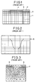
- a discretization grid is superimposed on the cross-sectional figure of a semi-conductor device to be simulated, as shown in Fig. 1.
- grid points separations between adjacent intersections of a vertical line and a horizontal line (referred hereafter simply as grid points) are reduced near boundaries of different materials such as a boundary 3 between semi-conductor base 1 and insulator medium 2, or peripheral region 5 of the electrode medium 4.
- the discretization grid is generated such that grid points lie on these boundaries.
- the physical quantities such as potentials, electron densities etc. are calculated on these grid points, and prediction or evaluation of the Voltage-Current characteristic, the response characteristic etc. are derived from these simulated quantities.
- the discretization grid used for finite-difference simulation most commonly is a rectangular grid such as the one shown in Fig. 1.
- This object is achieved in the present invention by providing a method of generating a discretization grid for a finite-difference simulation as set out in claim 1.
- Fig. 1 is an illustration of a rectangular grid of a first prior art method.
- Fig. 2 is an illustration of a rectangular grid to simulate a complicated polygonal figure in the first prior art method.
- Fig. 3 is an illustration of a triangular grid of a second prior art method.
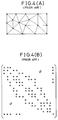
- Fig. 4(A) and (B) are illustrations showing a particular configuration of a triangular grid and a matrix involved in calculations required for this configuration, respectively, in the second prior art method.
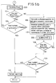
- Fig. 5 is a main flow chart of a method for generating a discretization grid according to the present invention.
- Fig. 6 is a flow chart of a subroutine to be used in the method shown in Fig. 5.
- Fig. 7(a), (b), (c) and (d) are illustrations of discretization grids generated at different stages of the method for generating the discretization grid according to the present invention.
- Fig. 8 is an illustration showing a matrix involved in calculations required by the method according to the present invention.
- the method is executed by an ordinary computer equipped with CPU, ROM, RAM, input device, output device, etc. All calculations and other operations needed at each step of the method are carried out by CPU and all the memorizations of the information needed in the method are handled by RAM or other memory devices.
- Fig. 5 there is shown a main flow-chart of this embodiment of the present invention.
- step 100 input data on a polygonal figure representing the inner structures of a semi-conductor device to be simulated are entered and their units are converted into those appropriate for the computer.
- step 101 material data contained in the input data indicating material of each section of the polygonal figure, such as a semi-conductor on an insulator, are read out and stored in the memory.
- straight lines parallel to the orthogonal coordinate axes (referred hereafter simply as grid lines) are drawn through each vertex of the polygonal figure.
- step 102 ensures that there is a grid point on each vertex of the polygonal figure.
- step 103 boundaries between different materials which are parallel to the orthogonal coordinate axes are identified from the material data obtained at the step 101, and additional grid points and grid lines through them are generated near the identified boundaries so as to reduce the separations between grid lines in this region.
- coordinates of the newly generated grid points are determined, and from all coordinates overlaps are removed while the remaining coordinates are arranged in order and stored in the memory.
- This step 103 ensures that the grid is finer around boundaries of different materials.
- the coordinates stored in the memory at this point are then given to the subroutine 200 shown in Fig. 6.
- the total number of grid points are compared with a prescribed threshold value. If the total number is greater than the threshold value, the step 206, which will be explained later, will be taken. Otherwise, the step 202 will be taken, where segments of the polygonal figure which are not parallel to the orthogonal coordinate axes (referred hereafter simply as oblique segments) are identified, and further additional grid points and grid lines through them are generated at intersections of one of the grid lines and the identified oblique segments. Then coordinates of the newly generated grid points are determined, marked as new in order to distinguish from those existed before entering this step, and stored in the memory.
- step 203 whether all the grid lines have been checked at the step 202 is determined. If so, the step 204 will be taken. Otherwise, the step 202 is repeated for the next unchecked grid line.
- step 204 from all the coordinates overlaps are removed and the remaining coordinates are arranged in order and stored in the memory.
- step 205 the step 201 is repeated except here if the total number is greater than the threshold value, the step 206 will be taken while otherwise the step 207, which will be explained later, will be taken.
- step 206 an arbitrary grid line from those newly generated in the subroutine 200 is deleted, and then the step 205 will be repeated. This loop formed by the steps 205 and 206 is intended to remove excessive grid lines.
- step 207 further additional grid points and grid lines through them are generated such that each distance between adjacent grid points has a ratio less than a prescribed ratio to the adjacent distance.
- This can be done, for example, by repeatedly taking an arithmetic mean of the adjacent coordinates and generating new grid points and grid lines through them at that point until the requirement is satisfied.
- the coordinates of the newly generated grid points are determined, and from all the coordinates overlaps are removed and the remaining coordinates are arranged in order and stored in the memory.
- the subroutine 200 ends at this point. It can be seen that this subroutine 200 ensures by repeated applications of the step 202 that there is a grid point at each intersection of the grid lines and the oblique segments.
- the subroutine 200 also ensures by the step 207 that the grid becomes coarser or finer gradually. It is worthwhile to mention here that the process of the step 202 may repeat indefinitely when the polygonal figure consists only of oblique segments, in which a new grid line generated at an intersection of one of the grid lines and one of the oblique segments intersects with some other oblique segment and thereby requiring a new grid lines to be generated there, and so on ad infinitum. However, in this embodiment, since any two points are considered overlapping when their separation is less than a prescribed distance as mentioned above, the process of the step 202 will terminate in a finite number of repetition.
- the step 104 will be taken next.
- the step 104 whether any new grid point had been generated at the subroutine 200 is determined. If so, the step 105 will be taken while otherwise the step 106, which will be explained later, will be taken.
- the total number of the grid points are compared with the prescribed threshold value used at the step 200. If the total number is less than the threshold value, the subroutine 200 and the step 104 will be repeated so as to generate enough number of grid lines, while otherwise the step 110, which will be explained later, will be taken.
- a physical quantity such as an impurity distribution is calculated for each pair of adjacent grid points.
- step 107 further additional grid points and grid lines through them are generated in regions where the physical quantity calculated at the step 106 varies radically. Then coordinates of the newly generated grid points are determined, and from all coordinates overlaps are removed while the remaining coordinates are arranged in order and stored in the memory.
- step 108 will be taken, where the step 104 is repeated except here if any new grid line had been generated by the subrountine 200, the subroutine and this step 108 immediately following it will be repeated so as to take care of these new grid lines. Otherwise the step 109 will be taken where the step 105 will be repeated except here if the total number of grid points is less than the threshold value the process terminates, while otherwise the step 110 will be taken.
- the warning indicating that the prescribed threshold value for the total number of grid points has been saturated is delivered and then the process terminates.
- Fig. 7(A) shows the grid after the step 102
- Fig. 7(B) shows the grid after the step 103
- Fig. 7(c) shows the grid after the step 104
- Fig. 7(d) shows the grid after the process terminated. It is clear from Fig. 7 that the grid generated by this embodiment of the present invention is capable of more accurate simulation of the complicated polygonal figure.
- this embodiment is capable of generating the discretization grid which can simulate the complex configuration with improved accuracy.
- the requirements set out as the object of the present invention are all satisfied. Namely, in this embodiment:
Landscapes
- Engineering & Computer Science (AREA)
- Physics & Mathematics (AREA)
- Theoretical Computer Science (AREA)
- Computer Hardware Design (AREA)
- Evolutionary Computation (AREA)
- Geometry (AREA)
- General Engineering & Computer Science (AREA)
- General Physics & Mathematics (AREA)
- Management, Administration, Business Operations System, And Electronic Commerce (AREA)
- Testing Of Individual Semiconductor Devices (AREA)
- Testing Or Measuring Of Semiconductors Or The Like (AREA)
- Complex Calculations (AREA)
Description
- The present invention relates to a numerical simulation technique known as a finite-difference simulation and, more particularly, to a method of generating a discretization grid necessary for finite-difference simulation.
- A numerical simulation technique known as finite-difference simulation is particularly useful in analyzing Voltage-Current characteristic and response characteristic of semi-conductor devices (See, for example, S. Selberherr "Analysis and Simulation of Semiconductor Devices" Springer-Verlag, Wien, 1984).
- In the finite-difference simulation, a discretization grid is superimposed on the cross-sectional figure of a semi-conductor device to be simulated, as shown in Fig. 1. Here, in order to improve accuracy of simulation, separations between adjacent intersections of a vertical line and a horizontal line (referred hereafter simply as grid points) are reduced near boundaries of different materials such as a
boundary 3 betweensemi-conductor base 1 andinsulator medium 2, orperipheral region 5 of the electrode medium 4. The discretization grid is generated such that grid points lie on these boundaries. The physical quantities such as potentials, electron densities etc. are calculated on these grid points, and prediction or evaluation of the Voltage-Current characteristic, the response characteristic etc. are derived from these simulated quantities. The discretization grid used for finite-difference simulation most commonly is a rectangular grid such as the one shown in Fig. 1. - However, as semi-conductor devices become more highly integrated, a cross-sectional figure of the device becomes more complicated such that boundaries between different materials may include segments which are not parallel to the rectangular grid. Though it is possible to simulate such a semi-conductor device with a complex cross-sectional figure by the conventional finite-difference simulation using a rectangular grid, as shown in Fig. 2 where the grid is generated so that there is a grid point over each vertex of the
boundary 6, it is extremely difficult to generate such a grid which satisfies all of the following requirements: - (a) there is a grid point over each vertex of the cross-sectional figure;
- (b) there is a grid point where a line of the rectangular grid crosses a segment of the cross-sectional figure which is not parallel to the grid;
- (c) separations between adjacent grid points vary gradually without a radical change, and the grid is finer around boundaries of different materials;
- (d) the grid can be generated automatically.
- In addition, it is very difficult to generate enough grid points on segments of the figure not parallel to the rectangular grid so as to maintain satisfactory accuracy of the simulation.
- To cope with this situation, a method has been proposed in which the cross-sectional figure of the device is covered by triangles such that each vertex of the cross-sectional figure coincide with a vertex of a triangle, as shown in Fig. 3 (See, for example, S.E. Laux and R.J. Lomax "Numerical Investigation of Mesh Size Convergence Rate of the Finite Element Method in MESFFT Simulation" Solid State Electronics Vol. 24, P485, 1981). In this method, complicated figures like a boundary surface 7 and
electrodes 8 can be simulated. - However, this method has the following problems:
- (a) an obtuse triangle must be avoided in order to maintain the high accuracy of the simulation;
- (b) it is very difficult to generate a triangular grid automatically which has grid points over all verticles of the cross-sectional figure, and which is finer around boundaries of different materials and becomes coarser gradually elsewhere;
- (c) calculations required for the simulation with a triangular grid involve matrices in which non-zero elements appears irregularly. For example, a configuration shown in Fig. 4(A) requires calculations involving a matrix shown in Fig. 4(B) where a non-zero element is represented by star symbols. This requires a computer with a larger memory capacity than that normally required for a simulation with a rectangular grid, and consequently render the method a poor practicality.
- It is therefore an object of the present invention to provide a method of generating a discretization grid for a finite-difference simulation which satisfies the following requirements:
- (a) there is a grid point over each vertex of a cross-sectional figure of an object to be simulated;
- (b) there is a grid point over each intersection of the grid and segments of the cross-sectional figure of the object that are not parallel to the grid;
- (c) the grid becomes coarser or finer gradually;
- (d) the grid is finer around boundaries of different materials;
- (e) the grid is generated automatically.
so that objects with complex structures can be handled with high accuracy without increasing a memory capacity of a computer. - This object is achieved in the present invention by providing a method of generating a discretization grid for a finite-difference simulation as set out in
claim 1. - Other features and advantages of the present invention will become apparent from the following description taken in conjunction with the accompanying drawings.
- Fig. 1 is an illustration of a rectangular grid of a first prior art method.
- Fig. 2 is an illustration of a rectangular grid to simulate a complicated polygonal figure in the first prior art method.
- Fig. 3 is an illustration of a triangular grid of a second prior art method.
- Fig. 4(A) and (B) are illustrations showing a particular configuration of a triangular grid and a matrix involved in calculations required for this configuration, respectively, in the second prior art method.
- Fig. 5 is a main flow chart of a method for generating a discretization grid according to the present invention.
- Fig. 6 is a flow chart of a subroutine to be used in the method shown in Fig. 5.
- Fig. 7(a), (b), (c) and (d) are illustrations of discretization grids generated at different stages of the method for generating the discretization grid according to the present invention.
- Fig. 8 is an illustration showing a matrix involved in calculations required by the method according to the present invention.
- One embodiment of a method of generating a discretization grid for a finite-difference simulation according to the present invention will now be described with references to the Figs. 5, 6, 7, and 8.
- In this embodiment, the method is executed by an ordinary computer equipped with CPU, ROM, RAM, input device, output device, etc. All calculations and other operations needed at each step of the method are carried out by CPU and all the memorizations of the information needed in the method are handled by RAM or other memory devices.
- Referring now to Fig. 5, there is shown a main flow-chart of this embodiment of the present invention. At the
step 100, input data on a polygonal figure representing the inner structures of a semi-conductor device to be simulated are entered and their units are converted into those appropriate for the computer. At the step 101, material data contained in the input data indicating material of each section of the polygonal figure, such as a semi-conductor on an insulator, are read out and stored in the memory. At thestep 102, straight lines parallel to the orthogonal coordinate axes (referred hereafter simply as grid lines) are drawn through each vertex of the polygonal figure. Then coordinates with respect to the orthogonal coordinates of points where vertical and horizontal grid lines intersects (referred hereafter simply as grid points) are determined. After removing overlaps, the remaining coordinates are arranged in order and stored in the memory. In this embodiment, any two points are considered overlapping when their separation is less than a prescribed distance. Thisstep 102 ensures that there is a grid point on each vertex of the polygonal figure. At thestep 103, boundaries between different materials which are parallel to the orthogonal coordinate axes are identified from the material data obtained at the step 101, and additional grid points and grid lines through them are generated near the identified boundaries so as to reduce the separations between grid lines in this region. Then coordinates of the newly generated grid points are determined, and from all coordinates overlaps are removed while the remaining coordinates are arranged in order and stored in the memory. Thisstep 103 ensures that the grid is finer around boundaries of different materials. - The coordinates stored in the memory at this point are then given to the
subroutine 200 shown in Fig. 6. At thestep 201, the total number of grid points are compared with a prescribed threshold value. If the total number is greater than the threshold value, thestep 206, which will be explained later, will be taken. Otherwise, thestep 202 will be taken, where segments of the polygonal figure which are not parallel to the orthogonal coordinate axes (referred hereafter simply as oblique segments) are identified, and further additional grid points and grid lines through them are generated at intersections of one of the grid lines and the identified oblique segments. Then coordinates of the newly generated grid points are determined, marked as new in order to distinguish from those existed before entering this step, and stored in the memory. At thestep 203, whether all the grid lines have been checked at thestep 202 is determined. If so, thestep 204 will be taken. Otherwise, thestep 202 is repeated for the next unchecked grid line. At thestep 204, from all the coordinates overlaps are removed and the remaining coordinates are arranged in order and stored in the memory. Atstep 205, thestep 201 is repeated except here if the total number is greater than the threshold value, thestep 206 will be taken while otherwise thestep 207, which will be explained later, will be taken. At thestep 206, an arbitrary grid line from those newly generated in thesubroutine 200 is deleted, and then thestep 205 will be repeated. This loop formed by thesteps step 207, further additional grid points and grid lines through them are generated such that each distance between adjacent grid points has a ratio less than a prescribed ratio to the adjacent distance. This can be done, for example, by repeatedly taking an arithmetic mean of the adjacent coordinates and generating new grid points and grid lines through them at that point until the requirement is satisfied. Then the coordinates of the newly generated grid points are determined, and from all the coordinates overlaps are removed and the remaining coordinates are arranged in order and stored in the memory. Thesubroutine 200 ends at this point. It can be seen that thissubroutine 200 ensures by repeated applications of thestep 202 that there is a grid point at each intersection of the grid lines and the oblique segments. Thesubroutine 200 also ensures by thestep 207 that the grid becomes coarser or finer gradually. It is worthwhile to mention here that the process of thestep 202 may repeat indefinitely when the polygonal figure consists only of oblique segments, in which a new grid line generated at an intersection of one of the grid lines and one of the oblique segments intersects with some other oblique segment and thereby requiring a new grid lines to be generated there, and so on ad infinitum. However, in this embodiment, since any two points are considered overlapping when their separation is less than a prescribed distance as mentioned above, the process of thestep 202 will terminate in a finite number of repetition. - Returning to the main flow chart of Fig. 5, the
step 104 will be taken next. At thestep 104, whether any new grid point had been generated at thesubroutine 200 is determined. If so, thestep 105 will be taken while otherwise thestep 106, which will be explained later, will be taken. At thestep 105, the total number of the grid points are compared with the prescribed threshold value used at thestep 200. If the total number is less than the threshold value, thesubroutine 200 and thestep 104 will be repeated so as to generate enough number of grid lines, while otherwise thestep 110, which will be explained later, will be taken. At thestep 106, a physical quantity such as an impurity distribution is calculated for each pair of adjacent grid points. At the step 107, further additional grid points and grid lines through them are generated in regions where the physical quantity calculated at thestep 106 varies radically. Then coordinates of the newly generated grid points are determined, and from all coordinates overlaps are removed while the remaining coordinates are arranged in order and stored in the memory. - The coordinates stored in the memory at this point are then given to the
subroutine 200 shown in Fig. 6 again so as to take care of the new grid lines from the step 107, and go through the similar process already explained at the first appearance of thesubroutine 200. After thesubroutine 200, thestep 108 will be taken, where thestep 104 is repeated except here if any new grid line had been generated by thesubrountine 200, the subroutine and thisstep 108 immediately following it will be repeated so as to take care of these new grid lines. Otherwise thestep 109 will be taken where thestep 105 will be repeated except here if the total number of grid points is less than the threshold value the process terminates, while otherwise thestep 110 will be taken. At thestep 110, the warning indicating that the prescribed threshold value for the total number of grid points has been saturated is delivered and then the process terminates. - The discretization grids generated by such steps are shown in Fig. 7, where Fig. 7(A) shows the grid after the
step 102, Fig. 7(B) shows the grid after thestep 103, Fig. 7(c) shows the grid after thestep 104, and Fig. 7(d) shows the grid after the process terminated. It is clear from Fig. 7 that the grid generated by this embodiment of the present invention is capable of more accurate simulation of the complicated polygonal figure. - As has been described, this embodiment is capable of generating the discretization grid which can simulate the complex configuration with improved accuracy. In particular, the requirements set out as the object of the present invention are all satisfied. Namely, in this embodiment:
- (a) there is a grid point over each vertex of a cross-sectional figure of an object to be simulated;
- (b) there is a grid point over each intersection of the grid and segments of the cross-sectional figure of the object that are not parallel to the grid;
- (c) the grid becomes coarser or finer gradually;
- (d) the grid is finer around boundaries of different materials;
- (e) the grid is generated automatically.
- Furthermore, it can be seen from the description of the present invention in comparison with the prior art that since the grid generated by the present invention is parallel to orthogonal coordinate axes, matrices involved in the calculations for the simulation have the form shown in Fig. 8 in which the non-zero elements appears regularly, so that it is not necessary to have a computer with a larger memory capacity in order to perform the method of the present invention.
- Moreover, it can easily be understood that although the preferred embodiment has been described for a simulation of a two dimensional semi-conductor device both for the sake of avoiding possible confusions and being definite, the method can be applied just as advantageously to a three dimensional object and an object of any physical nature so long as it has a definite cross-sectional configuration.
Claims (16)
- A method of automatically generating a rectangular discretization grid for a finite-difference simulation in which particular physical quantities are calculated on grid points of the discretization grid, the method comprising the steps of:(a) generating (102) a rectangular grid to locate one grid point over each vertex of the polygonal figure representing an object to be simulated; the method being further characterized by the steps of(b) generating (202,203) an additional rectangular grid to locate one grid point over each intersection of the rectangular grid generated at the step (a) and segments of the polygonal figure which are not parallel to lines of the rectangular grid; and(c) repeatedly generating (200, 104, 105 ; 200, 108) an additional rectangular grid to locate one grid point over each intersection of the rectangular grid generated at the step (b) and the segments of the polygonal figure which are not parallel to lines of the rectangular grid until every such intersections has one grid point over it.
- The method of claim 1, further comprising the step of:
(d) generating additional rectangular grid near boundaries of different materials so as to make the grid finer in the vicinity of the boundaries. - The method of claim 2, further comprising the step of:
(e) generating an additional rectangular grid to locate one grid point over each intersection of the rectangular grid generated at the step (d) and segments of the polygonal figure which are not parallel to lines of the rectangular grid. - The method of claim 3, further comprising the step of:
(f) repeatedly generating an additional rectangular grid to locate one grid point over each intersection of the rectangular grid and the segments of the polygonal figure which are not parallel to lines of the rectangular grid until every such intersection has one grid point over it. - The method of claim 1, further comprising the step of:
(g) generating additional rectangular grid such that each separation between adjacent lines of the grid has a prescribed ratio to adjacent separation. - The method of claim 5, further comprising the step of:
(h) generating an additional rectangular grid to locate one grid point over each intersection of the rectangular grid generated at the step (g) and segments of the polygonal figure which are not parallel to lines of the rectangular grid. - The method of claim 6, further comprising the step of:
(i) repeatedly generating an additional rectangular grid to locate one grid point over each intersection of the rectangular grid and the segments of the polygonal figure which are not parallel to lines of the rectangular grid until every such intersection has one grid point over it. - The method of claim 1, further comprising the steps of:(j) calculating a physical quantity for each pair of adjacent grid points;(k) generating additional rectangular grid in regions where the physical quantities calculated at the step (j) vary radically so as to make the grid finer in the vicinity of the regions.
- The method of claim 8, further comprising the step of:
(l) generating an additional rectangular grid to locate one grid point over each intersection of the rectangular grid generated at the step (k) and segments of the polygonal figure which are not parallel to lines of the rectangular grid. - The method of claim 9, further comprising the step of:
(m) repeatedly generating an additional rectangular grid to locate one grid point over each intersection of the rectangular grid and the segments of the polygonal figure which are not parallel to lines of the rectangular grid until every such intersection has one grid point over it. - The method of claim 1, further comprising the step of:
(n) representing each grid point by its coordinate with respect to a coordinate system. - The method of claim 11, further comprising of the step of:
(o) removing all overlapping coordinates and arranging the remaining coordinates in order after each step. - The method of claim 2, wherein the boundaries are indicated by material data.
- The method of claim 5, wherein the step (g) is carried out by repeatedly generating an additional grid point at the mid-point of a separation which does not satisfy the requirement until the requirement is satisfied.
- The method of claim 12, wherein at the step (o), two points are considered overlapping when a separation between them is less than a prescribed distance.
- The method of claim 1, wherein the object to be simulated is a semi-conductor device.
Applications Claiming Priority (2)
| Application Number | Priority Date | Filing Date | Title |
|---|---|---|---|
| JP62242585A JP2635617B2 (en) | 1987-09-29 | 1987-09-29 | Method of generating orthogonal lattice points for evaluating semiconductor device characteristics |
| JP242585/87 | 1987-09-29 |
Publications (3)
| Publication Number | Publication Date |
|---|---|
| EP0310069A2 EP0310069A2 (en) | 1989-04-05 |
| EP0310069A3 EP0310069A3 (en) | 1990-06-13 |
| EP0310069B1 true EP0310069B1 (en) | 1994-12-28 |
Family
ID=17091246
Family Applications (1)
| Application Number | Title | Priority Date | Filing Date |
|---|---|---|---|
| EP88116071A Expired - Lifetime EP0310069B1 (en) | 1987-09-29 | 1988-09-29 | Method of generating discretization grid for finite-difference simulation |
Country Status (4)
| Country | Link |
|---|---|
| US (1) | US4969116A (en) |
| EP (1) | EP0310069B1 (en) |
| JP (1) | JP2635617B2 (en) |
| DE (1) | DE3852596T2 (en) |
Families Citing this family (30)
| Publication number | Priority date | Publication date | Assignee | Title |
|---|---|---|---|---|
| US5684723A (en) * | 1987-11-16 | 1997-11-04 | Fujitsu Limited | Device simulation method and device simulator |
| DE3908684C2 (en) * | 1989-03-16 | 1999-07-08 | Gebelein Udo Dipl Ing Fh Dipl | Method for searching a memory associated with a data processing system and device for carrying out such a method |
| JP2851447B2 (en) * | 1991-03-08 | 1999-01-27 | 三菱電機株式会社 | Shape simulation method |
| US5315537A (en) * | 1991-04-08 | 1994-05-24 | Blacker Teddy D | Automated quadrilateral surface discretization method and apparatus usable to generate mesh in a finite element analysis system |
| JPH0520401A (en) * | 1991-07-12 | 1993-01-29 | Sony Corp | Stereophysical quantity calculation device |
| JP3220250B2 (en) * | 1992-01-09 | 2001-10-22 | 株式会社東芝 | Cell automatic placement method |
| JP3001351B2 (en) * | 1993-06-24 | 2000-01-24 | 日本電気株式会社 | Simulation method |
| JPH0786556A (en) * | 1993-09-17 | 1995-03-31 | Nec Corp | Tetrahedron dividing method |
| US5579249A (en) * | 1993-11-01 | 1996-11-26 | Texas Instruments Incorporated | System for modeling an integrated chip package and method of operation |
| US5848260A (en) * | 1993-12-10 | 1998-12-08 | Exa Corporation | Computer system for simulating physical processes |
| US5677846A (en) * | 1993-12-13 | 1997-10-14 | Nec Corporation | Device simulator and mesh generating method thereof |
| US5606517A (en) * | 1994-06-08 | 1997-02-25 | Exa Corporation | Viscosity reduction in physical process simulation |
| IL112313A (en) * | 1995-01-11 | 1999-08-17 | Nova Measuring Instr Ltd | Method and apparatus for determining a location on a surface of an object |
| US5867590A (en) * | 1995-01-11 | 1999-02-02 | Nova Measuring Instruments, Ltd. | Method and apparatus for determining a location on a surface of an object |
| US5640335A (en) * | 1995-03-23 | 1997-06-17 | Exa Corporation | Collision operators in physical process simulation |
| JP3428232B2 (en) * | 1995-06-16 | 2003-07-22 | 富士通株式会社 | Electromagnetic field strength calculator |
| WO1997020276A1 (en) * | 1995-12-01 | 1997-06-05 | Sonnet Software, Inc. | Conformal meshing for electromagnetic analysis of planar circuits |
| JP2858559B2 (en) * | 1996-04-25 | 1999-02-17 | 日本電気株式会社 | Device simulation method |
| US5896303A (en) * | 1996-10-11 | 1999-04-20 | International Business Machines Corporation | Discretization technique for multi-dimensional semiconductor device simulation |
| US5910902A (en) * | 1997-03-28 | 1999-06-08 | Exa Corporation | Computer simulation of physical processes |
| US6052520A (en) * | 1998-02-10 | 2000-04-18 | Exxon Production Research Company | Process for predicting behavior of a subterranean formation |
| JP3621378B2 (en) * | 2001-12-28 | 2005-02-16 | 川崎重工業株式会社 | Grid convergence solution calculation system |
| US7672818B2 (en) | 2004-06-07 | 2010-03-02 | Exxonmobil Upstream Research Company | Method for solving implicit reservoir simulation matrix equation |
| US8437996B2 (en) | 2007-12-13 | 2013-05-07 | Exxonmobil Upstream Research Company | Parallel adaptive data partitioning on a reservoir simulation using an unstructured grid |
| US20140096009A1 (en) * | 2012-09-28 | 2014-04-03 | Interactive Memories, Inc. | Methods for Searching for Best Digital Color Options for Reproduction of Image-Based Layouts Created through an Electronic Interface |
| EP3574291B1 (en) | 2017-01-26 | 2023-12-06 | Dassault Systemes Simulia Corp. | Multi-phase flow visualizations based on fluid occupation time |
| US11714040B2 (en) | 2018-01-10 | 2023-08-01 | Dassault Systemes Simulia Corp. | Determining fluid flow characteristics of porous mediums |
| US11530598B2 (en) | 2018-08-21 | 2022-12-20 | Dassault Systemes Simulia Corp. | Determination of oil removed by gas via miscible displacement in reservoir rock |
| US11847391B2 (en) | 2020-06-29 | 2023-12-19 | Dassault Systemes Simulia Corp. | Computer system for simulating physical processes using surface algorithm |
| US11907625B2 (en) | 2020-12-29 | 2024-02-20 | Dassault Systemes Americas Corp. | Computer simulation of multi-phase and multi-component fluid flows including physics of under-resolved porous structures |
Family Cites Families (10)
| Publication number | Priority date | Publication date | Assignee | Title |
|---|---|---|---|---|
| US4843563A (en) * | 1985-03-25 | 1989-06-27 | Canon Kabushiki Kaisha | Step-and-repeat alignment and exposure method and apparatus |
| JPS6229135A (en) * | 1985-07-29 | 1987-02-07 | Advantest Corp | Charged particle beam exposure and device thereof |
| US4754408A (en) * | 1985-11-21 | 1988-06-28 | International Business Machines Corporation | Progressive insertion placement of elements on an integrated circuit |
| US4809202A (en) * | 1985-12-27 | 1989-02-28 | Thinking Machines Corporation | Method and apparatus for simulating systems described by partial differential equations |
| US4802099A (en) * | 1986-01-03 | 1989-01-31 | International Business Machines Corporation | Physical parameter balancing of circuit islands in integrated circuit wafers |
| JPS63137A (en) * | 1986-02-17 | 1988-01-05 | Mitsubishi Electric Corp | Processor for determining wiring region |
| JPH0763074B2 (en) * | 1986-02-25 | 1995-07-05 | 株式会社東芝 | Method for arranging logic cells in semiconductor logic integrated circuit |
| US4837447A (en) * | 1986-05-06 | 1989-06-06 | Research Triangle Institute, Inc. | Rasterization system for converting polygonal pattern data into a bit-map |
| US4829446A (en) * | 1986-12-12 | 1989-05-09 | Caeco, Inc. | Method and apparatus for recording and rearranging representations of objects in a model of a group of objects located using a co-ordinate system |
| US4812962A (en) * | 1987-04-09 | 1989-03-14 | Harris Corp. | Area feature sorting mechanism for neighborhood-based proximity correction in lithography processing of integrated circuit patterns |
-
1987
- 1987-09-29 JP JP62242585A patent/JP2635617B2/en not_active Expired - Lifetime
-
1988
- 1988-09-28 US US07/251,165 patent/US4969116A/en not_active Expired - Lifetime
- 1988-09-29 EP EP88116071A patent/EP0310069B1/en not_active Expired - Lifetime
- 1988-09-29 DE DE3852596T patent/DE3852596T2/en not_active Expired - Lifetime
Also Published As
| Publication number | Publication date |
|---|---|
| EP0310069A2 (en) | 1989-04-05 |
| DE3852596T2 (en) | 1995-07-06 |
| DE3852596D1 (en) | 1995-02-09 |
| JPS6486078A (en) | 1989-03-30 |
| JP2635617B2 (en) | 1997-07-30 |
| EP0310069A3 (en) | 1990-06-13 |
| US4969116A (en) | 1990-11-06 |
Similar Documents
| Publication | Publication Date | Title |
|---|---|---|
| US4969116A (en) | Method of generating discretization grid for finite-difference simulation | |
| US5838594A (en) | Method and apparatus for generating finite element meshes, and analyzing method and apparatus | |
| JPH07219977A (en) | Mesh generation method | |
| JPH07120351B2 (en) | Simulation program generation method | |
| US5237649A (en) | Method and system for acquiring interpolation points from straight short vectors representing figure in curve fitting | |
| CN115049133A (en) | Clout positioning method, terminal device and computer readable storage medium | |
| EP1091325B1 (en) | Defining parameters for an FEA calculation in a CAD program | |
| US5671395A (en) | Method and system for dividing analyzing region in device simulator | |
| US6665846B2 (en) | Method and configuration for verifying a layout of an integrated circuit and application thereof for fabricating the integrated circuit | |
| US5629877A (en) | Process and device composite simulation system and simulation method | |
| JP3083701B2 (en) | Part model data check device | |
| US6505147B1 (en) | Method for process simulation | |
| US6581198B1 (en) | Method and arrangement for extracting capacitance in integrated circuits having non Manhattan wiring | |
| JP2874711B2 (en) | Discretized grid generator | |
| EP0644496B1 (en) | Method and system for dividing analyzing region in device simulator | |
| JP2926823B2 (en) | Three-dimensional three-dimensional mesh forming method | |
| US5963732A (en) | Method for simulating impurity diffusion in semiconductor with oxidation | |
| Kemp et al. | The generation of a mesh for resistance calculation in integrated circuits | |
| CN116305681B (en) | Envelope generation method, apparatus, electronic device and storage medium | |
| JP3021136B2 (en) | 3D simulation method | |
| JP3196908B2 (en) | Computer for many-body problems | |
| JPH06231217A (en) | Finite element mesh generation method | |
| JP2002163323A (en) | Pattern layout method, pattern layout apparatus, and medium storing pattern layout program | |
| JP3249652B2 (en) | Curved surface division method and apparatus | |
| JPH05274394A (en) | Semiconductor shape processing device |
Legal Events
| Date | Code | Title | Description |
|---|---|---|---|
| PUAI | Public reference made under article 153(3) epc to a published international application that has entered the european phase |
Free format text: ORIGINAL CODE: 0009012 |
|
| 17P | Request for examination filed |
Effective date: 19880929 |
|
| AK | Designated contracting states |
Kind code of ref document: A2 Designated state(s): DE FR GB |
|
| PUAL | Search report despatched |
Free format text: ORIGINAL CODE: 0009013 |
|
| AK | Designated contracting states |
Kind code of ref document: A3 Designated state(s): DE FR GB |
|
| 17Q | First examination report despatched |
Effective date: 19930622 |
|
| GRAA | (expected) grant |
Free format text: ORIGINAL CODE: 0009210 |
|
| AK | Designated contracting states |
Kind code of ref document: B1 Designated state(s): DE FR GB |
|
| PG25 | Lapsed in a contracting state [announced via postgrant information from national office to epo] |
Ref country code: FR Effective date: 19941228 |
|
| REF | Corresponds to: |
Ref document number: 3852596 Country of ref document: DE Date of ref document: 19950209 |
|
| EN | Fr: translation not filed | ||
| PLBE | No opposition filed within time limit |
Free format text: ORIGINAL CODE: 0009261 |
|
| STAA | Information on the status of an ep patent application or granted ep patent |
Free format text: STATUS: NO OPPOSITION FILED WITHIN TIME LIMIT |
|
| 26N | No opposition filed | ||
| PGFP | Annual fee paid to national office [announced via postgrant information from national office to epo] |
Ref country code: GB Payment date: 19960920 Year of fee payment: 9 |
|
| PG25 | Lapsed in a contracting state [announced via postgrant information from national office to epo] |
Ref country code: GB Free format text: LAPSE BECAUSE OF NON-PAYMENT OF DUE FEES Effective date: 19970929 |
|
| GBPC | Gb: european patent ceased through non-payment of renewal fee |
Effective date: 19970929 |
|
| PGFP | Annual fee paid to national office [announced via postgrant information from national office to epo] |
Ref country code: DE Payment date: 20070927 Year of fee payment: 20 |