EP0307036B1 - Transformator - Google Patents
Transformator Download PDFInfo
- Publication number
- EP0307036B1 EP0307036B1 EP88201861A EP88201861A EP0307036B1 EP 0307036 B1 EP0307036 B1 EP 0307036B1 EP 88201861 A EP88201861 A EP 88201861A EP 88201861 A EP88201861 A EP 88201861A EP 0307036 B1 EP0307036 B1 EP 0307036B1
- Authority
- EP
- European Patent Office
- Prior art keywords
- coil
- primary
- coils
- transformer
- winding
- Prior art date
- Legal status (The legal status is an assumption and is not a legal conclusion. Google has not performed a legal analysis and makes no representation as to the accuracy of the status listed.)
- Expired - Lifetime
Links
Images


Classifications
-
- H—ELECTRICITY
- H01—ELECTRIC ELEMENTS
- H01F—MAGNETS; INDUCTANCES; TRANSFORMERS; SELECTION OF MATERIALS FOR THEIR MAGNETIC PROPERTIES
- H01F27/00—Details of transformers or inductances, in general
- H01F27/34—Special means for preventing or reducing unwanted electric or magnetic effects, e.g. no-load losses, reactive currents, harmonics, oscillations, leakage fields
- H01F27/38—Auxiliary core members; Auxiliary coils or windings
Definitions
- the invention relates to a transformer, comprising a primary winding and a secondary winding, the primary winding comprising at least one first primary coil which is wound in the form of a solenoid and an end of which is conductively connected to a primary reference point, the secondary winding comprising at least one secondary coil which is wound in the form of a solenoid and an end of which is conductively connected to a secondary reference point, which coils are concentrically arranged on a coil former with intermediate electrical insulating means.
- a transformer of this kind is known, for example from DE-B-2 626 285. It is described therein that a disturbing voltage occurs between the primary and the secondary reference point of such a transformer. This disturbing voltage is caused by the voltage across the windings and the parasitic capacitance between the windings. In the known transformer the disturbing voltage is suppressed by mounting electrostatic shields between the primary and secondary windings. This method offers the desired result, but also has a number of drawbacks. The mounting of the shields increases the dimensions and the weight of the transformer and reduces the coupling factor between the windings. Eddy currents are liable to occur in the shields, so that the transformer losses increase. The presence of the shields makes it difficult to satisfy some severe requirements imposed as regards the electrical insulation between the primary and secondary sides of the transformer.
- the transformer in accordance with the invention is characterized in that the primary winding further comprises a second primary coil which is also wound in the form of a solenoid and which is mounted with intermediate electrical insulating means, on the coil former so as to be concentric with the other coils, and in that:
- the disturbing voltage between the primary and the secondary reference point is suppressed by a suitable choice of the number of turns of the coils and the winding sense of these coils and also of the properties of the insulation means which determine the capacitance between neighbouring primary and secondary coils.
- the dimensions and the weight of the transformer can thus remain small and no electrostatic shields are required in which eddy currents can occur and which could have an adverse effect on the insulation between the primary and the secondary side.
- the primary as well as the secondary winding may also comprise further coils, the insulation means between each of these further coils and the other coils having properties such that the further coils are not or substantially not capacitively coupled to the other coils.
- “bifilar wound coils” are to be understood, to means coils which are formed by winding two wires together, so that there are obtained two coils having the same numbers of turns which are wound in the same direction and which are uniformly distributed across the same winding space.
- Fig. 1a shows a transformer which comprises a primary winding 1 and a secondary winding 3.
- the primary winding 1 is connected to terminals A and B and the secondary winding 3 is connected to terminals C and D.
- the windings 1, 3 comprise coils which are wound in the form of solenoids and which are concentrically arranged on a coil former 5 of an electrically insulating material. Between the mutually concentric coils there are provided electrical insulation means (not shown in the Figure).
- the primary winding 1 and the secondary winding 3 are capacitively coupled by a parasitic capacitance which cause between the concentric coils and which is represented by a capacitor 7 in Fig. 1a.
- each winding 1, 3 consists of a single coil which is wound as a solenoid, the length of the primary coil being greater than that of the secondary coil.
- the parasitic capacitance C p is present mainly in a limited region whose boundaries are denoted by the references X and Y in Fig. 1b.
- Fig.2a when one end of the primary winding 1 is connected to a primary reference point 19 and one end of the secondary winding 3 is connected to a secondary reference point 21, a disturbing voltage U st arises between the primary reference point and the secondary reference point due to the voltage sources 13, 15, 17 and the parasitic capacitance C p .
- Fig. 2b corresponds to Fig. 2b of DE-B-2 626 285.
- FIG. 3 shows a diagram of a first embodiment of a transformer having this property.
- corresponding elements are denoted by the same reference numerals as used in the Figs. 1a, b and the Figs. 2a, b.
- the primary winding 1 is subdivided into two sub-windings, the ends of the first sub-winding being connected to the terminals A and E and those of the second sub-winding to the terminal F and B.
- the terminals E and F are also connected to the external voltage source 9 of the magnitude U1 and the terminals A and B are connected to one another and to the primary reference point 19.
- the core 25 of the transformer is also connected to the primary reference point 19.
- the ends of the secondary winding 3 are again connected to the terminals C and D, the terminal D being connected to the secondary reference point 21.
- the part of the primary winding 1 which is situated between the terminals A and E consists of a first primary coil 27 which is wound as a solenoid and which is arranged on the coil former 5.
- a secondary coil 33 in the form of a solenoid which forms the secondary winding 3 and whose ends are connected to the terminals C and D.
- the coil 33 is electrically insulated from the coil 27 by first electrical insulating means 29, 31.
- the coil 33 may be wound, for example from an electrically conductive wire insulated with a comparatively thick layer of PTFE 29 (thickness, for example 0.4 mm, dielectric constant 2).
- the coil 33 is surrounded by the part of the primary winding 1 which is situated between the terminals B and F and which is composed of a second primary coil 39 between the terminal B and a point P and a series connected third primary coil 41 between the point P and the terminal F. These coils are also wound in the form of a solenoid and are concentric with the coils 27 and 33. Between the coils 33 and 39 there are provided second electrical insulating means 29, 37 which consist of the combination of said PTFE insulation jacket 29 and a second layer of polycarbonate foil 37 in order to obtain a smooth surface on which the coil 39 can be wound.
- the first and the second insulating means can alternatively be composed of one or more layers of foils, having the desired thickness and dielectric properties, which are provided between the coils 27 and 39, and 33 and 39, respectively.
- an electrically insulating layer (not shown in Fig. 4b) can be provided also between the coils 39 and 41, the properties of said layer being chosen so that the third primary coil 41 is not capacitively coupled to the secondary coil 33.
- the winding sense of the coils is denoted in a conventional manner by means of dots in Fig. 4a.
- the number of turns of the secondary coil 33 is w, that of the first primary coil 27 is nw, that of the second primary coil 39 is - pw, and that of the third primary coil 41 is (n-p) w.
- the minus sign preceding the number of turns of the second primary coil 39 indicates that the winding sense of this coil is so that the polarity of the voltage at its end which is not connected to the reference point opposes the polarity of the voltage at the corresponding end of the secondary coil 33.
- the properties of the insulating layers 29, 31, 37 are chosen so that the capacitance between the first primary coil 27 and the secondary coil 33 has the value C1 and that between the secondary coil and the second primary coil 39 has the value C2.
- these capacitances can be represented each time by two capacitors having half the capacitance. To this end, in Fig. 4a two capacitors 43 having a capacitance 1/2 C1 are shown between the coils 27 and 33 and two capacitors 45 having a capacitance 1/2 C2 are shown between the coils 33 and 39.
- the voltage source 9 of the magnitude U1 which is present between the terminals E and F causes a voltage drop U s across the secondary coil 33 comprising w turns
- the voltage drop across the coil 27 will be nU s and that across the coil 39 will be pU s .
- the coils 27, 33, 39 can again be considered to be voltage sources which cause, together with the capacitors 43, 45, a disturbing voltage U st between the primary reference point 19 and the secondary reference point 21.
- the associated equivalent diagram is shown in Fig. 5a.
- the voltage sources are denoted by the same reference numerals as the coils they represent, be it that they are provided with an accent.
- the polarity of the voltages is again indicated by means of arrows.
- the voltage source 33′ may be divided into two separate, parallel-connected sources 33 ⁇ and 33′′′. each having the magnitude U s .
- the equivalent diagram of Fig. 6 is equal to that of Fig.
- the insulating layers 31 and 37, 35 in this case both consisted of a thin layer of polycarbonate and the insulating means 29 consisted of an insulating jacket having a thickness of 0.4 mm around the winding wire of the coil 33.
- the Figures 7 and 8 show an embodiment in which the primary winding 1 consists of a first part which is connected to the terminals A and B and which comprises four concentric primary coils which are wound in the form of a solenoid, and a second part which is connected to the terminals B and G which comprises one primary coil wound in the form of a solenoid.
- the external voltage source 9 is connected between the terminals A and B.
- the secondary winding 3 consists of a first part which is connected to the terminal C, D1 and H and a second part which is connected to the terminal J, D2 and K.
- Each of the two parts of the secondary winding 3 consists of a secondary coil which is composed of a bifilar pair of sub-coils wound in the form of a solenoid.
- the sub-coils of the first secondary coil are denoted by the reference numerals 55 and 57 in Fig. 8 and those of the second secondary coil by the reference numerals 59 and 61.
- a first end of the first sub-coil 55 of the first secondary coil, denoted by a dot, is conductively connected to the terminal D1 and to the opposite end of the second sub-coil 57 which is not provided with a dot.
- the non-interconnected ends of these two sub-coils being connected to the terminals H and C, respectively, thus carry the same and opposed voltages with respect to the ends which are connected to one another and to the terminal D1 in the operating condition.
- a first end of the first sub-coil 59 of the second secondary coil is conductively connected to the terminal D2 and to the opposite end of the second sub-coil 61.
- the non-interconnected ends of these two sub-coils, being connected to the terminals K and J, respectively thus also carry the same and opposed voltages with respect to the ends which are connected to one another and to the terminal D2 in the operating condition.
- the terminals D1 and D2 are also connected to the secondary reference point 21 and the terminal B is connected to the primary reference point 19.
- the first secondary coil 55, 57 is arranged on the coil former 5.
- This coil is surrounded by first electrical insulating means (not shown) which may be constructed, for example in the same way as the layers 29, 31 and 37 described with reference to Fig. 4b.
- first electrical insulating means (not shown) which may be constructed, for example in the same way as the layers 29, 31 and 37 described with reference to Fig. 4b.
- Over these insulating means there is wound the first primary coil 63 which is concentrically surrounded by three successive further primary coils 65, 67 and 69.
- second electrical insulating means (not shown) on which the second primary coil 71 is wound so as to be concentric with the preceding coils, which second primary coil is surrounded by electrical insulating means (not shown) which are comparable to the layers 29, 31, 37 and on which the second secondary coil 59, 61 is wound.
- the winding sense of the coils is denoted by dots in a conventional manner in Fig. 8.
- the properties of the insulating means are chosen so that the capacitance between the first primary coil 63 and each of the two sub-coils of the first secondary coil 55, 57 amounts to 1/2 C1, and that between the second primary coil 71 and each of the two sub-coils of the second secondary coil 59, 61 amounts to 1/2 C2.
- these capacitances are again represented by two capacitors having half the capacitance.
- first primary coil 63 and the first secondary coil 55, 57 there are provided four capacitors 73 having a capacitance 1/4 C1
- second primary coil 71 and the second secondary coil 59, 61 there are provided four capacitors 75 having a capacitance 1/4 C2. No capacitance which could be of significance for the appearance of disturbing voltages is present between the other coil pairs.
- the first secondary coil 55, 57 is composed of two series connected sub-coils 55 and 57 which carry opposed voltages, this coil acts as a voltage source for a voltage of 0 V.
- the second secondary coil 59, 61 When the voltage per turn is assumed to be equal to U w and when the number of turns of the first primary coil 63 equals q and that of the second primary coil 71 equals -r, the first and the second primary coil may be considered to be voltage sources of the magnitude q U w and -rU w , respectively.
- the minus sign preceding r indicates that the second primary coil 71 is wound so that the polarity of the voltage at its end which is not connected to the primary reference point 19 opposes the polarity of the voltage at the corresponding end of the first primary coil 63.
- the disturbance equivalent diagram shown in Fig. 9a holds good for the transformer shown in the Figs. 7 and 8.
- the voltage sources in the disturbance equivalent diagram are again denoted by the reference numerals of the coils they represent, said reference numerals being provided with an accent.
- the four capacitors 73 are again connected in parallel in a two-by-two arrangement so that in Fig. 9a they are replaced by two capacitors 77, each of which has a capacitance 1/2 C1.
- the four capacitors 75 are replaced in Fig. 9a by two capacitors 79, each of which has a capacitance 1/2 C2.
- each of the coils 55 and 57 comprised 10 turns
- each of the coils 63, 65, 67, 69 and 71 comprised 17 turns
- each of the coils 59 and 61 comprised 34 turns.
- the insulating means were the same as those used in the first embodiment.
- the primary and secondary windings 1 and 3 may also comprise coils which are not capacitively coupled to the other winding and which exclusively serve to ensure that the transformer satisfies the other requirements imposed, for example as regards the value of the voltages and currents to be supplied. Coils of this kind are, for example the coil 41 in the first embodiment and the coils 65, 67 and 69 in the second embodiment.
- the secondary coils in the second embodiment must be composed of two bifilar wound, oppositely connected sub-coils, but the total number of turns of each secondary coil can be chosen at random in order to satisfy other requirements.
Claims (5)
- Transformator mit einer Primärwicklung (1) und einer Sekundärwicklung (3), von denen die Primärwicklung wenigstens eine in Form eines Solenoids gewickelte erste Primärspule (27) enthält, von der ein Ende mit einem primären Bezugspunkt (19) galvanisch verbunden ist, und die Sekundärwicklung wenigstens eine in Form eines Solenoids gewickelten Sekundärspule (33) enthält, von der ein Ende mit einem sekundären Bezugspunkt (21) galvanisch verbunden ist, und die Spulen unter Einschub elektrischer Isoliermittel (29, 31) konzentrisch auf einem Spulenkörper (5) angebracht sind, dadurch gekennzeichnet, daß die Primärwicklung weiter eine zweite Primärspule (39) enthält, die ebenfalls in Form eines Solenoids gewickelt und mit den übrigen Spulen (27, 33) unter Einschub elektrischer Isoliermittel (29, 37) auf dem Spulenkörper (5) konzentrisch angebracht ist, und daßa) die erste Primärspule (27), über die der Spannungsabfall im Betriebszustand U1p beträgt, über eines der elektrischen Isoliermittel (29, 31) mit einer Sekundärspule (33) kapazitiv gekoppelt ist, über die der Spannungsabfall im Betriebszustand U1s beträgt, wobei die Kapazität zwischen diesen beiden Spulen den Wert C₁ hat;b) die zweite Primärspule (39), über die der Spannungsabfall im Betriebszustand U2p beträgt über eines der elektrischen Isoliermittel (29, 37) mit einer Sekundärspule (33) kapazitiv gekoppelt ist, über die der Spannungsabfall im Betriebszustand U2s beträgt, wobei die Kapazität zwischen diesen beiden Spulen den Wert C₂ hat;c) nachstehende Bedingung erfüllt ist

- Transformator nach Anspruch 1, dadurch gekennzeichnet, daß die Sekundärwicklung (3) eine einzige Sekundärspule (33) mit W Windungen enthält, die erste Primärspule (27) nw Windungen und die zweite Primärspule (39) -pw Windungen enthält, wobei die nachstehende Bedingung erfüllt ist, da
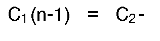

- Transformator nach Anspruch 2, dadurch gekennzeichnet, daß C₁ = C₂ und

- Transformator nach Anspruch 1, dadurch gekennzeichnet, daßa) die Sekundärwicklung (3) zwei Spulen (55, 57, 59, 61) enthält, die je aus einem bifilaren, in Form eines Solenoids gewickelten Teilspulenpaars bestehen, wobei ein Ende der ersten Teilspule (55, 59) mit dem entgegengesetzten Ende der zweiten Teilspule (57, 61) galvanisch verbunden ist, so daß die nicht miteinander verbundenen Enden der beiden Teilspulen im Betriebszustand gleiche und entgegengesetzte Spannungen in bezug auf die miteinander verbundenen Enden führen;b) die erste Primärspule (63) mit der ersten Sekundärspule (55, 57) und die zweite Primärspule (71) mit der zweiten Sekundärspule kapazitiv gekoppelt sind;c) die Windungszahlen der ersten und der zweiten Primärspule sich wie q/r verhalten, wobei die Bedingung erfüllt ist, da


- Transformator nach Anspruch 4, dadurch gekennzeichnet, daß C₁ = C₂ und q = r sind.
Applications Claiming Priority (2)
| Application Number | Priority Date | Filing Date | Title |
|---|---|---|---|
| NL8702133 | 1987-09-09 | ||
| NL8702133A NL8702133A (nl) | 1987-09-09 | 1987-09-09 | Transformator. |
Publications (2)
| Publication Number | Publication Date |
|---|---|
| EP0307036A1 EP0307036A1 (de) | 1989-03-15 |
| EP0307036B1 true EP0307036B1 (de) | 1993-07-28 |
Family
ID=19850582
Family Applications (1)
| Application Number | Title | Priority Date | Filing Date |
|---|---|---|---|
| EP88201861A Expired - Lifetime EP0307036B1 (de) | 1987-09-09 | 1988-08-31 | Transformator |
Country Status (6)
| Country | Link |
|---|---|
| US (1) | US5093613A (de) |
| EP (1) | EP0307036B1 (de) |
| JP (1) | JPS6472514A (de) |
| KR (1) | KR890005777A (de) |
| DE (1) | DE3882626T2 (de) |
| NL (1) | NL8702133A (de) |
Families Citing this family (8)
| Publication number | Priority date | Publication date | Assignee | Title |
|---|---|---|---|---|
| NL8901961A (nl) * | 1989-07-28 | 1991-02-18 | Koninkl Philips Electronics Nv | Generator voor het opwekken van een elektrische spanning. |
| US5392020A (en) * | 1992-12-14 | 1995-02-21 | Chang; Kern K. N. | Flexible transformer apparatus particularly adapted for high voltage operation |
| EP0771012A3 (de) * | 1994-08-24 | 1998-02-25 | Yokogawa Electric Corporation | Transformator mit gedruckten Spulen |
| EP0698896B1 (de) * | 1994-08-24 | 1998-05-13 | Yokogawa Electric Corporation | Gedruckte Spule |
| US5736916A (en) * | 1995-06-07 | 1998-04-07 | Kollmorgen Corporation | High frequency pulse transformer for an IGBT gate drive |
| US5666047A (en) * | 1995-10-05 | 1997-09-09 | The United States Of America As Represented By The Secretary Of The Navy | Dielectric transformer |
| WO2010015105A1 (en) * | 2008-08-06 | 2010-02-11 | Iwatt Inc. | Power converter using energy stored in leakage inductance of transformer to power switch controller |
| WO2023288248A2 (en) * | 2021-07-13 | 2023-01-19 | Georgia Tech Research Corporation | Soft switching solid state transformers implementing voltage stress mitigation techniques |
Family Cites Families (12)
| Publication number | Priority date | Publication date | Assignee | Title |
|---|---|---|---|---|
| US1702771A (en) * | 1926-05-14 | 1929-02-19 | Rca Corp | Amplifying transformer |
| FR766585A (fr) * | 1933-03-31 | 1934-06-30 | Soc Indep Telegraphie Sans Fil | Transformateur à capacités internes neutralisées |
| US3210706A (en) * | 1964-03-25 | 1965-10-05 | Westinghouse Electric Corp | Electrical inductive apparatus having interleaved windings for providing a predetermined capacitive effect |
| US3299384A (en) * | 1964-07-01 | 1967-01-17 | Ibm | Wide-band transformer having neutralizing winding |
| US3683271A (en) * | 1970-06-23 | 1972-08-08 | Tatsuo Kobayashi | Power supply filter for noise suppression |
| US3688232A (en) * | 1971-02-16 | 1972-08-29 | Gabor Szatmari | Capacitive inductive winding |
| US3886434A (en) * | 1973-09-07 | 1975-05-27 | Warwick Electronics Inc | Flyback transformer |
| DE2444894A1 (de) * | 1974-09-19 | 1976-04-08 | Siemens Ag | Transformator mit galvanischer trennung der primaer- und sekundaerseite |
| DE2446605A1 (de) * | 1974-09-30 | 1976-04-08 | Siemens Ag | Induktives funktionselement |
| AU511007B2 (en) * | 1975-06-11 | 1980-07-24 | Sony Corporation | Transformer |
| US4581573A (en) * | 1984-01-13 | 1986-04-08 | Bbc Brown, Boveri & Company, Limited | Static converter transformer with harmonic filter |
| JPS61170008A (ja) * | 1985-01-23 | 1986-07-31 | Murata Mfg Co Ltd | フライバックトランス |
-
1987
- 1987-09-09 NL NL8702133A patent/NL8702133A/nl not_active Application Discontinuation
-
1988
- 1988-08-31 DE DE88201861T patent/DE3882626T2/de not_active Expired - Fee Related
- 1988-08-31 EP EP88201861A patent/EP0307036B1/de not_active Expired - Lifetime
- 1988-09-01 US US07/239,575 patent/US5093613A/en not_active Expired - Fee Related
- 1988-09-02 JP JP63220262A patent/JPS6472514A/ja active Pending
- 1988-09-08 KR KR1019880011572A patent/KR890005777A/ko not_active Application Discontinuation
Also Published As
| Publication number | Publication date |
|---|---|
| NL8702133A (nl) | 1989-04-03 |
| US5093613A (en) | 1992-03-03 |
| KR890005777A (ko) | 1989-05-17 |
| EP0307036A1 (de) | 1989-03-15 |
| DE3882626D1 (de) | 1993-09-02 |
| DE3882626T2 (de) | 1994-02-03 |
| JPS6472514A (en) | 1989-03-17 |
Similar Documents
| Publication | Publication Date | Title |
|---|---|---|
| US4922156A (en) | Integrated power capacitor and inductors/transformers utilizing insulated amorphous metal ribbon | |
| EP0307036B1 (de) | Transformator | |
| US5331255A (en) | High voltage power supply | |
| EP0410526B1 (de) | Generator zum Erzeugen einer elektrischen Spannung | |
| US3160838A (en) | Electric transformers | |
| US4571570A (en) | Winding for static induction apparatus | |
| CA2347690A1 (en) | Transformer winding | |
| US4042900A (en) | Electrostatic shielding of disc windings | |
| US3466584A (en) | Winding for a stationary induction electrical apparatus | |
| JPH04133408A (ja) | 平面トランス | |
| US1940864A (en) | Electrical apparatus | |
| US3560902A (en) | Method of providing static shielding of transformer windings | |
| EP0450448A1 (de) | Transformator in Flachbauweise | |
| US2586352A (en) | High-frequency transformer | |
| US4317096A (en) | Electrostatic shielding of nonsequential disc windings in transformers | |
| US4243966A (en) | Electrostatic shielding of nonsequential disc windings in transformers | |
| JPH0311534B2 (de) | ||
| US20240128009A1 (en) | Magnetic device | |
| JPS58166708A (ja) | 変圧器巻線構造 | |
| JPS63263708A (ja) | 高圧変圧器 | |
| JP3444567B2 (ja) | ガス絶縁誘導機器 | |
| JPS60210818A (ja) | 誘導電器巻線 | |
| JPS607456Y2 (ja) | 誘導電器巻線 | |
| JPS62262411A (ja) | 高圧単巻変圧器 | |
| JPS5861612A (ja) | 誘導電器巻線 |
Legal Events
| Date | Code | Title | Description |
|---|---|---|---|
| PUAI | Public reference made under article 153(3) epc to a published international application that has entered the european phase |
Free format text: ORIGINAL CODE: 0009012 |
|
| AK | Designated contracting states |
Kind code of ref document: A1 Designated state(s): DE ES FR GB IT |
|
| 17P | Request for examination filed |
Effective date: 19890831 |
|
| 17Q | First examination report despatched |
Effective date: 19910910 |
|
| GRAA | (expected) grant |
Free format text: ORIGINAL CODE: 0009210 |
|
| AK | Designated contracting states |
Kind code of ref document: B1 Designated state(s): DE ES FR GB IT |
|
| PG25 | Lapsed in a contracting state [announced via postgrant information from national office to epo] |
Ref country code: IT Free format text: LAPSE BECAUSE OF FAILURE TO SUBMIT A TRANSLATION OF THE DESCRIPTION OR TO PAY THE FEE WITHIN THE PRE;WARNING: LAPSES OF ITALIAN PATENTS WITH EFFECTIVE DATE BEFORE 2007 MAY HAVE OCCURRED AT ANY TIME BEFORE 2007. THE CORRECT EFFECTIVE DATE MAY BE DIFFERENT FROM THE ONE RECORDED.SCRIBED TIME-LIMIT Effective date: 19930728 Ref country code: ES Free format text: THE PATENT HAS BEEN ANNULLED BY A DECISION OF A NATIONAL AUTHORITY Effective date: 19930728 |
|
| REF | Corresponds to: |
Ref document number: 3882626 Country of ref document: DE Date of ref document: 19930902 |
|
| ET | Fr: translation filed | ||
| PLBE | No opposition filed within time limit |
Free format text: ORIGINAL CODE: 0009261 |
|
| STAA | Information on the status of an ep patent application or granted ep patent |
Free format text: STATUS: NO OPPOSITION FILED WITHIN TIME LIMIT |
|
| 26N | No opposition filed | ||
| PGFP | Annual fee paid to national office [announced via postgrant information from national office to epo] |
Ref country code: GB Payment date: 19940728 Year of fee payment: 7 |
|
| PGFP | Annual fee paid to national office [announced via postgrant information from national office to epo] |
Ref country code: FR Payment date: 19940825 Year of fee payment: 7 |
|
| PGFP | Annual fee paid to national office [announced via postgrant information from national office to epo] |
Ref country code: DE Payment date: 19941026 Year of fee payment: 7 |
|
| PG25 | Lapsed in a contracting state [announced via postgrant information from national office to epo] |
Ref country code: GB Effective date: 19950831 |
|
| PG25 | Lapsed in a contracting state [announced via postgrant information from national office to epo] |
Ref country code: FR Effective date: 19960430 |
|
| GBPC | Gb: european patent ceased through non-payment of renewal fee |
Effective date: 19950831 |
|
| PG25 | Lapsed in a contracting state [announced via postgrant information from national office to epo] |
Ref country code: DE Effective date: 19960501 |
|
| REG | Reference to a national code |
Ref country code: FR Ref legal event code: ST |