EP0300916B1 - Cell for the modulation of light - Google Patents
Cell for the modulation of light Download PDFInfo
- Publication number
- EP0300916B1 EP0300916B1 EP88401914A EP88401914A EP0300916B1 EP 0300916 B1 EP0300916 B1 EP 0300916B1 EP 88401914 A EP88401914 A EP 88401914A EP 88401914 A EP88401914 A EP 88401914A EP 0300916 B1 EP0300916 B1 EP 0300916B1
- Authority
- EP
- European Patent Office
- Prior art keywords
- layer
- electrode
- light
- counter
- modulating cell
- Prior art date
- Legal status (The legal status is an assumption and is not a legal conclusion. Google has not performed a legal analysis and makes no representation as to the accuracy of the status listed.)
- Expired - Lifetime
Links
Images


Classifications
-
- G—PHYSICS
- G02—OPTICS
- G02F—OPTICAL DEVICES OR ARRANGEMENTS FOR THE CONTROL OF LIGHT BY MODIFICATION OF THE OPTICAL PROPERTIES OF THE MEDIA OF THE ELEMENTS INVOLVED THEREIN; NON-LINEAR OPTICS; FREQUENCY-CHANGING OF LIGHT; OPTICAL LOGIC ELEMENTS; OPTICAL ANALOGUE/DIGITAL CONVERTERS
- G02F1/00—Devices or arrangements for the control of the intensity, colour, phase, polarisation or direction of light arriving from an independent light source, e.g. switching, gating or modulating; Non-linear optics
- G02F1/01—Devices or arrangements for the control of the intensity, colour, phase, polarisation or direction of light arriving from an independent light source, e.g. switching, gating or modulating; Non-linear optics for the control of the intensity, phase, polarisation or colour
- G02F1/15—Devices or arrangements for the control of the intensity, colour, phase, polarisation or direction of light arriving from an independent light source, e.g. switching, gating or modulating; Non-linear optics for the control of the intensity, phase, polarisation or colour based on an electrochromic effect
- G02F1/153—Constructional details
- G02F1/1533—Constructional details structural features not otherwise provided for
Definitions
- the invention relates to a cell for the modulation of light, in particular for the variable reflection of light, the variable transmission of light, the display of signals and images such as for example alphanumeric information, graphics and other optical information.
- a cell for the modulation of light in particular for the variable reflection of light, the variable transmission of light, the display of signals and images such as for example alphanumeric information, graphics and other optical information.
- electro-optical devices in particular panels, screens and display devices, windows, display cases, screens, windshields, glasses, these being of variable transparency, light valves, shutters, variable reflection mirrors, memories, etc ...
- electrochromic processes use the reversible change in color and / or optical density obtained by electrochemical redox of a so-called electrochromic material whose oxidized form and reduced form are colored and / or of different optical densities.
- Electrochromic light modulation processes have a set of remarkable characteristics for many applications: low control voltage, at most a few volts; low energy consumption; open circuit memory; relatively uncritical spacing between electrode and counter electrode. They also have additional characteristics which are particularly advantageous for display devices: very high contrast, even in lateral vision at a high angle; excellent visibility by reflection in conditions of strong illumination such as outside in strong sunlight; extended gray scale; wide operating temperature range, often extending to low temperatures.
- the low control voltage allows the use of low-cost electronic control and addressing means.
- the low energy consumption allows applications where autonomous operation (on batteries or accumulators) is required.
- an elementary cell of a light modulation, electrochromic, device of the prior art is a cell sealed (individually or in combination with other cells) in a strictly sealed manner vis-à-vis from the outside ambient atmosphere.
- This cell generally includes a transparent front electrode deposited on a transparent plate of glass or plastic, an electrochromic material often in the form of a thin layer deposited on the transparent electrode, an interval filled with electrolyte, a counter-electrode (also transparent if the device operates by transmission) and electrical connection conductors from each electrode to the electronic control means outside the cell. It also more often than not includes a specific separator intended to maintain between the electrode and the counter-electrode a gap of constant thickness intended to contain the electrolyte.
- At least the front electrode and / or the layer of electrochromic material are delimited so as to define the shape required for the corresponding image point or image segment.
- a strictly watertight seal is necessary to avoid the loss (by leakage, evaporation, in particular, as the case may be) of constituents of the interior medium, in particular constituents of the electrolyte, and / or to prevent entry into the cell.
- constituents of the external ambient atmosphere for example oxygen, carbon dioxide, humidity, various contaminating bodies
- the sealing problem is all the more important since the cell must allow the sealed passage of the conductors which connect the front electrode and the counter-electrode to the external electronic means.
- the sealing joints which must be compatible with the different materials used, are subject to mechanical stresses resulting in particular from the differences between the expansion coefficients of these materials; this problem is aggravated when the dimensions of the device are increased: to the stresses of thermal origin which can increase due to asymmetries of exposure to heat sources can be added stresses of mechanical origin due to the vibrations to which a panel of large dimensions is naturally exposed and to the interaction with the fixing and holding structure of the panel.
- electrochromic solids are generally solids insoluble in the two oxidation states between which they change color; these solids are electrically insulating or weakly conductive. Mention may be made, among others among inorganic materials in particular: WO3, MoO3, V2O5, Nb2O5, IrO index x (an extensive list is given for example in the document US Pat. No. 3,704,057) and, among organic materials: diphtalocyanine from Lu, from Yb , especially.
- electrochromic solids must generally be used by depositing a thin layer on the transparent electrode using expensive vacuum deposition techniques (evaporation under vacuum, sputtering in particular). Their color change is generally colorless or from a first color to a second other color: colorless to blue for WO3 and MoO3, yellow to green for V2O5, colorless to blue or blue-black for IrO index x, green to red for lutetium diphthalocyanine.
- the reversible electrodeposition of metals from an electrolytic solution has been the subject of various works, in particular with liquid organic electrolytes because of the corrosion problems and harmful parasitic reactions to the stability and to the lifetime encountered with aqueous electrolytes.
- Y. Duchene et al. (cited article) describe a display cell using as electrolyte methanol or acetonitrile containing silver iodide and sodium iodide.
- the silver ions are reduced to a silver film with high contrast.
- the optical density depends, for the same electrical charge, on the density of current used, and heterogeneities appear on the film deposited after a certain number of deposition-redissolution cycles.
- the cell does not have a write voltage threshold and therefore does not lend itself to multiplexed matrix writing.
- the area of the transparent electrode corresponding to the display must be delimited inside the cell using an insulating layer engraved according to the drawing of the area in question.
- the use of glass sealing technology is indicated as one of the conditions of reliability, confirming the importance of strictly watertight sealing.
- a neighboring cell described by I. Camlibel et at. contains silver iodide and potassium iodide in dimethyl sulfoxide and produces a specular or bright red deposit depending on the conditions.
- Electroactive polymers (redox):
- Recent work relates to polymers such as polyaniline, polyacetylene, polypyrrole, polythiophene, in particular which, in a thin layer on a transparent electrode, can change color (for example from red to blue for polythiophene) according to their state oxidation.
- These materials which are generally quite unstable, or easily alterable, have a short service life and allow only a very small number of operating cycles to be achieved.
- liquid electrolyte for example an aqueous electrolyte such as an aqueous solution of sulfuric acid (document FR 76.26282), or an organic electrolyte such as a solution of lithium perchlorate in propylene carbonate (document Yoshiro Mori, art. cited).
- aqueous electrolyte such as an aqueous solution of sulfuric acid (document FR 76.26282)
- organic electrolyte such as a solution of lithium perchlorate in propylene carbonate (document Yoshiro Mori, art. cited).
- This electrolyte which cannot generally be common to several cells for electrical reasons, requires an individual confinement in each cell which must include a non-deformable electrolytic compartment.
- inorganic solids with ionic conductivity have also been used, such as for example beta alumina (document M. Green et al., Solid State Ionics 3/4, 1981 , pages 141 to 147, North-Holland), or alternatively ion-conducting polymers, such as for example solid solutions of lithium perchlorate in polyethylene oxide (document FR 83.09886).
- beta alumina document M. Green et al., Solid State Ionics 3/4, 1981 , pages 141 to 147, North-Holland
- alternatively ion-conducting polymers such as for example solid solutions of lithium perchlorate in polyethylene oxide (document FR 83.09886).
- solid electrolytes exhibit, at ambient or ordinary temperatures, only a generally very low ionic conductivity, considerably penalizing the speed of writing and erasing which may require several seconds or even much more.
- the counter-electrode is often of complex and costly structure and manufacture, because of the functions which it can have to perform. simultaneously: auxiliary redox function, maintenance of a constant and even determined electrode potential, high load capacity, reversibility, etc., while being capable of a high number of cycles without degradation.
- a counter electrode has been produced comprising a second layer of an electrochromic solid modified so as to have low electrochromicity and deposited on a transparent electrode (document US 4,278,329).
- Another known counter-electrode is a sheet of paper formed using acrylic fibers, a binder and carbon powder, in which an electrochromic solid is also incorporated (document US Pat. No. 4,088,395).
- Another counter electrode, the electrode potention of which is adjustable comprises carbon powder, a binder and mixtures of the depolarisers W18O49 and V6O13 in adjustable proportions (document Yoshiro Mori, article cited).
- the electrochromic material and the process for its implementation aim to obtain a mark (signal or image) essentially stable over time.
- the present invention relates to a cell for modulating light and to a method of manufacturing the same which avoid the drawbacks of known cells.
- a light modulation cell is defined by claim 1.
- This cell allowing the writing of at least one image point or image segment, maintenance in the written state of such an image point or image segment, reversibly, the erasure of such an image point or image segment, and maintenance in the state erased from this image point or image segment, the writing of an image point or image segment being defined as the increase in optical density in the region of the interface between the working electrode and the layer or portion of layer of material and the erasure of an image point or image segment being defined as the reduction or disappearance of the increase in optical density obtained during writing.
- this cell is also characterized in that the counter-electrode is transparent or substantially transparent so that the cell can operate in particular by transmission.
- the counter electrode is opaque, the cell functioning by reflection. It further comprises a reflecting and / or masking and / or diffusing element placed between the electrode and the counter-electrode.
- a working electrode and / or a counter electrode has a self-supporting structure or is supported by a self-supporting substrate. The substrate is transparent or substantially transparent when the electrode associated with it is itself transparent or substantially transparent.
- the layer of electrolytic material has a thickness of between in particular a few micrometers and several tens of micrometers.
- the layer of electrolytic material has adhesive properties, in particular a tacky feel or a contact tacky.
- a layer of electrolytic material is continuous.
- a layer of at least the electrolytic material is in grains or juxtaposed particles maintained by themselves or by means of a binder. It further comprises specific additional means for maintaining its cohesion and the permanence of the electrical contacts; and / or specific additional means for isolating and protecting its constituent elements from the ambient atmosphere; and / or a specific spacer.
- the layer of electrolytic material is substantially rigid and the cell has no specific spacer between the two electrodes.
- the layer of electrolytic material has a tacky or tacky contact feel and, on the other hand, the cell is devoid of specific additional means of maintaining cohesion.
- a layer of electrolytic material has a permanent ionic conductivity, including in contact with the external ambient atmosphere and, on the other hand, the cell is devoid of specific means ensuring its sealing against humidity .
- An image point or image segment is determined in shape, size and position exclusively by the intersection of orthogonal projections, on a screen surface, of areas given to the working electrode, to the counter-electrode and to the layer of electrolytic material.
- the area of one of the components is determined in size and position form by the intersection of the orthogonal projections, on a screen surface of the areas of the two other components.
- the areas of two components are identical and superimposed and their common orthogonal projection on the third component is included in the area of the latter.
- a layer is first formed on at least one electrode and this layer is then given its solid consistency, in particular by evaporation, heat treatment, crosslinking, vulcanization.
- the layer is first given its solid consistency, in particular by evaporation, heat treatment, and the layer is then formed on at least one electrode. It comprises a step consisting in forming at least one layer of electrolytic material on one of the two electrodes and another, subsequent step consisting in applying this layer, by its free face, to the other electrode. It comprises a step consisting in forming at least a first layer on one of the two electrodes, another step consisting in forming at least a second layer on the other electrode and another subsequent step consisting in joining the first and second layers by their faces free.
- a layer is formed in a single pass (single layer) or in several passes (composite layer) of identical or different formative compositions, successively or not.
- the layer of electrolytic material is given a surface or contact tack.
- the electrolytic material and the electrode are directly applied in contact with each other; either the electrolytic material is first applied to an intermediate and temporary substrate, in particular a non-stick surface finish, and the layer of electrolytic material is then transferred from the substrate to the electrode considered.
- the formative composition is applied in one or more layers of total thickness preferably between a few micrometers and several hundred micrometers depending in particular on its water content, so as to obtain a layer of electrolytic material of thickness preferably between a few micrometers and several tens of micrometers.
- the formative composition comprises at least the constituents of the electrolytic material and a supplement of water, and optionally agents for maintaining stability and / or conservation and / or facilitating the application in layer of the formative composition.
- the viscosity of the fluid forming composition is adjusted to a value suitable for a particular method of formation and / or application in a layer by evaporation of part of its water or by addition of additional water. Areas electric current supply lines are distributed so as to obtain a current density as uniform as possible inside the image point or image segment.
- Image point or “image segment”: Delimited area or surface whose optical density is likely to be increased (that is to say, to acquire in vision by reflection a coloration or a blackening and / or partially or completely opacify in vision by transmission if it is transparent) and, conversely, reduced to return in particular to its original appearance (original reflection and / or original transparency).
- image point is preferably reserved for a small surface (for example relative to the surface of a screen of a light modulation device which contains a multiplicity thereof), often of circular, square or slightly rectangular shape, repeated, on the surface of a display device screen which contains a multiplicity thereof, identically to itself according to the nodes of a network (for example square, centered square, compact hexagonal, in particular) which occupies regions or the entire screen area.
- a network for example square, centered square, compact hexagonal, in particular
- image segment is preferably reserved for a surface which may be large (for example relative to the surface of a screen of a light modulation device which contains a multiplicity thereof), of any shape but often elongated, associated, on the surface of a screen of a display device which contains a multiplicity thereof, with other image segments of the same shape and / or of different shapes according to specific geometric arrangements, such as, for example, the well-known arrangement of seven segments allowing the representation of the numbers from 0 to 9 by coloring or selective opacification of suitable combinations of these segments.
- Elementary light modulation cell or “elementary light modulation device” (or abbreviated cell, elementary device): Complete structure necessary for the creation of an image point or image segment and for its operation reversible when the cell is electrically controlled.
- An elementary electrochromic modulation cell comprises at least, as components, suitably arranged and associated, a first transparent electrode or working electrode, a second electrode or counter electrode (transparent or not, depending on whether the image point or image segment is observed by light transmission or by reflection), an ion conductor or electrolytic material placed between the electrodes, electrochromism means and means of electrical connection to an external source of electric voltage allowing the control of the cell and, if an elementary cell is part of a multiplicity of elementary cells in the same display device , addressing means (direct, multiplexed, etc.) making it possible to control it selectively.
- the expression “elementary modulation cell” is used instead to designate the minimum structure essential for obtaining an image point or image segment in accordance with the invention and the expression “ elementary device "to designate a device comprising a single elementary cell and extrinsic or peripheral components or constituents necessary for its operation either as a unitary device, or combined with one or more other elementary devices in a compound device having a plurality of associated cells.
- extrinsic constituents or components are, for example, electrical connections associated with the electrodes; means for masking the periphery of the cell; a transparent substrate for the transparent electrode.
- “Autonomous light modulation device” At least one basic modulation device as well as the other specific components allowing the device to be used as an autonomous unit, among which in particular: mechanical supports or substrates giving the autonomous device structural rigidity; case; encapsulation; internal electrical connections to the autonomous device; connector (s) or connection area (s) to which or to which are connected, by means of internal electrical connections, the elementary devices of the autonomous device, making it possible to easily connect the latter to the control and addressing electronics and the associated source of electrical energy; printed circuit which can possibly function, individually or in combination, in particular of mechanical support, connector or connector support, support of a part of the associated electronics.
- Such an autonomous device can for example be a device commonly called a device, display panel or screen or more generally a any of the most diverse electro-optical devices.
- “Screen area of a display device” The area that includes, frames and connects all the image points and / or image segments of the device.
- image point (or image segment) and elementary modulation cell is also understood to mean the colorable, densifiable or opacifiable area and the corresponding elementary cell, whatever their shape and size, of light modulation devices which are not actual display devices, for example variable light transmission or variable light reflection devices, and often only have one elementary cell in particular and for example windows, display cases, screens, windshields, spectacles, with variable transparency, light valves, shutters, mirrors with variable reflection, light amplification devices.
- Solid consistency The consistency of a material having, in the absence of applied external constraints, the appearance of a solid.
- the solid consistency includes, without limitation, the consistency of a pasty medium of very high viscosity, the consistency of a thixotropic fluid in the resting state, the consistency of a gel or of a gelled medium, the consistency of '' a plasticized polymer film.
- Frm-forming The ability to form a film in the existing blend system, which also includes the other constituents of the blend.
- “Primarily water-soluble” Water-soluble at least before incorporation into the electrolytic material or into a composition forming an electrolytic material. Once the electrolytic material has been formed, the original water-solubility of the resin may be partially or totally lost, reversibly or irreversibly, for example, following crosslinking by a crosslinking agent.
- Layer a film or film sheet of homogeneous, heterogeneous or composite material, generally having an extended surface relative to its thickness and preferably but not limitatively at least substantially constant thickness.
- a layer can be simple or composite when it itself comprises several layers.
- Such a layer can be of unfractionated extent or, on the contrary, can be divided into layer portions. In the rest of the text, the term layer is used for this general meaning and any one of those of detail.
- Thin thickness of a layer of the electrolytic material A thickness preferably between a few micrometers and several tens of micrometers.
- Thin thickness of an electrode a thickness preferably between a few tens of nanometers (hundreds of Angstroems) and several hundred micrometers.
- Thin thickness of a modulation device A small thickness in front of its surface, preferably between a few micrometers and several hundred micrometers, the thickness of a substrate not being able to be understood.
- Alloy The association or combination of several different metallic species, whether a solid solution, an intermetallic compound, a juxtaposition of crystallites of each metal or any other form of association or combination, obtained by codeposition of several metals.
- the electrolytic material used in the elementary cell has the characteristics that it has an ionic conductivity; that it has plastic or viscoelastic deformability; that it is conformable in a continuous thin layer; and that it has at least the functions not only of participating in the writing or erasing of an image point or image segment, but also of allowing the passage of electric current between the working electrode and the counter electrode during writing and during erasure, and this by cathodic reduction of depositable metal ions which it contains, in combination with the working electrode, (writing phase); by anodic oxidation and reincorporation in the original state of the metal ions produced by this oxidation, in combination with the working electrode, (erasure phase); and finally by transporting in each direction, respectively, electric charges in ionic form, between the working electrode and the counter-eclectrode, in an amount equal to the electric charges injected in electronic form into the electrolytic material by the working electrode during l 'writing; and electrical charges removed in electronic form from the electrolytic material by
- An electrochromic method of modulating light, by reflection or transmission implemented by the cell and the material thus described comprises the following combination of phases: at least one such electrolytic material is produced; at least one layer of at least one electrolytic material with a thickness between in particular a few micrometers and several tens of micrometers is produced; the electrodes of the cell are placed in contact with the faces of said layer of electrolytic material; during at least one writing phase, of a certain duration, a negative electrical voltage is applied to the working electrode with respect to that of the counter electrode, so that during this writing phase is written at least one image point or image segment; during at least one erasing phase, subsequent to a writing phase, an electric current is passed between the electrodes, the direction of which is opposite to that of the electric current of the writing phase, so that, during this erasure phase, the previously written image point or image segment is erased; the process being repetitive and can include several couples of a writing phase and an erasing phase.
- the image point or image segment 5 written is on the one hand a surface delimited by a remarkably sharp outline, corresponding to the intersection of the orthogonal projections, on the screen surface of the cell, of the areas of the two electrodes 2, 4 and of the layer of electrolytic material 3, on the other hand, of dark, matt and amorphous appearance, very different from that of a conventional metallic deposit: clear, shiny, and crystalline, close to that of a "black" of metal and which can go so far as to have the appearance of a black of printing ink, as described below.
- the image point or image segment 5 written reproduces exactly the shape of the counter-electrode 4, although it is formed at a certain distance from the latter, without any blurred or diffuse outline being observed as might be expected.
- the image point or image segment 5, once written, does not diffuse beyond its outline and is not diluted by the non-colored or densified periphery. This characteristic is illustrated schematically in FIG. 5.
- the delimitation of the contour of each image point or image segment 5 which can be reduced to the intersection of the areas of a transparent electrode 2 and a counter electrode 4 both elongated and of general directions perpendicular to each other, the electrolytic material 3 having an area encompassing the minus this intersection, lends itself to constructions of extreme simplicity and makes it possible to obtain image points or image segment 5 of very small dimension as well as to reduce to a minimum value the intervals between the image points or segment d 'adjacent images.
- This variant is shown diagrammatically in FIG. 9, in the particular case where the electrolytic material 3 is in the form of bands coaxial with the counter-electrodes 4 and projecting slightly laterally from these. This variant is intended for so-called hardware display panels.
- the optical density of the image point or image segment 5 is uniform within its contour up to large dimensions of this image point or image segment, of the order of one to several square centimeters, without special precautions.
- a suitable geometry of the zones or points of supply of current draw that is to say of the zones of current supply, electrical respectively 11 and 12 on the working electrode 2 and, optionally, on the counter electrode 4, is necessary to ensure a current density sufficiently uniform to obtain a uniform optical density.
- the mark obtained with a writing style is always very dense by reflection and opaque by transparency and the fact of varying the electric charge when the writing style forming cathode is stationary during the registration of 'a point, or to vary the current density when the style moves to write a line, has the only effect of varying the diameter of the point or the width of the line but not to affect its optical density as in the present invention.
- the writing process can be implemented in such a way as to present a well-defined and high-value electric voltage threshold, that is to say by applying a writing electric voltage below this threshold to a cell.
- a writing electric voltage below this threshold to say by applying a writing electric voltage below this threshold to a cell.
- elementary 1 the image point or image segment 5 cannot be written.
- Such an electrical write voltage threshold is essential for the multiplexed addressing of a matrix display device.
- the erasure of the written image point or image segment 5 is obtained by circulating in the elementary cell 1 a current of direction opposite to that of the write current (write phase), this which is obtained in particular generally either by applying to the electrodes 2, 4 an electric voltage in the opposite direction to that of the writing voltage; or, in the case where the cell has an electromotive force, by simple short-circuit.
- the modulation process thus described makes it possible reversibly and repeatedly to write and erase image points or segments of images, which document FR 2 504 290, already mentioned, does not provide.
- an image point or image segment 5 is written by cathodic reduction in the region of the working electrode interface 2-layer of electrolytic material 3, of metal ions present in the layer of electrolytic material 3 in metal or metal alloy which electrocrystallizes according to a particular mode having remarkable characteristics of optical density, uniformity, contour precision, gray scale and absence of diffusion or dilution, etc ... described above.
- the image point or image segment 5 is deleted by anodic oxidation of the deposit of metal or metal alloy thus formed.
- the electrolytic material is therefore already characterized at least by this double function of ensuring this writing and allowing this erasure.
- the metal deposit formed in the interfacial region is capable of being redissolved by anodic oxidation, without any residual deposit remaining and without the massive reinjection of the metal ions produced by this oxidation in the electrolytic material. does not produce parasitic or harmful phenomena or processes (such as for example a local flocculation or "salting out" of the film-forming polymer) as might be expected.
- the cathodic deposition of metal or alloy according to the particular mode of electrocrystallization observed and its dissolution by anodic oxidation are obtained with layers of electrolytic material containing, depending on the case, a single metal or several metals taken from most of the metals cathodically depositable alone or co-depositable with several or even not depositable alone but co-depositable with others, from an aqueous solution of their simple or complex ions or a combination of them, in particular: zinc, cadmium lead, silver, copper, iron, cobalt, nickel, tin, indium, platinum, palladium, gold, bismuth, antimony, tellurium, manganese, thallium, selenium, gallium, arsenic, mercury, chromium, tungsten, molybdenum, associated with a large number of polymer resins water-soluble film formers.
- the actual crystal structure of the developed metallic deposit which appears to be embedded in the network of the polymer resin, could be that of a highly divided state, particularly with regard to otpic appearance and density, one of the hypotheses being that of a multidendritic growth along the molecular chains of the resin.
- the invention is not linked to the hypotheses and assumptions thus stated.
- the electrolytic material can, without disadvantage for obtaining the optical densification of the image point or image segment with the characteristics mentioned above as well as without disadvantage for its erasure, contain in addition to the electrodepositable cations already mentioned cations of metals which are not electrodepositable from an aqueous solution, in particular in a significant proportion. This feature provides greater flexibility for the formulation of electrolytic materials that better meet the specifications of different particular applications.
- the inscription of the marks on the recording medium is inhibited and replaced by a metallic deposit on the cathode constituted by the writing electrode and / or by a release of hydrogen, when the layer of electrochromic material contains a significant proportion of metal cations which cannot be electrodeposited from an aqueous solution, such as the alkalis (with the exception of the ammonium ion), the alkaline earths in particular.
- an aqueous solution such as the alkalis (with the exception of the ammonium ion), the alkaline earths in particular.
- the presence of a significant amount of non-electrodepositable metal cations has no inhibitory effect.
- the voltages necessary for writing are at most a few volts (whereas according to document FR 2,504,290, the voltages used are generally included in a range going from d '' about a few Volts to several tens of Volts).
- a layer of electrolytic material used in the invention is generally a continuous layer, that is to say a non-granular layer, transparent or substantially transparent. Depending on the nature of the ions it contains, it can be colorless or colored.
- the layer of electrolytic material is left in this transparent form or substantially transparent and as lightly colored as possible, unless it also constitutes a colored filter, for example for the production of colored dormers with variable transmission or color display devices.
- a masking and / or contrasting pigment compatible with the other constituents of the electrolytic material such a pigment has the effect of masking the counter electrode if this does not constitute a background of color and / or of satisfactory contrast, to attenuate a possible colored shade of the electrolytic material if such a coloration exists because of the composition and is not desirable and to constitute a background offering the most desirable contrast with the black appearance of the image point or written image segment.
- a white pigment such as titanium dioxide, especially in the rutile and anatase crystalline forms, dispersed in particulate form in the layer of electrolytic material or in only a fraction of the thickness of this layer makes it possible to obtain a particularly white background.
- colored pigments can be used, alone or as a mixture with a white pigment.
- the color of a colored pigment or a dye present in the electrolytic material gradually fades to black with practically no residual coloration when the optical density of an image point or segment d is gradually increased. 'picture. Everything happens as if the reflected or transmitted colored radiation (as the case may be) was filtered by the neutral gray screen produced by the written image point or image segment.
- This remarkable feature allows the production of multi-color display devices by three-color additive synthesis with three electrolytic materials each colored according to one of the three primary colors.
- the electrolytic material used in the invention may comprise, depending on the case, the ions of a single metal or of several metals taken from most of the cathodically depositable metals alone or codeposited in several. It is thus possible, depending on the case, to change the conditions for obtaining the deposit of only one of these metals and / or to modify the particularities of writing or erasing and / or the appearance of such a deposit or even obtaining by cathodic reduction an alloy which may have an aspect and / or writing or erasing characteristics and / or particularities combining those individually deposited metals, but also present a completely new appearance and / or writing and erasing characteristics and / or particularities, for example, with regard to memory (i.e. the persistence of the coloring, densification or opacification of the image point or image segment in the absence of electric voltage imposed on the elementary cell).
- memory i.e. the persistence of the coloring, densification or opacification of the image point or image segment in the absence of electric voltage
- the water-soluble metal salt or the water-soluble mixture of metal salts is hygroscopic and preferably deliquescent in the presence of atmospheric humidity.
- a layer or a film of electrolytic material of a few micrometers to several tens of micrometers in thickness, not enclosed in a sealed enclosure permanently retains a high ionic electrical conductivity, until very low atmospheric humidity, which allows the elementary modulation cell to operate with a voltage of a few Volts at most.
- This high ionic electrical conductivity is due to the fact that with hygroscopic salts, the layer of electrolytic material, although it has the appearance and solid consistency of a dry layer, keeps a certain amount of water in equilibrium with atmospheric humidity.
- This internal water, in which the metal salts are dissolved in very high concentration, provides the layer of electrolytic material with a notable ionic conductivity which varies with atmospheric humidity but remains high up to its lowest contents, with a value which depends on the degree of hygroscopicity or deliquescence of the combination of salts chosen.
- composition of the electrolytic material it is possible to avoid sealing the elementary light modulation cell in a strictly watertight manner, unlike most of the electrochromic display devices of the prior art, which represents a considerable simplification of the manufacture of the cell or device and a reduction in its cost. Indeed, we can tolerate to a very large extent the effect of a penetration atmospheric humidity in the cell and that of a loss of water contained in the layer of electrolytic material. Surprisingly, one can also tolerate the effect of penetration of atmospheric oxygen into the cell.
- Protective insulation of the cell or of the device is desirable or even necessary, in the case of operation of the light modulation cell in extreme atmospheres and / or aggressive and / or corrosive, in order to limit or prevent the access of the external environment to the components of the cell or of the device.
- the impact on the structure, the manufacturing problems and the costs is very different from that of the obligation to have to provide each cell or group of cells or device with a seal or a strictly watertight protection capable of ensuring and to keep a strictly waterproof protective insulation despite the thermal or mechanical constraints to which the cell or device may be subjected.
- a layer of electrolytic material used in the invention which has a solid consistency in the absence of external stresses applied, presents, under the effect of such stresses, a plastic or viscoelastic behavior (the characteristics of which depend in particular on the nature of the polymer resin, the degree of crosslinking). This behavior is of great importance. On the one hand, it allows the layer of electrolytic material to be conformed to the flatness defects of one and / or the other electrode, as well as to a lack of parallelism between the two electrodes ensuring excellent physical contact and electric despite these faults.
- the physical properties mentioned above of the electrolytic material make it possible to considerably simplify the construction of a cell or device for modulating light, to reduce the requirements with regard to the constituent materials and components and to allow the realization in particular of very large billboards. Indeed, it is not necessary to provide a specific spacer intended to maintain between working electrode and counter-electrode a rigorous parallelism and a spacing specific.
- a layer of electrolytic material deposited by industrial techniques of application or coating generally known in themselves such as air gap, wire rod, squeegee, extrusion, calendering, screen printing, in particular is sufficient to constitute the spacer. and to define a spacing of sufficient precision.
- the support for the transparent working electrodes can be without disadvantage, for example, a stretched glass plate.
- Very large surface display panels comprising a multiplicity of elementary display cells
- the electrolytic material used in the invention has adhesive properties and more specifically a tacky feel (known as “tack”) or contact tights (known as “pressure sensitive adhesion”).
- tacky feel known as "tack”
- pressure sensitive adhesion Such resins can be in particular and without limitation hydroxyethylcellulose, polyvinylpyrrolidone, polyvinyl alcohol, or equivalent.
- the tacky surface may be greatly reduced or nonexistent; in these cases, the layer of electrolytic material is advantageously made up in a composite manner with three superimposed layers, the two outer layers of which are formulated with the aid of a suitable resin and contain no crosslinking agent or contrasting pigment, or little enough to not not affect the sticky feel, the inner layer 7 may be devoid of this sticky feel ( Figure 6).
- the existence of such a tacky or tacky surface touch also makes it possible to simplify the manufacture of the cells and light modulation device.
- the mechanical cohesion of each cell can be maintained by the sole properties of contact tacky of the layer of electrolytic material adhering to both the working electrode and the counter electrode, without it being necessary to provide additional external mechanical means to maintain the cell.
- the adhesion of the electrolytic material to the two electrodes (working and counter-electrode) ensures excellent physical and electrical contact of the electronic conductor and the ionic conductor at each interface without the need to apply and maintain a pressure on the cell and therefore without the need to provide mechanical means for this purpose.
- the combination of such contact tights and the plastic or viscoelastic deformability already mentioned makes it possible to produce large display panels which can have a very simple structure and which are not affected by thermal and mechanical deformations and vibrations. to which such panels may be subjected.
- an electrochemical reaction combined with that which occurs at the working electrode: an anodic oxidation if the other is a cathodic reduction, and vice versa.
- an auxiliary redox couple capable of reversibly passing from one of its terms to the other by electrochemical redox; in the absence of such a reversible auxiliary redox couple, the oxidation and reduction at the counter-electrode may involve the degradation of materials constituting the cell and / or the generation of gaseous species which disturb operation.
- the electrolytic material used in the invention already intrinsically contains at least one first auxiliary redox couple which is precisely the redox couple which is used at the working electrode: the metal ion (s) -metal or alloy couple .
- the same torque term is present at the working electrode and the counter electrode, while the operation requires the presence of conjugate terms.
- An auxiliary redox couple of this type allows a satisfactory operation by reflection if a masking pigment which conceals the counter electrode is incorporated into the electrolytic material.
- transmission operation with an electrolytic material which has remained transparent and a transparent counter-electrode, the removal of the visible deposit on one of the electrodes is accompanied by the formation of a visible deposit on the other electrode and the maximum transmission of the cell is reduced.
- the electrolytic material used in the invention may also intrinsically contain a second auxiliary redox couple, the reduced form of which is, on the one hand, water-soluble in the presence of the other water-soluble constituents of the material, and, on the other hand, colorless or slightly colored with concentrations used.
- a second auxiliary redox couple of this type allows satisfactory operation both in transmission and in reflection, avoiding in transmission the drawback mentioned above.
- this second auxiliary redox couple in the electrolytic material can have two origins: either when a simple or complex metal ion cathodically reducible in metal, introduced as such in the electrolytic material, can pass reversibly to a higher degree of oxidation Student ; this is the case, among others, of lead, silver, copper, iron, mercury, tin, in particular; for example, Cu (I), Fe (II), introduced to respectively create the electrochromic processes Cu (I) ⁇ Cu (O), Fe (II) ⁇ Fe (O), at the same time create the auxiliary redox couples Cu ( I) ⁇ Cu (II) and Fe (II) ⁇ Fe (III); either when one of the anions of the water-soluble mixture of salts of the electrolytic material can pass reversibly to a higher degree of oxidation; this is particularly the case of halide anions: for example, the presence of the chloride anion or the bromide anion creates at the same time auxiliary redox couples such as
- Such a presence of an auxiliary redox couple in the electrolytic material corresponds to a preferred composition of the electrolytic material which is particularly advantageous: in fact it is found that it then suffices for the counter-electrode to have simple properties of electronic conduction (and transparency optics if the cell is intended to operate by transmission) to suit, as opposed to the counterelectronics of complex structure and composition of many electrochromic devices of the prior art. A very large number of materials, in particular commercially available materials, can thus be directly suitable as counter-electrode materials.
- the electrolytic material can be associated with a counter-electrode itself having redox torque properties, for example a counter-electrode formed from an anodically oxidizable metal in a reversible manner (such as for example lead to which the redox couple corresponds. Pb ⁇ PbO2), or a counter-electrode covered with a layer of an oxide or solid compound capable of reversibly evolving between two different oxidation states.
- An electrolytic material used in the invention is a continuous material, that is to say non-granular, transparent, contrastable and opaque in its mass, of solid consistency, having a plastic or viscoelastic deformability, having a permanent ionic conductivity that it is moreover capable of preserving even if it is exposed to the atmosphere, and still capable of having a contact adhesive, which material, formed into a layer or thin film, preferably from a few micrometers to several tens of micrometers d thickness, and placed in contact with a first working electrode or electrode, transparent on one side and a second electrode or counter electrode on the opposite side, constitutes and comprises both the electrochromic material, the electrolyte and an auxiliary redox couple of the light modulation cell thus constituted, and possibly the spacer, of the means of cohesion of the cell and of the means for maintaining the internal electrical contacts.
- an electrochromic material As an electrochromic material, it is liable to undergo, on contact with the transparent working electrode, a reversible change in the degree of oxidation accompanied by a reversible change in coloration and / or in optical density. By cathodic reduction, a metal or metal alloy is formed at the interface, thus appearing as a blackening or an opacification and constituting an image point or image segment having a remarkable set of characteristics. By anodic oxidation, the metal or alloy is redissolved into metal ions, thus reconstituting the initial appearance of the medium. As an electrolyte, it has a high ionic conductivity due to its nature as a highly concentrated aqueous solution, conductivity which it retains permanently even without rigorously tight sealing in a preferred embodiment. As an auxiliary redox couple, it allows a reversible electrochemical reaction at the counter electrode to be carried out at the same time as that which occurs at the working electrode.
- these can be divided into at least two superimposed or nested layers each containing a different percentage of each constituent of the assembly.
- a layer or film of composite material used in a cell according to the invention can be formed by superposition or overlapping of at least two different electrolytic materials.
- a composite layer comprising a non-adhesive film but mechanically very solid, constituted for example with a resin such as sodium carboxymethylcellulose crosslinked in the film, and one or two external layers less mechanically solid but contact adhesives, constituted for example with polyvinylpyrrolidone or hydroxyethylcellulose.
- the material consists of at least two electrolytic materials each as defined above.
- the usable metals have already been mentioned. It is possible to use, as the case may be, a single metal or several metals taken from the cathodically depositable metals from an aqueous solution and the metals which do not deposit or do not deposit badly individually, but co-deposit with some of the preceding metals: Tungsten , Molybdenum, in particular.
- the metal salts which can be used are ionic compounds in which the metal is present in the form of a cation or incorporated in a cationic complex, the anions of these compounds and other conditions, in particular of pH, being chosen such that the compounds are substantially completely soluble in an aqueous medium.
- Suitable anions can be found, for example, from the following: chloride, nitrate, sulfate, borate, fluoride, iodide, bromide, fluoborate, fluosilicate, fluogallate, dihydrogenophosphate, chlorate, perchlorate, bromate, selenate, thiosulfate, thiocyanate, formate, acetate, butyrate, hexanoate, adipate, citrate, lactate, oleate, oxalate, propionate, salicylate, glycinate, glycocollate, glycerophosphate, tartrate, acetyl-acetonate, isopropylate, benzoate, malate, benzene sulfonate, 1 phenol-4 sulfonate, in particular.
- the salts which can be used can also be ionic compounds in which the metal forms a complex anion with an external orbital associated with a cation such as, for example, the ammonium ion.
- anion complexes are the chloropalladate ion, the chloraurate ion, the stannate ion, in particular.
- a deliquescent mixture of salts is generally obtained from individually deliquescent salts, but mixtures can be deliquescent without all of their constituents being so, and they can be more deliquescent, that is to say crystallize at a certain relative humidity more as low as the most deliquescent of them.
- halide anions chloride, bromide, iodide, fluoride
- the presence of halide anions is often advantageous with regard in particular to deliquescence, the function of auxiliary redox couple, the solubility of metal ions, the ease of electrodeposition and redissolution of the metal or metal alloy and the reversibility of the write-erase process.
- a high ratio of the water-soluble (anhydrous) salts to the water contained in the electrolytic material preferably greater than 0.05 and more preferably still greater than 1, had a favorable effect on various operating characteristics of the cell, in particular aspect and optical density of the image point or written image segment, polarizations, reversibility.
- the originally water-soluble film-forming polymer resins which can be used include resins capable of forming true aqueous solutions and also resins capable of forming a colloidal dispersion in water. Mention may be made, by way of nonlimiting and purely indicative examples, of polymers such as polyoxyethylene, polyvinylpyrrolidone, polyvinyl alcohol, cellulose ethers such as, for example, hydroxyethylcellulose and carboxymethylcellulose, sodium alginate, polyacrylic acid and its derivatives, gelatin, gum arabic, polystyrene sulfonic acid, polyacrylamide, in particular Several resins compatible with each other, that is to say not coprecipitating, can be used in mixture.
- polymers such as polyoxyethylene, polyvinylpyrrolidone, polyvinyl alcohol, cellulose ethers such as, for example, hydroxyethylcellulose and carboxymethylcellulose, sodium alginate, polyacrylic acid and its derivatives, gelatin, gum arabic, polystyren
- the molecular weight of the resins is between 10,000 and 10,000,000.
- the mechanical qualities of the layer of electrolytic material can be improved, if desired, with a resin having a molecular weight located at the top of the indicated interval (around 10,000,000).
- the polymer resin in addition to its functions in the layer of electrolytic material, gives the material or a fluid forming composition a viscosity which facilitates the application, in thin layers, viscosity which can be adjusted in various ways.
- polymer resins which give the electrolytic material contact adhesion properties such as, for example, in a nonlimiting and purely indicative manner, hydroxyethylcellulose, polyvinyl alcohol, polyvinylpyrrolidone, in particular either to form a single layer or film, or to form at least one outer layer of a composite film.
- the metal cations which are not electrodepositable from an aqueous solution can be taken in a nonlimiting and purely indicative way among the alkalis, the alkaline earths, aluminum, beryllium, most of the rare earths and, in a way general, the cations of very reducing metals which are not electrodepositable in aqueous solution. They also include non-reducible cations in a metal, such as for example the ammonium ion, quaternary ammonium ions, in particular.
- the water-soluble salts of these cations must be understood as water-soluble in the presence of the other water-soluble salts of the material, it is ie chosen such that the mixture of all the salts present in the material is water-soluble.
- one or more solids can be dispersed homogeneously in the electrolytic material in particulate form, in particular to improve or modify the properties. mechanical, the aspect of the point-image or segment of image written, the diffusion and the reflection of the light.
- such a solid is a masking and / or contrasting pigment having the functions of: masking the counter-electrode if it does not constitute a background of satisfactory color and / or contrast and constituting a background offering the most desirable contrast with the black appearance of the image point or written image segment (for example, masking the black appearance of a carbon-containing counter electrode and replacing it with a contrasting background, most often white); attenuate a possible parasitic colored tint of the electrolytic material by drowning it; and possibly create a particular colored contrasting background, with a view to producing colored light modulation devices; more specifically, create three colored backgrounds, each according to one of the three fundamental colors of the additive three-color synthesis for the production of multi-color display devices.
- a remarkably stable white pigment in most electrolytic media according to the invention and having a very high covering power as well as a high whiteness index is titanium dioxide, mainly in the rutile and anatase crystalline forms.
- the pigment can be used in cooperation with a colored pigment, either as a mixture or as a superposition in a composite layer of electrolytic material, which makes it possible to modify the saturation of the color and / or to benefit for a colored background from the high covering power.
- titanium dioxide Such colored pigments are, for example, zinc chromate, minium, cobalt blue, chromium oxide, in particular. It is likewise possible to combine titanium dioxide and a soluble dye.
- the level of pigment dispersed in the electrolytic material can vary within wide limits, preferably between 0.1 and 50 parts by weight of pigment. for part of film-forming polymer resin.
- the electrolytic material may comprise one or more dissolved or dispersed dyes, with a view to producing colored filters with variable transmission or transparency for modulation devices such as colored skylights with variable transmission or transparency and devices for colorful displays; more specifically with a view to producing three colored filters each according to one of the three fundamental colors of the additive three-color synthesis for the constitution of multi-color display devices.
- Many dyes in particular of the type used for gouaches and watercolors, can be used subject to their absence of chemical interaction with the other constituents of the electrolytic material.
- the electrolytic material can comprise, if necessary, one or more additional auxiliary redox couples, the reduced form of which is on the one hand water-soluble in the presence of the other water-soluble constituents of the material and, on the other hand, colorless or slightly colored with concentrations used, having in particular the functions of modifying the write voltage threshold, improving the reversibility of the write-erase process and increasing the number of possible cycles. It is possible, for example, to use metallic species having two degrees of oxidation, the reduced form of which is soluble or soluble, for example by complexing in an aqueous medium.
- the electrolytic material may further comprise an acid in an amount sufficient to maintain the pH at a suitable value and to prevent hydrolysis and / or precipitation of the metallic species present and / or gelling or syneresis or flocculation of the resin in the electrolytic material.
- an acid in an amount sufficient to maintain the pH at a suitable value and to prevent hydrolysis and / or precipitation of the metallic species present and / or gelling or syneresis or flocculation of the resin in the electrolytic material.
- the electrolytic material can also comprise a crosslinking agent for the polymer resin, in order to reinforce its mechanical qualities, in particular the hardness and the cohesion, of the layer of electrolytic material.
- a crosslinking agent for the polymer resin for example, the agents of usual crosslinking of polymer resins, such as polyfunctional compounds and resins, for example glyoxal, dimethylolurea, an epoxy compound, a carbodiimide, an isoxazole, dialdehyde starch, especially.
- resins having for example carboxylic groups, such as sodium carboxymethylcellulose to use polyvalent cations such as Zr (IV), Sn (IV), Al (III), in particular.
- the cation weight can preferably vary between 0.01 and 0.5 parts for a part of resin.
- numerous polyvalent metallic ions which can be used according to the invention, the crosslinking is obtained spontaneously without the need to add an additional crosslinking agent.
- the conditions for using the crosslinking agent are chosen such that the crosslinking is carried out after constitution and application of the layer of electrolytic material.
- a sufficiently low concentration associated with the presence of a volatile acid prevents significant crosslinking until the acid has not been eliminated by evaporation.
- the crosslinking of the resin reduces the adhesion capacity by contact of the layer of electrolytic material.
- a crosslinked layer, mechanically solid and coherent, but non-adhesive is associated with one or two less solid but adhesive external layers made up of a suitable non-crosslinked resin.
- the electrolytic material can also comprise a complexing agent (such as, for example, tartaric acid, citric acid, oxalate anion, in particular) which can help to dissolve certain metal salts and / or facilitate co -deposit of several ions in a metal alloy.
- a complexing agent such as, for example, tartaric acid, citric acid, oxalate anion, in particular
- the electrolytic material may also comprise one or more compounds, substances, dissolved or dispersed constituents capable of improving the stability of the electrolytic material and / or its optical, mechanical, electrical properties and / or the appearance and / or other characteristics of the image point or image segment, the reversibility of the write-erase process, the number of cycles accessible without degradation, the write and erase speeds, the memory, the electrical write voltage threshold and the electro-optical characteristics.
- the electrolytic material may also comprise one or more agents for applying a thin layer of the electrolytic material such as, for example, surfactants, plasticizers, in particular.
- the electrolytic material may optionally contain residues of preparation, application or preservation agents specific to a particular mode of manufacture or of application in a layer or film of the electrolytic material or of a composition that forms the electrolytic material.
- a particular preferred method for manufacturing the electrolytic material and its use in thin layers or films in elementary light modulation cells comprises the constitution of a fluid formative composition comprising at least the constituents of the electrolytic material and a supplement of water, the latter in an amount such that the fluid forming composition has a fluidity suitable for the application or formation in a layer on at least one of the electrodes of an elementary light modulation cell and the treatment - in particular drying, heat-treatment if necessary until the solid consistency is obtained.
- fluid forming composition is intended to mean a composition exhibiting, spontaneously or under the effect of applied external constraints, such as those necessary for its application in a layer, the properties of a fluid material, capable of constituting the electrolytic material in its solid consistency. spontaneously by interruption of external constraints, by evaporation of an excess of water and / or volatile substances or even by induction of a solid consistency by various means and treatments.
- the fluid forming composition also includes the electrolytic material in its final composition as long as it remains deformable without breaking continuously in the presence of applied external stresses.
- a fluid formative composition of the electrolytic material is obtained by dissolving the water-soluble constituents and dispersing the insoluble constituents in water, optionally followed by the evaporation of part of this water or, on the contrary, by dilution by adding water until obtaining the correct viscosity.
- the formative composition can also contain substances intended to facilitate its application or formation in a layer, such as for example surfactants, plasticizing substances.
- the fluid forming composition may contain crosslinking retardants, such as, for example without limitation, complexing agents, in particular; it may contain, to prevent hydrolysis of soluble salts in the event of extensive dilution, for example acids, in particular volatile acids.
- crosslinking retardants such as, for example without limitation, complexing agents, in particular; it may contain, to prevent hydrolysis of soluble salts in the event of extensive dilution, for example acids, in particular volatile acids.
- Such substances can be partially or totally removed from the layer of electrolytic material, for example by evaporation if they are volatile, or on the contrary remain in the layer of said material.
- a remarkable characteristic of this possible method of manufacturing the electrolytic material is that it makes it possible to conveniently adjust the viscosity of the formative composition between extreme limits, ranging from that of a liquid close to water to that of a paste. solid in the absence of external constraints. It is thus possible to adjust the viscosity to a value suitable for the chosen mode of application or formation in a thin layer, which can be taken from the techniques known per se of application or formation in layers, such as, for example. example: screen printing, air knife, wire rod (known as “coating bar”), squeegee, extrusion, hardened, in particular, more generally all of the techniques known as "thick films".
- the formative composition is applied in a layer of thickness preferably between a few micrometers and several hundred micrometers depending in particular on its water content, so as to obtain a layer of electrolytic material of thickness preferably between a few micrometers and several tens of micrometers, on at least one of the electrodes of the elementary light modulation cell. It is optionally dried (by hot air, infrared, exposure to the ambient atmosphere, in particular) until the material of solid consistency is obtained in its final composition. It can also be subjected, optionally to an additional treatment, for example a heat treatment, for example to obtain or accelerate the crosslinking of the resin.
- an additional treatment for example a heat treatment, for example to obtain or accelerate the crosslinking of the resin.
- the layer of electrolytic material can be used in the elementary light modulation cell by application or formation of this layer in contact with one of the electrodes, followed by the application of the other electrode in contact with the free face. of the layer ( Figure 7A).
- the electrolytic material which gives it a tacky or tacky contact or surface feel, the cohesion of the cell is ensured by the simple adhesion of the layer of electrolytic material to each of the two electrodes.
- the direct formation of the material in a layer on a substrate such as one of the electrodes from a coated fluid forming composition and then dried can provide a natural adhesion to this substrate which can be much stronger than that of a layer of material which is formed first independently and which is then made to adhere.
- the fluid forming composition can be coated or applied to an electrode in a single layer or in several consecutive layers with intermediate or simultaneous drying.
- the different layers can be identical to each other, but each layer can also be made up with a different percentage of the total constituents, the whole containing them all. It is also possible to apply consecutive layers of electrolytic material of different compositions. A layer of electrolytic material with a composite structure is thus obtained.
- a lower layer can be formed, that is to say applied directly to the substrate with an easily crosslinkable water-soluble resin such as, for example, sodium carboxymethylcellulose (and a crosslinking agent) and the upper layer with a resin providing a tacky or tacky contact feel such as, for example, hydroxyethylcellulose, polyvinylpyrrolidone, polyvinyl alcohol, etc.
- the composite layer of electrolytic material thus formed adheres to the electrode on which it has been formed, has a high solidity and has a contact tack which allows, in possible mode of construction of the elementary modulation cell to constitute the latter by applying the second electrode to the sticky free surface of the composite layer to which she adheres.
- a first layer simple or composite
- a second layer simple or composite
- the layer of electrolytic material may, in certain constructions, be common to all the elementary cells and occupy the entire surface of the screen. In other constructions of the device, it can be distributed according to a surface configuration of layer portions, that is to say divided into layer portions or layers of reduced reduced area independent and distributed on the screen, each suitable for an elementary cell or else each specific to a particular restricted group of elementary cells (for example common to cells of the same row or of the same column in a matrix display device). Obtaining such configurations with high resolutions is particularly easy with the present method of manufacturing layers of electrolytic material, in particular thanks to the techniques of masks, stencils, silk screens, in particular, used in so-called "thick film” deposition processes.
- An elementary device may also include means for contrasting and / or masking the periphery of the optically densifiable zone (image point or image segment), if these means are not already intrinsically created by the components of the elementary device. It may also include means for isolating and protecting the components from the ambient atmosphere and / or means for maintaining the cohesion of the device and / or the permanence of the internal electrical contacts.
- An autonomous light modulation device comprises at least one such elementary device and generally a plurality, (in particular in the case of a display device) and in addition the extension to one or more connectors or one or more electrical connection zones of the elementary devices and of the mechanical bearing means giving the device structural rigidity, the whole allowing use this device as a standalone unit.
- the complementary components of the autonomous device are in particular: mechanical support or substrates, housing, encapsulation, internal connections, connector (s) or connection area (s), printed circuit, as has already been described.
- the extrinsic components or constituents of the different elementary devices can be combined and / or combined.
- Such an autonomous device for modulating light comprises only solid materials, and, in particular as a consequence of the previously exposed properties of the electrolytic material. It presents a remarkable simplicity of structure and construction with reduced requirements vis-à-vis the constituent materials and components and a very high tolerance vis-à-vis external constraints, which allows the simple and inexpensive construction of devices modulation of light, and in particular of the most diverse display devices, with direct or matrix addressing, and in particular the production of very large display panels (such as, for example, for stadiums, airports, etc. ).
- the deformability or plastic or viscoelastic convenience of the electrolytic material allows it to conform to a general curvature, if it exists, as well as local faults, and to provide the excellent physical and electrical contact necessary for operation.
- transparent electrodes deposited on an ordinary drawn glass plate are suitable for the production of display devices.
- the adhesion of the layer of electrolytic material at each electrode is sufficient to maintain the cohesion of the elementary cell and the quality and permanence of the electrical contact.
- the combination of the properties of plastic or viscoelastic deformability, of contact adhesive of the electrolytic material and of absence of the need for strictly waterproof sealing allows large panels not to be affected in their integrity or in their operation by the thermal and mechanical constraints mentioned.
- the working electrode is made of a material having both electrical conduction priorities and substantial optical transparency, such as for example, a thin layer, generally from a few nanometers to a few hundred nanometers (a few tens to a few thousand Angstroms) thick, gold, tin oxide ("TO"), indium oxide, mixed tin and indium oxide (“ITO”), or equivalent , this list is not exhaustive and only indicative.
- a thin layer is generally deposited on a transparent substrate such as a glass plate or a sheet of plastic which can then constitute a front substrate of the elementary device, and can even constitute a single front substrate of all the working electrodes.
- a transparent substrate such as a glass plate or a sheet of plastic which can then constitute a front substrate of the elementary device, and can even constitute a single front substrate of all the working electrodes.
- individual of an autonomous device when the latter comprises a multiplicity of image points and / or image segments.
- the individual working electrodes are formed by a configuration of transparent conductive thin layer portions deposited on such a single front substrate or are configured by selective attack of a single layer.
- PPG INDUSTRIES "NESA" glass consisting of a thin layer of tin oxide deposited on a glass plate is an example of a transparent electrode and of a substrate which can be used in the invention.
- the counter electrode is constituted as the working electrode of a conductive and transparent material if the light modulation device is intended to operate by transmission or transparency. If it is a thin layer deposited on a transparent glass or plastic substrate, the latter may constitute a single backing substrate for all of the counter-electrodes of a modulation device when the latter comprises a multiplicity of image points and / or image segments. In this case, in the same way as the individual working electrodes, the individual counter electrodes are constituted by a configuration of thin transparent conductive layer portions deposited on such a single backing substrate or are configured by selective attack of a single layer .
- the modulation device already comprises a single front substrate capable of forming a mechanical support for the device, it may be advantageous, in particular not to introduce any additional rigidity, to have counter-electrodes that are mechanically independent of each other. others and therefore not to constitute a single backing substrate.
- the counter electrode need not be transparent if the light modulation device is intended to operate by reflection. It then suffices for it to have electronic conduction properties. A very large number of homogeneous or composite materials with electronic conduction are likely to be suitable.
- counter-electrode materials are used which are in the form of sheets and thin layers, and preferably have in this form a certain flexibility or deformability.
- counter-electrode material a material, homogeneous or composite, from which it is possible to form a surface configuration of counter-electrodes.
- a material may for example be a flexible sheet of pyrolytic graphite, a plastic material loaded with carbon or metal particles, a conductive paste for screen printing, a sheet of plastic material or glass, one face of which is covered with a thin layer. an oxide transparent semiconductor.
- Thin metallic sheets, flexible sheets of pure graphite can be used as counter-electrode material, for example. or graphite or carbon fabrics ("RVC” carbon and “RVG” graphite felts, “TCM” carbon and “TGM” graphite fabrics from Carbone-Lorraine, etc.), this list not being limitative and only indicative.
- plastic sheets or elastomers polyvinyl chloride, polyolefins, silicones, etc.
- elastomers polyvinyl chloride, polyolefins, silicones, etc.
- an originally fluid conductive composition generally composed of a resin and a particulate electronic conductive filler and optionally a solvent, deposited on a substrate and then dried or polymerized, for example an ink.
- conductive paste such as “Electrodag 423 SS” based on graphite from Acheson, “ACP-020J” based on copper and “TU-40S” based on graphite from Asahi Chemical, etc.
- a conductive varnish or conductive paint such as “Copalex 100” based on copper from Showa Denko, “Electrodag 440AS” based on nickel and “Electrodag 5513” based on graphite from Acheson, “Acrylic-1” based on silver and “Latex 1000” based on Tecknit carbon, etc.
- a conductive varnish or conductive paint such as “Copalex 100” based on copper from Showa Denko, “Electrodag 440AS” based on nickel and “Electrodag 5513” based on graphite from Acheson, “Acrylic-1” based on silver and “Latex 1000” based on Tecknit carbon, etc.
- thick film techniques is understood to mean all of these techniques and various techniques for forming a solid film or layer in thicknesses of the order of those previously defined as being "thin” from a fluid material).
- substrate one of the conductive materials in the form of sheet mentioned above, and thus constitute counter-electrodes of composite structure provided by the association, for example, in superimposed layers, of several different materials of counter-electrodes , association likely to possibly advantageously combine their characteristics.
- an electrically insulating, impermeable or even porous or even perforated substrate for example, a thin sheet of electrically impermeable or perforated insulating plastic or a sheet of a nonwoven of synthetic fibers.
- This arrangement can advantageously be implemented in a display device comprising a multiplicity of image points and / or image segments. It allows on a single insulating backing substrate, preferably in the form of a flexible thin sheet, to carry out in a simple and economical manner the entire configuration of the counter-electrodes using the thick film techniques mentioned above.
- This single insulating backing substrate can be permanent, that is to say constitute a definitive component of the display device. It can also, by an appropriate choice as substrate of a sheet of non-adhesive plastic material and / or of a sheet covered with a layer of non-stick substance, be present only temporarily, to be removed once the device is finished. In this case, it constitutes only a convenient intermediate manufacturing means allowing an advantageous realization of the configuration of counter-electrodes.
- a counter-electrode of a device it is also possible, in another embodiment of a counter-electrode of a device, to deposit an originally fluid conductive composition using thick film techniques directly on the layer of electrolytic material, itself possibly already previously applied to the working electrode.
- a display device comprising a multiplicity of image points and / or image segments
- the preceding layer portions or reduced area layers forming a counter-electrode are mutually independent layer portions which may be, as the case may be, each specific to an elementary cell or common to each a particular restricted group of elementary cells, for example common to cells in the same row or in the same column.
- the layer of electrolytic material can be used in the light modulation device by applying or forming a layer 3 in contact with one of the two electrodes according to one of the methods described, followed by the application of the other electrode in contact with the free face of the material layer.
- the electrolytic material which gives it a tacky or tacky contact or surface feel, it is not essential to provide specific mechanical means to maintain the cohesion of the elementary cell thus formed, nor to ensure and maintain excellent physical and electrical contact at each electrode-electrolytic material interface, the adhesion of the electrolytic material layer to each electrode being sufficient for this purpose.
- this embodiment of the electrolytic material can also be used by applying or forming a first layer in contact with one of the two electrodes and a second layer in contact with the other electrode, followed by the union of the two layers in a single composite layer by bringing into contact and adhesion of the two layers by their free face.
- the layer of electrolytic material can be common to all the elementary display cells and occupy the entire screen surface. It can also be distributed in a surface configuration, that is to say divided into portions of a layer or layers of independent reduced areas distributed over the screen, each specific to an elementary cell or common each only to a limited number. of elementary cells (for example common to cells of the same row or the same column in a matrix display device). Obtaining such surface configurations is particularly easy with the electrolytic material described thanks to the techniques of masks, stencils, screens, etc. used in the so-called "thick film" deposition processes.
- the electrical connection means internal to the autonomous device can be taken from all the conductors and methods of connection or electrical connection that can be used.
- electrical connection material is meant a material, homogeneous or composite, from which it is possible to constitute one or more surface configurations of electrical connections connecting the elementary cells to the connector (s) or zone (s) of connection to the (x) which must be connected to the power supplies and electronic control and addressing circuits.
- a material may for example be a silver or copper paste for screen printing, a conductive lacquer, a self-adhesive copper tape, a printed circuit conductor, in particular, the list not being limiting and only indicative.
- conductive inks, pastes or lacquers in particular based on particulate silver (such as for example “Electrodag 1415” and “Electrodag 427 SS” from Acheson, “CON / RTV-I” from Tecknit, " LS-408 “from Asahi Chemical,” L 2003 “and” L 2030 “from Demetron, etc ”), which, implemented by thick film techniques, conveniently make it possible to establish a very good electrical contact as well with the working electrode as with the counter-electrode and to establish an electrical bond ("bond") or "soldering" - that is to say a means of bringing the electrical current - between the either electrode and an internal connection conductor such as a metallic wire or a copper tape or a printed circuit element or an ink or conductive paste.
- particulate silver such as for example “Electrodag 1415” and “Electrodag 427 SS” from Acheson, “CON / RTV-I” from Tecknit, " LS-408 “from
- connection conductor which can be shaped to any relief and to any route such as those imposed by the back surface of a display device comprising a multiplicity of image points and / or segments of image on which it is advantageous to apply it, and which may furthermore by an appropriate choice of ink be deformable without breaking;
- connection conductors make it possible to connect in a very practical manner each electrode to a metal conductor or to a rigid set of metal conductors such as a printed circuit spaced from the electrodes to be connected or also to connect each electrode to a connector or connection area of the device for example, on an edge, from which it may be more convenient to electrically connect the device to the addressing and control electronics.
- the means for masking the periphery of the image point or of the image segment may be necessary to conceal the internal connection conductors and all other elements of the structure of the display device that might be visible. They may also be necessary, as simultaneous means of contrast, to contribute to the contrast of the image points and / or image segments written with respect to the remaining part of the screen, the remaining part which comprises the image points and / or unwritten image segments and this interstitial space.
- the image point and / or image segment appears black when it is written and for example white (thanks, for example to a white contrasting pigment present in the electrolytic material) when it is erased (i.e. unwritten).
- a first display mode - which can roughly be called display of black images on a white background - that the means for masking the periphery of the image point or image segment have an aspect white as close as possible to the white of the image points and / or unwritten image segments which contributes to bringing out the black of the image points and / or image segments written in relation to their environment constituted by the whole unwritten image points and / or image segments and through the interstitial peripheral space and maximize contrast.
- a second display mode which can be summarily described as the display of white images on a black background - it is conversely desirable that the means for masking the periphery also have a black appearance as close as possible to the black of the image points and / or image segments written, helping to bring out the white of the image points and / or image segments not written in relation to their environment constituted by all the points- image and / or image segments written and by the interstitial peripheral space, again maximizing the contrast.
- the means for masking and contrasting the periphery of the image point and / or image segment are already intrinsically created when the layer of electrolytic material is given the extent of the entire screen surface: the masking and contrasting pigment present in the layer of electrolytic material exerts its action on the entire screen surface.
- the layer of electrolytic material it is advisable to use specific means for masking and contrasting the periphery of the image point or image segment.
- Such means may include, for example, the application, on this periphery, before the installation of the connection means and of all the components, in the case of masks, of a layer of a masking and contrasting material such that a layer of a paint, an ink, a varnish or a polymer or elastomer containing pigments and / or dyes in quantity such that a layer of sufficient thickness constitutes an opaque mask having the desired color.
- cellulose paints, lacquers and varnishes vinyl, acrylic, in particular inks and colored pastes for screen printing
- silicone elastomers pigmented monocomponents crosslinking at room temperature such as "Rhodorsil CAF” from Rhône-Poulenc, in particular
- pigmented mixtures of two-component resin-hardener or catalyst resin epoxy, silicones, in particular
- polymerizing or vulcanizing at ambient or similar temperature in particular
- Such materials are commercially available in the form of suspensions and / or solutions in a suitable solvent or also in the form of a non-crosslinked fluid monomer in a single component or in two components to be mixed shortly before use.
- Means for isolating and protecting the components of the device from the external environment are generally desirable or even necessary to prevent access to these components from contaminants and / or corrosion agents present in the atmospheric environment outside, and possibly protect them from rain, fog and various accidental projections and possibly shocks.
- Such means of insulation or protection may for example comprise an additional layer of paint, varnish, resin, in particular as described above as a means of masking and of contrast, applied using the abovementioned techniques on the whole of the rear side of the device if such a layer has sufficient impermeability liquids and gases.
- Such means may, more generally, comprise the coating, coating or impregnation of the device to be protected and, in particular, of its rear face with a polymer or an elastomer available in the form of a fluid monomer added with a hardener. or a crosslinking catalyst, a suspension or a solution of resin in a suitable liquid or solvent, which may (not necessarily) contain a filler. It is in particular advantageously possible to cover, drown or impregnate the rear of the device from its edges in a coating or sealing resin of the type of those used for coating printed circuits, for example adherent and preferably flexible resins a crosslinked, such as silicone elastomers (for example "RTV" from General Electric ", etc.).
- Such a polymer is preferably colorless and transparent if the device is intended to operate by transmission (for example silicone rubber” RTV 615 "from General Electric).
- a transparent resin with good optical properties can also be used to completely coat such a device, whether it operates by transmission or by reflection, giving it maximum protection.
- An image point or image segment is determined in shape, size and position by the intersection of the orthogonal projections, on the screen surface, of areas given to the first electrode, to the counter electrode and to the layer of electrolytic material from each elementary display cell.
- the point -image or image segment is the surface corresponding to such an intersection, delimited by a remarkably sharp outline although this surface is formed at an equal distance from the counter-electrode to the thickness of the layer of electrolytic material, when one could have expected a fuzzy or diffuse contour, at least for the portion of contour determined by the counter-electrode, and that the increase in density once formed, neither diffuses nor dilutes around the periphery of the image point or image segment.
- each of the elementary display cells is mainly presented as the superposition of three layers or films (electrode, layer of electrolytic material, counter-electrode), each of these three main components being able to be used to define a portion or the entire contour of each image point or image segment without the need to use other means and / or other components.
- Each component of such an elementary cell only works or operates within the outline of the image point or image segment. Any extension of this component beyond this outline can, if necessary, be used for another adjacent elementary cell without it being necessary to provide a substantial interval between the two zones of the component other than that corresponding to the relative geometry of these two adjacent image points.
- each image point or image segment can be as small as the techniques of application or configuration ("patterning") of the films or layers constituting the components allow. It is not essential to provide a substantial minimum separation or interval between adjacent image points or image segments in order to avoid interpenetration of these image points or image segments due to a diffuse or blurred contour which would have the effect of reduce resolution and contrast.
- surface configuration means image points and / or image segments, the configuration surface geometry of individually addressable image points and / or image segments, such as optical densification, i.e. blackening or clouding of selective combinations of these image points and / or image segments may represent the alphanumeric characters, images and other graphic arrangements that we propose to display.
- a surface configuration of the image points and / or the image segments of a display device corresponds to a spatial distribution, in the device, of elementary display cells whose components are, in the display devices described , superimposed layers or films of defined shape and area whose orthogonal projection on the screen surface is such that it includes at least the image point or image segment.
- Each elementary cell can have its own individual components. However, it is possible that homologous components of a given type are zones distinct from a single component common to part or all of the elementary cells.
- the transparent electrodes of the same column of image points can be part of a single transparent conductive electrode in the form of a strip, common to all the elementary cells of the column.
- the surface configuration of components of the same type means the geometric configuration formed by all of the components of the elementary display cells belonging to to this same type of component, such components may each be specific to a cell or common to a group of cells.
- intersection of several superimposed surface configurations is meant the geometric configuration formed by the areas common to the orthogonal projections on the screen surface of the various surface configurations considered.
- Conjugated surface configurations of components of a display device are understood to mean superimposed surface configurations of components of each type such that the combination of components determines as many complete display elementary cells as the display device must include. of image points and / or image segments, and such that the spatial distribution and the size of these elementary cells are compatible with the desired locations and dimensions of the image points and / or image segments on the screen of the device.
- a display device comprising a multiplicity of image points and / or image segments, they are combined by superimposing them, without using other means to assist in the delimitation or in separation of image points and / or image segments, three surface configurations of components (i.e. one configuration surface of transparent working electrodes, a surface configuration of portions of layer of electrolytic material and a surface configuration of counter electrodes, in this order) configured and conjugated in such a way that their intersection defines the desired surface configuration of image points and / or individually addressable image segments.
- three surface configurations of components i.e. one configuration surface of transparent working electrodes, a surface configuration of portions of layer of electrolytic material and a surface configuration of counter electrodes, in this order
- a display device comprising a multiplicity of image points and / or image segments
- Each component of different type can be used to define a portion or the entire outline of an image point and / or image segment as described above. It is possible to choose, for a given display device, the most advantageous combination of configurations from the point of view of the simplicity of manufacture of the elementary cells and of the electrical connections internal to the device. According to the types of components which one chooses to distribute on the screen according to a surface configuration and those which one chooses to maintain like single component common to all the elementary cells of the screen, one has in particular the following combinations:
- Working electrode 2 counter electrodes 4 and portions of layer of electrolytic material 3 distributed according to three combined surface configurations: arrangement usable in particular for devices with direct addressing or for devices with matrix addressing (FIG. 8F).
- the surface configurations of two types of component can advantageously be identical or substantially identical, that is to say confused or substantially confused, in many cases where this confusion is likely to constitute an advantage. , for example from a manufacturing point of view.
- association configuration of a material, component or constituent means an appropriate and suitably associated geometrical configuration, connected or combined with the components of the elementary cells of a light modulation device comprising a plurality of these cells, a peripheral, extrinsic or specific material, component or constituent necessary for the operation of the elementary cells and / or making it possible to use the device as an autonomous unit.
- a first possible method of manufacturing a light modulation device comprising a multiplicity of image points and / or image segments, in particular applicable to the preferred structure, which lends itself to industrial production at low cost , involves the application, using techniques known per se and called "thick films" such as in particular screen printing techniques, a layer of electrolytic material and a layer of counter-electrode material , each divided into defined layer portions and distributed according to surface configurations combined with a surface configuration of transparent electrodes, in particular so that the intersection of the areas defined by the three configurations determines the desired surface configuration of image points and / or image segments.
- the autonomous device comprising at least all of the elementary light modulation cells and possibly at least part of the peripheral and extrinsic components and constituents of the cells and specific components and constituents of the autonomous device.
- At least part of the display device is produced by applying superimposed using thick film techniques on a transparent substrate forming a mechanical support and comprising a surface configuration of electrodes transparent work at least: a combined configuration of material layer portions electrolytic; a configuration combined with the preceding portions of layer of counter-electrode material, these three configurations being in particular such that their intersection determines the desired configuration of image points and / or image segments; and, optionally: an associated configuration of contrast material or peripheral masking; associated configurations of current leads, connection conductors and insulation layers constituting at least part of the network of internal connections to the device connecting the working electrodes and the counter-electrodes of the elementary cells to a zone (s) connection or connector (s), these configurations being combined in such a way that the different conductors are isolated from each other as well as working electrodes and counter-electrodes which they do not have to connect; associated configurations of layers or applications of protective, insulation, impregnation or coating materials, the order of the
- At least part of the display device is produced by applying superimposed on a first substrate, using the techniques of thick films such as in particular screen printing techniques, at least one layer of counter-electrode material and one layer of electrolytic material, each divided into defined portions or zones and distributed according to combined superficial configurations, and possibly associated configurations of '' of current leads, connection conductors and insulation layers constituting at least part of the network of internal connections to the device, associated configurations of masking and contrasting material, of insulation materials, impregnation protection or coating, as well as of any other material likely to enter into the constitution of a device of m odulation of the light and capable of being implemented by the aforementioned techniques, and by applying in a single movement or progressively by zones as the case may be, this first substrate at least already coated with part of its layers on a second substrate transparent and preferably rigid or substantially rigid provided with a surface configuration of transparent electrodes combined with the previous two configuration combined, these three configurations being in
- At least part of the display device is produced by applying to a first substrate using thick film techniques, at least: a configuration of portions of layer of electrolytic material; a configuration combined with the previous one of portions of layer of counter-electrode material, the three configurations being in particular such that their intersection determines the desired configuration of image points and / or image segments; and, optionally: an associated configuration of contrast material or peripheral masking; associated configurations of current leads, connection conductors and insulation layers constituting at least part of the network of internal connections to the device connecting the working electrodes and the counter-electrodes of the elementary cells to a zone (s) connection or connector (s), these configurations being combined so that the different conductors are isolated from each other as well as working electrodes and counter-electrodes which they do not have to connect; associated configurations of layers or applications of protective, insulation, impregnation or coating materials, the order of the applications being able to be different from the order described above, and by applying the first substrate coated with at least part of the various
- first substrate is preferably chosen from a material having non-stick properties or coated with a non-stick coating
- first substrate may for example be a flexible thin sheet having a non-stick surface state which can, once coated, that is to say coated with its configurations, be completely applied to the second substrate.
- the assembly being kept in contact with the second substrate preferably by means of properties of contact tack on its face concerned, properties in particular resulting from the contact tack of the electrolytic material in a preferred composition.
- It can also be for example a rigid cylinder which transfers all of its configurations coated or applied to the second generally flat substrate when it is rolled on the latter.
- the first substrate is preferably a thin flexible insulating or insulated sheet having no non-stick surface state
- a suitable first substrate may for example be a thin flexible waterproof sheet of plastic.
- the first substrate is preferably a flexible thin sheet having no anit-adherent surface state which has a certain distributed or localized porosity according to a discrete distribution
- apply part of the coatings on the front that is to say on the face to be applied on the second substrate, and another part on the back of this first substrate, any electrical connections necessary between the layers located on either side of the first substrate taking place through the porosity.
- a suitable first substrate may be, for example, a canvas or a nonwoven of synthetic fibers, an impermeable plastic sheet in which perforations have been made according to a particular distribution.
- the layers to be applied to the back of the first substrate, or at least part of them can be applied before or after application of this first substrate already coated with the layers of the front on the second substrate.
- the layers to be applied to the back of the first substrate, or at least part of them may be applied after application of this first substrate already coated with the layers of the front on the second substrate.
- This latter mode is particularly advantageous when the device comprises a multiplicity of electric current leads to the working electrodes, distributed over the surface of the second substrate: it is easy, for example by applying a single layer suitably distributed in suitable portions forming an associated configuration of an electrical connection material such as an ink or conductive paste or equivalent on the back of the first substrate, both constituting the current leads in contact with the working electrodes through the porosity of this first substrate and connect them electrically to the network of internal electrical connections of the light modulation device.
- an electrical connection material such as an ink or conductive paste or equivalent
- the first two variants are combined with each other, that is to say that part of the layers or coatings constituting the various configurations concerned is applied according to the first variant and another part according to the second variant, the first substrate of the first variant then having to be considered as being confused with the second substrate of the second variant.
- the first method thus described therefore implements the techniques of thick films, techniques which are known in themselves to those skilled in the art of these techniques. For this reason, these techniques are not described further here, the invention essentially consisting in applying these techniques of thick films to cells and modulation devices.
- a second possible method of manufacturing a modulation of light comprising a multiplicity of image points and / or image segments comprises the application, on a single transparent substrate comprising a surface configuration of transparent electrodes, of a conjugate surface configuration of points, segments or bands comprising associated in a single composite film at least one layer of electrolytic material according to the invention and a counter-electrode (for example film).
- This second method of manufacturing a light modulation device comprises the manufacture, according to techniques known per se, in particular of extrusion, rolling, calendering, coating, or equivalent, of a film, sheet. or composite strip formed at least of a layer of electrolytic material applied to a counter-electrode in the form of a film, sheet, strip or preferentially flexible equivalent, and optionally of a layer of electrical connection material applied to the external face of the counter electrode film. It also includes the cutting, in this composite film or sheet, using the techniques known per se of punching, die cutting, laser cutting, in particular, of elements in the form of points, segments or bands. .
- At least part of the light modulation device is produced: by constituting a single composite film or sheet formed from at least one layer of electrolytic material used in a cell according to the invention and a counter-electrode in the form of a film or sheet, preferably flexible, on which the layer of electrolytic material is applied, and optionally a layer of electrical connection material applied to the external face of the counter-electrode; by cutting from this film or composite sheet elements in the form of dots, segments or bands; by distributing these elements according to a configuration on a transparent substrate provided with a surface configuration combined with transparent electrodes, these configurations being in particular such that their intersection determines the desired configuration of image points and / or image segments; by fixing these elements to this substrate by pressure or by contact bonding; and eventually by applying: an associated configuration of contrast material or peripheral masking; associated configurations of current leads, connection conductors and insulation layers constituting at least part of the network of internal connections of the device connecting the working electrodes and counter-electrodes of the elementary cells to a
- the counter-electrode in the form of a sheet or film or thin equivalent may be any of the counter-electrodes of homogeneous material, of composite material, of simple structure or of composite structure described above, preferably flexible and deformable without damage. , of thickness preferably situated between ten micrometers and a few millimeters, more preferably still situated between ten and several hundred microns.
- the layer of electrical connection material possibly applied on its external face can, if necessary, constitute an electric current supply from the counter-electrode.
- the layer of electrolytic material preferably has the contact adhesive obtained in a preferred composition and then makes it possible to obtain the cohesion of the elementary cells of the device by the simple application to the substrate of the points, segments or strips cut from the film or sheet. composite.
- the second process thus described therefore implements the mentioned techniques of extrusion, rolling, calendering, coating or equivalent, laser cutting, punching, punch cutting, techniques which are known in themselves to man. of the art of these techniques. For this reason, these techniques are not described further here, the invention essentially consisting in applying these techniques to cells and modulation devices.
- the second process allows the production of films composites thus described which is in the form of a film, sheet or strip comprising at least one layer of electrolytic material applied to a film, sheet or electronic conductive strip and, if necessary a layer of electrical connection material applied to the external face of the film, sheet or electronic conductive strip.
- the following fluid formative composition is prepared: which corresponds to the electrolytic material whose composition in equilibrium with an atmospheric relative humidity of 50% is: (where the ratio between the weight of water-soluble salts and that of water is 1.75 and whose pH is about 1.7)
- the above fluid formative composition is prepared by dissolving the first five constituents in half of the total water. Hydroxyethylcellulose previously dissolved in the rest of the water is added thereto, with stirring.
- This fluid forming composition the pH of which is 1.6, has a viscosity suitable for being coated with a helical wire roller.
- a transparent electrode 2 of tin dioxide adhering to a glass plate 13 (“NESA" glass from PPG INDUSTRIES)
- several layers are successively applied, with intermediate drying with hot air until solid, up to obtaining a layer of electrolytic material of approximately twenty micrometers in total thickness; we limit the extent of this layer, which is transparent and practically colorless, to a 3d disc of about 1cm2 in diameter.
- a second transparent electrode 4 of tin dioxide is applied which also adheres to a glass plate 14 (second glass plate "NESA "), larger than the disc of electrolytic material. ( Figure 10).
- the light modulation cell 1 by transmission thus obtained presents in the zone defined by the disc 3 of electrolytic material a higher optical transmission than in the area peripheral which only comprises the two "NESA" glass plates 13, 14; this higher transmission is most certainly due to lower reflection losses at the electrode-electrolytic material interfaces than at the electrode-air interfaces.
- a potential difference of 2.5 volts is applied between the transparent electrodes: a uniform progressive increase in the optical density of the cell is observed by transmission on a surface exactly delimited by the disc 3 of electrolytic material.
- By reversing the direction of the potential difference there is a clarification of the densified area until restoration of the transmission or initial transparency; arrived at this stage, it is necessary to suppress the tension of erasure which would become a tension of writing and would initiate a new densification of the cell.
- the cell 1 with variable transmission of light thus obtained functions as a gray filter, the optical density of which can be varied continuously from the initial transmission or transparency by controlling the duration during which the current is passed.
- a layer of electrolytic material is applied to one of the transparent electrodes 2 supported by its glass substrate and 13 a second layer of electrolytic material to the second transparent electrode 4 supported by its substrate of glass 14, and the cell is formed by joining the two half-cells by applying the two free faces of the electrolytic material one against the other; the adhesion of the two layers together is sufficient to ensure the structural cohesion of cell 1.
- transparent electrodes 2, 4 constituted by a layer of mixed tin and indium oxide adhering to a glass plate ("ITO coated glass” from Donnelly) in place of the previous transparent electrodes: appearance and behavior are substantially similar.
- the following fluid formative composition is prepared: which corresponds to the electrolytic material whose composition in equilibrium with an atmospheric relative humidity of 50% is: During the drying of the fluid forming composition, the sodium carboxymethylcellulose is progressively crosslinked by the trivalent cation Al (III) and is therefore crosslinked in the layer of electrolytic material formed. This layer adheres to the surface on which it is formed, but its free surface has no contact tack.
- Example 1 On two glass plates each covered with a transparent electrode, a layer of the above electrolytic material is applied as in Example 1: each layer adheres to the corresponding transparent electrode, but does not have a sticky feel on its face free. A very thin layer of the fluid formative composition of Example 1 is then applied to the free face of one of these two layers, which is dried, and the two halves of the cell are combined, the cohesion of which is then maintained by with the contact adhesive of the last layer applied.
- the properties of the transmission cell thus formed are substantially the same as those of Example 1, but its mechanical strength is greater.
- the following fluid formative composition is prepared: corresponding to the electrolytic material whose composition in equilibrium with an atmospheric relative humidity of 50% is: Successive layers, followed by drying, are applied with a helical wire bar, of the fluid forming composition to the transparent electrode 2 of a "NESA" glass plate 15 until a layer of the electrolytic material 3 corresponding to a total thickness of a hundred micrometers covering the entire transparent electrode except for a peripheral strip 16; this layer is white and opaque.
- each of the counter-electrode discs Is deposited on the back of each of the counter-electrode discs, opposite the electrolytic material a layer 17 of silver lacquer "200" from Demetron. These discs 4, 17 are then applied (with an interval between them) on the layer of electrolytic material 3. Finally, the back of each disc 4, 17 is connected to an edge 18 of the glass plate 15 using 'a self-adhesive copper tape 19 "EZ" from Bishop resting on a self-adhesive polyester tape 20 which insulates it from the layer of electrolytic material 3 and from the transparent electrode 2; this copper tape 19, which can be easily connected from the edge 18 of the plate to an external voltage source, is electrically secured with the counter-electrode 4 using a drop 21 of silver lacquer "200".
- a peripheral bead of silver lacquer 22 is applied to the periphery of the transparent electrode, which makes it possible to connect the transparent electrode 2 to the external voltage source. Neither the counter electrodes nor the connections are visible or perceptible through the opaque white layer of electrolytic material. ( Figures 11 and 12).
- the discs 4, 17 thus applied have a certain adhesion to the layer of electrolytic material 3, but this adhesion is variable from one disc to another and irregular from one point to another of the same disc (which results in operation by heterogeneities of optical density). Pressure is then exerted on each disc to obtain and maintain satisfactory electrical contact.
- a potential difference of 1.5 volts is then applied between each disc-shaped counter electrode 4, 17 and the transparent electrode 2, the latter being negatively polarized with respect to the counter electrode 4: a reflection is observed. blackening of each cell 1 according to an area exactly delimited by the projection of the disc 4, 17 constituting the counter-electrode.
- the optical density is uniform within each area and can be varied according to a continuous gray scale by modulating the duration over which the electric current is passed.
- a potential difference of opposite direction also of 1.5 volts the optical density created is erased and the initial white appearance is restored. It is observed that the application of the erasing voltage can be extended beyond the total erasure without visible disadvantage.
- the density obtained for the same duration of application of the write voltage varies according to the counter-electrode, which indicates probable differences in impedance.
- Example 4 The tests of Example 4 are repeated, but by applying on the front (that is to say on the face intended to be in contact with the electrolytic material) of each counter-electrode, before cutting the discs, a layer about ten micrometers of the electrolytic material of example 1, according to the procedure of this example 1.
- the discs thus coated are then applied to the layer of electrolytic material of Example 4 covering the transparent electrode on its glass substrate: this time, the discs remain glued and the cohesion of the cells is maintained without it being necessary to apply pressure; similarly, without external pressure applied, the operation of each cell is uniform.
- each cell is comparable to that of the cells of Example 5; the optical density is uniform inside the composite disc.
- a layer of the electrolytic material 3 of Example 4 is applied to a transparent electrode 2 carried by a glass substrate 24.
- portions of the layer in the form of squares 25 with 3.5 mm sides are deposited by screen printing of the graphite ink "Electrodag 423 SS".
- layers of layer-shaped square 26 are also deposited by screen printing with 2.5 mm sides of Acheson "429 SS” silver-based ink for screen printing.
- screen printing a layer of insulating varnish 27 "432 SS" from Acheson for screen printing covering the entire surface of the plate except for the squares of silver ink as well as a strip 28 at the periphery of the transparent electrode 2.
- Cords 29 of silver lacquer "200" are applied by spraying through a mask connecting and connecting each square of silver ink 26 to an edge 29 of the glass plate 24 from which it is more easy to make an electrical connection with an external power supply; a peripheral bead 30 of silver lacquer is also deposited at the same time, also allowing the transparent electrode to be connected to the external power supply. ( Figures 14 and 15).
- each cell has appearance and characteristics similar to those of Examples 4 and 5.
- the densification is uniform within an area exactly delimited by the orthogonal projection of the square of graphitized ink.
- Example 7 The procedure is as in Example 7 except that, on the transparent electrode, instead of a continuous layer of the electrolytic material considered, portions of the layer of this material in the form of squares of 3.7 mm sides are screen printed. , the fluid forming composition of Example 4 having been brought back by evaporation of water to the viscosity suitable for this application.
- a layer of a few hundred micrometers of Rhône-Poulenc white silicone elastomer "Rhodorsil CAF 730" is applied using the same geometry, leaving the same openings. vulcanizes by staying in the air in a few hours.
- the appearance obtained is the same as that of the cells of Example 7 with a slight difference in hue between the white of the squares of material. electrolytic and that of the white silicone elastomer, difference which does not exist in the devices of example 7.
- the blackening is carried out according to an area which is the orthogonal projection of the squares of graphitized ink (and not the area of the portions of electrolytic material).
- the flexible composite sheet thus obtained is applied by unrolling it on a glass plate comprising a transparent electrode ("NESA" glass) provided with a peripheral strip ensuring contact with the transparent electrode.
- the composite sheet extends beyond the glass plate to allow access to the ends of the silver ink strings.
- the composite sheet adheres to the "NESA" glass plate thanks to the surface tack of the electrolytic material and the structural cohesion of the display panel thus produced is ensured without other means.
- Each cell is individually addressable by applying a voltage between the transparent electrode and each strip of silver ink connecting each counter electrode.
- the darkening of each point-image seems exactly delimited by the orthogonal projection of the area of the graphitized ink square.
- the plastic sheet serving as primary substrate is a sheet coated with a non-stick layer having very poor adhesion to the layers which are deposited on it. After completion of the panel, this sheet is removed and has therefore only served as a convenient intermediary for producing the display panel.
- the composite sheet thus obtained is applied by unrolling it on a glass plate coated with a transparent conductive layer of tin dioxide configured in independent parallel strips of 3.5 mm side separated by an interval of 0.1 mm in diameter, l orientation of the composite sheet relative to the plate being such that the transparent electrode strips are perpendicular to the strips of the composite sheet.
- the composite sheet projects beyond the glass plate so that the ends of its strips are accessible for connection to the addressing and ordered.
- the composite sheet adheres to the glass plate coated with its transparent electrodes by virtue of the surface adhesive of the electrolytic material and the structural cohesion of the display panel thus produced is ensured without other means.
- the columns formed by the strips of conductive electrodes are connected at their ends to addressing and control electronics to which are also connected the ends of the silver ink strips constituting the line conductors of the panel.
- the matrix writing of the panel can be done line after line: a writing voltage is applied between on the one hand all the selected columns and on the other hand a given line: we thus blacken the selected image points of the line considered without blackening the unselected image points of the same line or those of the preceding and following lines, this resulting from the high value of the voltage threshold relative to the writing voltage as well as from favorable characteristics of the memory.
- the plastic sheet serving as the primary substrate is a sheet coated with a layer of silicone water-repellent resin having poor adhesion to the layers which are deposited on it. After completion of the panel, this sheet is removed and has therefore only served as a convenient intermediary for producing the display panel.
- This example concerns a direct addressing display panel intended for an alphanumeric character with seven segments (FIGS. 16, 17, 18, 19, 20).
- Such a panel makes it possible to produce one of the ten digits 0 to 9 respectively, from seven juxtaposed linear segments 31A, 31B, 31C, 31D, 31E, 31F and 31G, this arrangement being known per se and comprising four segments distributed two double butted on two parallel longitudinal lines and three transverse segments respectively upper 31E, lower 31F and median 31G.
- This panel comprises from the front part facing the reader at the rear part, a glass plate 32 and on the rear face thereof, a thin and transparent layer or coating of electronic conductor, for example of tin oxide. forming the working electrode 2.
- a thin and transparent layer or coating of electronic conductor for example of tin oxide.
- forming the working electrode 2 In a first variant (FIGS. 18 and 19), portions of the layer of electrolytic material 3 such as that previously described and portions of the layer of the counter-electrode 4 also such as that previously described are superimposed, facing each other, being arranged to constitute the segments 31A to 31G mentioned above. According to the general structure already described above, the layer of electrolytic material 3 is in contact with the working electrode 2, while a counter-electrode 4 is in contact with on the material 3.
- the different segments 31A to 31G are separated from each other by spaces 33 which may be very small, for example, a spacing of the order of 0.5 mm for a character of the order of 12 cm high.
- spaces 33 may be very small, for example, a spacing of the order of 0.5 mm for a character of the order of 12 cm high.
- the layer of electrolytic material 3 occupies almost the entire surface of the transparent conductive layer working electrode 2 with the exception of a peripheral strip 34.
- filiform electricity conductors forming electric current leads to the transparent electrode 2 formed with a conductive paste or ink or equivalent described above. More precisely, and in the case of an alphanumeric character with seven segments 31A to 31G, there are provided three filiform or elongated conductors 35A, 35B, 35C surrounding the segments 31A to 31G, respectively outside and inside, as shown in Figure 16 to which reference is expressly made. This arrangement allows the supply and distribution of electrical energy as regular and satisfactory as possible for the different segments.
- the embodiment of the electrical connector material forming the filiform or elongated conductors 35A, 35B, 35C, as well as their association with the plate 32 on the side of the layer and forming working electrode 2 have already been described previously and are not described again here.
- electrical conductors are provided in the form of strips 36 each clean and applied in contact with a segment 31A to 31G and of similar shape but of dimensions smaller than those of the segment 31A to 31G concerned formed with a paste or conductive ink or equivalent also described above forming a current supply to the counter-electrodes 4 of the segments 31A to 31G.
- the surface available for the application of this conductive material on the counter-electrode 4 is greater than that possible on the electrode 2, and, moreover, the strips 35 are not visible from the front of the panel.
- the means of electrical connection and of complementary mechanical support of the panel are constituted by a rear plate 38, parallel to the glass plate 32 and which can be associated with the latter, in particular by its edges, by an association joint 39, in particular made of silicone elastomer, such a seal 39 having the capacity to absorb differences in movement between the rear plate 38 and the glass plate 32.
- the plate 38 is a printed circuit board and comprises, in line with a strip, 36, a hole 40 in which can be engaged an electrically conductive jumper 41 which, by its internal end 42 comes into electronic contact with the strip 36 and, by its folded external end 43, comes to the external face 44 of the plate 38 to be applied and in contact with a flat conductor 45 of the plate 38 on which it can be maintained and associated electrically by means of an ink or conductive paste or equivalent 46.
- the different conductors 45 in this case seven) corresponding to the different segments 31A to 31G are electrically associated with a plug-in connector 47 located on an edge of the plate 38.
- This plug-in connector 47 has eight positions of which seven 48 correspond to the seven against electrodes 4 segments 31A to 31G via the conductors 45 and the jumpers 41 and one, 49 corresponds to the electrode 2 via other jumpers 50, passing through other holes 51 in line with the filiform or elongated conductors 35A, 35B, 35C, the jumpers 50 being arranged on a conductor 52 of the plate 38, this conductor 52 being constituted by the electrically conductive rear face of this plate with the exception of the conductors 45, the various conductors 45 and 52 being isolated from each other.
- electrical connection sleeves 53 extending the conductors 45 and 52 are provided in the holes 40 and 51 and a drop of electrical connection material 54 such as ink is poured into each of these sleeves. or conductive paste or equivalent which comes into contact with the strips 36 or the conductors 35A, 35B, 35. This ensures an electrical "solder" there.
- the panel can also be made in accordance with the first variant of Figure 8A also described ( Figure 20).
- the electrolytic material forms a continuous layer 3 and no longer a layer divided into segments. This also allows the layer of material 3 to form a contrasting background for the image segments 31A to 31G.
- the counter electrodes 4 are produced as above, as are the current leads and electrical connections with regard to the counter electrodes 4. In this case, the contour of the counter electrodes 4 defines the shape of the image segments 31A at 31G.
- the current leads of the working electrode 2 are produced either by means of a filiform conductor surrounding the plate 32 on its internal face, at the periphery, that is to say, on the layer constituting the electrode 2 and outside the layer of electrolyte material 3, that is to say in the peripheral strip 34, either by points, these points being distributed in an appropriate manner for ensure proper distribution of electrical energy.
- a first electronically conductive material 55 such as a conductive ink or paste or equivalent described above a strip or wire 56 in a second more conductive material, for example, a strip or a copper wire, this second weakly resistive material 56 being in electrical connection with the preceding current leads 55 by covering or partial coating by means of a complement 57 of the first material.
- FIG. 22 shows another alternative embodiment of a display panel comprising several - in particular three in this case - characters 58A, 58B, 58C with seven segments each, each as described above. These three characters 58A, 58B, 58C then make it possible to display a number between 000 and 999.
- the three characters 58A, 58B, 58C are juxtaposed and the panel is divided into three zones respectively 59A, 59B, 59C on each of which is located one of the three characters respectively 58A, 58B, 58C.
- the working electrode 2 and, in particular, the conductive layer on the glass plate 32 is itself distributed in three electrically distinct and juxtaposed portions, separated from each other by a minimum space such than 60 which can reach ten microns in width.
- the layer of electrolytic material 3, of white color is distributed in portions of layers having the shape, the size and the location of the segments constituting each character 58A, 58B, 58C.
- the space 61 outside the segments is covered with a layer of white masking and contrasting material.
- the counter-electrodes 4 of the identical segments of the three characters 58A, 58B, 58C can be connected together, in parallel.
- each of the layer portions, as regards the working electrode 2 is supplied separately.
- the panel thus formed comprises a plug connector 62 to ten outputs, namely seven outputs 63 for the seven counter-electrodes 4 of homologous segments of the three characters 58A, 58B, 58C and three outputs 64 for the three portions of the transparent working electrode 2.
- the number of electrical connections is limited while allowing the writing of the various characters to be shared in a timeshare manner.
- the particular embodiment of each character can be in accordance with what has been described previously in the case of a unique character of Example 11.
- the supply of electric current relating to the electrode 2 can be made in the form of a plurality of points, such as 65, instead of filiform and elongated conductors such as those previously described in example 11. These points are distributed around the characters 58A, 58B, 58C of so as to distribute the electrical energy as convenient as possible.
- the masking material is black instead of being white, and the dots 65 are black.
- the electrical distribution relating to the electrode 2 can be carried out not by punctual current leads such as 65, as has just been described, but by longitudinal strips 66, formed on the edges of the panel at a place where there is no electrolytic material 3.
- This variant allows the different combinations of conjugate configurations previously described in relation to the diagrams of Figures 8.
- the layer of electrolytic material 3 can be continuous, which avoids the presence of a masking material.
- a second embodiment differs essentially from that which has just been described by the fact that on the one hand the transparent conductive working electrode is common to all the characters, that is to say common to all the elementary cells of the device; and that, on the other hand, the working electrode and each counter-electrode individually are electrically connected either to one or more connection zones located on the back of the panel formed by the glass substrate and the components of the device mentioned above, or to a connector secured to a printed circuit board applied to the back of the panel, either by means of contacts located to the right of the electrodes and carried by the frame of the device in which the display panel is integrated.
- the electrical connection with the power supply and external control electronics is achieved by means of twenty-two independent conductors.
- the electrical connection between each current supply and the corresponding conductor of the board can be produced as described in Example 11.
- a matrix display panel (FIGS. 24 to 27) making it possible to display, for example, alphanumeric characters.
- a matrix display panel (FIGS. 24 to 27) making it possible to display, for example, alphanumeric characters.
- a panel comprises image points arranged at the intersections of several lines 67 and several columns 68, juxtaposed with each other, identical to each other, thus constituting a matrix allowing, according to the order which is made, a writing of an alphanumeric character, a sign, a desired figure.
- the panel comprises a front glass plate 69 on the rear face of which transparent and electronically conductive strips 70 are produced, constituting electrodes 2 common each to all the cells of the same column 68.
- the strips 70 can be very close to each other, separated by intervals just necessary to avoid electrical contact between them according to the technique used.
- the portions of layer of electrolytic material 3 and the counter-electrodes 4 are superimposed, of the same shape and of the same dimensions, and located at the location of each row node 67 and column 68, so as to determine each. image points, the largest dimension of which, in the direction of the lines, is slightly less than the width of the bands 70, being located entirely in line with and inside one of these bands 70.
- an electrical conductor 71 such as a copper strip, electrically connects the various counter-electrodes 4 of the same line 67 on their back.
- the association and the contact between this conductor 71 and the current leads of the counter electrodes 4 is produced by means of the complement 72 of the same covering or coating material as the feed itself.
- An electrical insulator separates the conductor 71 from the other conductive components of the panel in the intervals between the image points.
- the image points are small, for example those of the image points of a computer screen, it is generally sufficient to provide current leads for the working electrodes 2 only at the ends bands 70.
- the generally modest conductivity of the working electrodes 2 can lead to a non-uniform electrical supply of the elementary cells, a mode of distribution of the electrical current is provided on a strip.
- 72 comprising current leads 73 arranged in sections of filiform lines parallel to lines 67 and placed between the image points while being isolated from the electrolytic material and from counter electrodes 4.
- the leads can be distributed in points.
- the current leads 473 of the same strip 70 are connected together using a conductor-collector 74, for example a copper tape or a strip of silver lacquer arranged according to the corresponding column 68 and connected to the feeds 73 of this corresponding column, by a complement 75 of feed material carrying out the partial coating or the covering.
- a conductor-collector 74 for example a copper tape or a strip of silver lacquer arranged according to the corresponding column 68 and connected to the feeds 73 of this corresponding column, by a complement 75 of feed material carrying out the partial coating or the covering.
- An electrical insulator separates the conductor-collector 74 from all the other conductive components of the panel.
- a masking material 76 is provided in a layer covering the rear face of the glass plate 69 with the exception of the areas where the electrolytic material is located, as well as the areas reserved for the current leads to the electrodes.
- This arrangement is such that the conductor-collectors 74 are masked by the masking material 76 and can, without prejudice, be placed in any desired location, provided that the conductor-conductor 74 of a column 68 is not in electrical contact with the current leads 73 from neighboring column 68.
- the length (in the direction of lines 67) of the leads 73 is sufficient without being excessive so as not to interfere with the conductor-collect 74 of the neighboring column 68.
- the electrical conductors 71 cross the conductor-collectors 74, without electrical contact, for example using an intermediate insulator.
- the conductor-collectors 74 are sufficiently rigid copper strips, there is no electrical contact with the conductors 71 therebetween, since they are located one and the other in two distinct separate planes. one from the other by an interval equal to the thickness of the cell, the air forming insulator.
- the conductor-collectors 74 are placed in the vicinity of the plane of the rear face of the plate 69, while the electrical conductors 71 are placed in another spaced plane corresponding to the rear free surface of the counter-electrodes 4.
- Such a panel can also be associated, towards the rear, with a printed circuit board 77 ensuring electrical contacts with the conductors 71 of each row 67 and the conductor-collectors 74 of each column 68.
- the printed circuit board 77 has ten conductors 78 isolated from each other which can be connected to a plug-in lateral connector 79 at ten positions as described in example 11.
- This embodiment can itself be the subject of numerous variations. First of all with regard to the size of the image points themselves, these can vary from very small (such as the image point of a computer screen) to very large (for example, image points having a footprint of the order of a centimeter or even more) especially in the case of a public display panel.
- the variants then relate to the conjugation of the constitutive configurations of the panel.
- the strip-shaped working electrodes 70 are common to each column 68 and separated between the columns 68.
- the portions of layer of electrolytic material 3 and the counter-electrodes 4 are distinct and specific to each cell. elementary.
- other combinations of configuration conjugation can be conceived, as has already been described with reference to FIGS. 8.
- the variants may also relate to the internal electrical connections to the display device , in particular in accordance with what was mentioned in the previous examples.
- the variants may relate to the process for manufacturing such a panel itself, as described above.
Abstract
Description
L'invention concerne une cellule pour la modulation de la lumière, en particulier pour la réflexion variable de la lumière, la transmission variable de la lumière, l'affichage de signaux et images tels que par exemple des informations alphanumériques, graphiques et autres informations optiques. Elle s'applique notamment aux dispositifs électro-optiques les plus divers, notamment panneaux, écrans et dispositifs d'affichage, fenêtres, vitrines, écrans, pare-brises, lunettes, ceux-ci étant à transparence variable, valves de lumière, obturateurs, miroirs à réflexion variable, mémoires, etc ...The invention relates to a cell for the modulation of light, in particular for the variable reflection of light, the variable transmission of light, the display of signals and images such as for example alphanumeric information, graphics and other optical information. . It applies in particular to the most diverse electro-optical devices, in particular panels, screens and display devices, windows, display cases, screens, windshields, glasses, these being of variable transparency, light valves, shutters, variable reflection mirrors, memories, etc ...
On connaît de nombreux procédés et dispositifs de modulation de la lumière parmi lesquels présentent un intérêt tout particulier ceux permettant la réalisation de dispositifs électro-optiques de faible épaisseur par rapport à leur surface, notamment, s'agissant de dispositifs d'affichage, d'écrans dits plats à cristaux liquides, électrochromiques, électrophorétiques, notamment.Numerous methods and devices for modulating light are known, of which are of very particular interest those allowing the production of electro-optical devices of small thickness compared to their surface, in particular, in the case of display devices, so-called flat liquid crystal, electrochromic, electrophoretic screens, in particular.
Parmi ces différentes techniques de modulation de la lumière, les procédés électrochromiques utilisent le changement réversible de couleur et/ou de densité optique obtenu par oxydo-réduction électrochimique d'un matériau dit électrochrome dont la forme oxydée et la forme réduite sont de couleurs et/ou de densités optiques différentes.Among these different light modulation techniques, electrochromic processes use the reversible change in color and / or optical density obtained by electrochemical redox of a so-called electrochromic material whose oxidized form and reduced form are colored and / or of different optical densities.
Les procédés électrochromiques de modulation de la lumière présentent un ensemble de caractéristiques remarquables pour de nombreuses applications : faible tension de commande, au maximum de quelques volts ; faible consommation d'énergie ; mémoire en circuit ouvert ; écartement entre électrode et contre-électrode relativement peu critique. Ils présentent en outre des caractéristiques additionnelles particulièrement intéressantes pour des dispositifs d'affichage : contraste très élevé, même en vision latérale sous un angle élevé ; visibilité excellente par réflexion dans des conditions de forte illumination telle qu'à l'extérieur par fort ensoleillement ; échelle de gris étendue ; gamme de températures de fonctionnement large, s'étendant souvent à de basses températures. Par ailleurs, la faible tension de commande autorise l'emploi de moyens électroniques de commande et d'adressage de faible coût. En outre, la faible consommation d'énergie autorise des applications où un fonctionnement autonome (sur piles ou accumulateurs) est requis.Electrochromic light modulation processes have a set of remarkable characteristics for many applications: low control voltage, at most a few volts; low energy consumption; open circuit memory; relatively uncritical spacing between electrode and counter electrode. They also have additional characteristics which are particularly advantageous for display devices: very high contrast, even in lateral vision at a high angle; excellent visibility by reflection in conditions of strong illumination such as outside in strong sunlight; extended gray scale; wide operating temperature range, often extending to low temperatures. Furthermore, the low control voltage allows the use of low-cost electronic control and addressing means. In addition, the low energy consumption allows applications where autonomous operation (on batteries or accumulators) is required.
Cependant, les procédés et dispositifs électrochromiques de l'art antérieur présentent un certain nombre d'inconvénients qui en limitent les possibilités et les domaines d'application.However, the electrochromic methods and devices of the prior art have a number of drawbacks which limit the possibilities and the fields of application.
D'une manière générale, une cellule élémentaire d'un dispositif de modulation de la lumière, électrochromique, de l'art antérieur est une cellule scellée (individuellement ou en combinaison avec d'autres cellules) de façon rigoureusement étanche vis-à-vis de l'atmosphère ambiante extérieure. Cette cellule comporte généralement une électrode frontale transparente déposée sur une plaque transparente de verre ou de matière plastique, un matériau électrochrome souvent sous forme de couche mince déposée sur l'électrode transparente, un intervalle rempli d'électrolyte, une contre-électrode (également transparente si le dispositif fonctionne par transmission) et des conducteurs de connexion électrique de chaque électrode aux moyens électroniques de commande extérieurs à la cellule. Elle comporte aussi, le plus souvent, un séparateur spécifique destiné à maintenir entre l'électrode et la contre-électrode un intervalle d'épaisseur constante destiné à contenir l'électrolyte. Elle comporte aussi des moyens structurels impliquant les matériaux et joints de scellement destinés à maintenir sa cohésion ainsi que la permanence des contacts physiques et électriques internes nécessaire au bon fonctionnement. Au moins l'électrode frontale et/ou la couche de matériau électrochrome sont délimitées de façon à définir la forme requise pour le point-image ou segment d'image correspondant.In general, an elementary cell of a light modulation, electrochromic, device of the prior art is a cell sealed (individually or in combination with other cells) in a strictly sealed manner vis-à-vis from the outside ambient atmosphere. This cell generally includes a transparent front electrode deposited on a transparent plate of glass or plastic, an electrochromic material often in the form of a thin layer deposited on the transparent electrode, an interval filled with electrolyte, a counter-electrode (also transparent if the device operates by transmission) and electrical connection conductors from each electrode to the electronic control means outside the cell. It also more often than not includes a specific separator intended to maintain between the electrode and the counter-electrode a gap of constant thickness intended to contain the electrolyte. It also includes structural means involving the materials and sealing joints intended to maintain its cohesion as well as the permanence of the internal physical and electrical contacts necessary for proper functioning. At least the front electrode and / or the layer of electrochromic material are delimited so as to define the shape required for the corresponding image point or image segment.
Un scellement rigoureusement étanche est nécessaire pour éviter la perte (par fuite, évaporation, notamment, selon les cas) de constituants du milieu intérieur, notamment de constituants de l'électrolyte, et/ou pour éviter l'entrée dans la cellule de constituants de l'atmosphère ambiante extérieure (par exemple oxygène, dioxyde de carbone, humidité, corps contaminants divers) susceptibles, souvent, même à l'état de traces, d'altérer ou dégrader des constituants du milieu intérieur, d'introduire des processus parasites, d'affecter le fonctionnement de la cellule et de réduire sa durée de vie. Le problème du scellement est d'autant plus important que la cellule doit permettre la traversée étanche des conducteurs qui connectent l'électrode frontale et la contre-électrode aux moyens électroniques extérieurs. Les joints de scellement, qui doivent être compatibles avec les différents matériaux utilisés, sont sujets à des contraintes mécaniques résultant notamment des différences entre les coefficients de dilatation de ces matériaux; ce problème est aggravé lorsque les dimensions du dispositif sont augmentées : aux contraintes d'origine thermique qui peuvent augmenter en raison d'asymétries d'exposition à des sources de chaleur peuvent être ajoutées des contraintes d'origine mécanique dues aux vibrations auxquelles un panneau de grandes dimensions est naturellement exposé et à l'interaction avec la structure de fixation et de maintien du panneau.A strictly watertight seal is necessary to avoid the loss (by leakage, evaporation, in particular, as the case may be) of constituents of the interior medium, in particular constituents of the electrolyte, and / or to prevent entry into the cell. constituents of the external ambient atmosphere (for example oxygen, carbon dioxide, humidity, various contaminating bodies) likely, often, even in trace amounts, to alter or degrade constituents of the internal environment, to introduce processes parasites, affect the functioning of the cell and reduce its lifespan. The sealing problem is all the more important since the cell must allow the sealed passage of the conductors which connect the front electrode and the counter-electrode to the external electronic means. The sealing joints, which must be compatible with the different materials used, are subject to mechanical stresses resulting in particular from the differences between the expansion coefficients of these materials; this problem is aggravated when the dimensions of the device are increased: to the stresses of thermal origin which can increase due to asymmetries of exposure to heat sources can be added stresses of mechanical origin due to the vibrations to which a panel of large dimensions is naturally exposed and to the interaction with the fixing and holding structure of the panel.
La nécessité d'un tel scellement rigoureusement étanche et les problèmes qu'il pose sont explicitement mentionnés et justifiés, et cela avec les matériaux électrochromes, les électrolytes et les structures les plus divers, dans de nombreux documents notamment US 4,127,853 ; FR 83.041.162 (cellule contenant un oxyde métallique comme matériau électrochrome et un électrolyte organique liquide d'où l'oxygène moléculaire doit être chassé) ; FR-A-2 260 167 (FR 74.43.548, pour plusieurs classes d'électrolytes solides, maintien nécessaire - à l'aide d'un boîtier étanche - de conditions particulières d'humidité, de pression, de vide ou d'atmosphère gazeuse indispensables au bon fonctionnement du dispositif) ; US 4,128,315 (scellement nécessaire pour éviter une perte d'humidité) ; US 4,116,546 (utilisation d'un électrolyte solide en vue notamment d'éviter la dégradation rapide du scellement observée avec des électrolytes liquides ou semi-solides acides) ; US 4,167,309 (protection contre l'oxygène atmosphérique de matériaux électrochromes radicalaires) ; US 3,704,057 (joint d'étanchéité pour sceller une cellule comprenant du trioxyde de tungstène comme matériau électrochrome et un électrolyte gélifié semi-solide) ; US 3,708,220 (cellule évitant toute fuite par auto-scellement de l'orifice d'entrée de l'électrolyte) ; J. Duchene et alias, IEEE Transactions on Electron Devices, Vol RD-26, No 8, Août 1986, p. 1263 (cellule à électrodéposition avec électrolyte organique liquide étanchéifiée par un verre de scellement).The need for such a strictly watertight seal and the problems it poses are explicitly mentioned and justified, and that with the most diverse electrochromic materials, electrolytes and structures, in numerous documents, in particular US 4,127,853; FR 83,041,162 (cell containing a metal oxide as an electrochromic material and a liquid organic electrolyte from which molecular oxygen must be expelled); FR-A-2 260 167 (FR 74.43.548, for several classes of solid electrolytes, necessary maintenance - using a sealed housing - of specific conditions of humidity, pressure, vacuum or atmosphere gas essential for the proper functioning of the device); US 4,128,315 (sealing necessary to avoid loss of moisture); US 4,116,546 (use of a solid electrolyte with a view in particular to avoiding the rapid degradation of the seal observed with liquid or semi-solid acid electrolytes); US 4,167,309 (protection against atmospheric oxygen of radical electrochromic materials); US 3,704,057 (seal for sealing a cell comprising tungsten trioxide as electrochromic material and a semi-solid gelled electrolyte); US 3,708,220 (cell preventing any leakage by self-sealing of the electrolyte inlet orifice); J. Duchene et alias, IEEE Transactions on Electron Devices, Vol RD-26, N o 8, August 1986, p. 1263 (electroplating cell with liquid organic electrolyte sealed by a sealing glass).
Dans les procédés et dispositifs électrochromiques de l'art antérieur, il existe plusieurs types de matériaux électrochromes et de mécanismes de production et d'effacement de la densité optique et/ou de la coloration, chacun présentant des problèmes propres qui s'ajoutent aux problèmes communs décrits précédemment. Ces problèmes sont notamment les suivants :In the electrochromic processes and devices of the prior art, there are several types of electrochromic materials and mechanisms for producing and erasing optical density and / or coloring, each presenting its own problems which are added to the problems. previously described. These include:
Un nombre considérable de solides électrochromes ont été utilisés : ce sont généralement des solides insolubles dans les deux états d'oxydation entre lesquels ils changent de couleur ; ces solides sont électriquement isolants ou faiblement conducteurs. On peut citer, entre autres parmi les matériaux inorganiques notamment : WO₃, MoO₃, V₂O₅, Nb₂O₅, IrO indice x (une liste extensive est donnée par exemple dans le document US 3,704,057) et, parmi les matériaux organiques : diphtalocyanine de Lu, de Yb, notamment.A considerable number of electrochromic solids have been used: they are generally solids insoluble in the two oxidation states between which they change color; these solids are electrically insulating or weakly conductive. Mention may be made, among others among inorganic materials in particular: WO₃, MoO₃, V₂O₅, Nb₂O₅, IrO index x (an extensive list is given for example in the document US Pat. No. 3,704,057) and, among organic materials: diphtalocyanine from Lu, from Yb , especially.
Ces solides électrochromes doivent généralement être mis en oeuvre par dépôt en couche mince sur l'électrode transparente à l'aide des techniques coûteuses de dépôt sous vide (évaporation sous vide, pulvérisation cathodique, notamment). Leur changement de couleur est généralement de l'incolore ou d'une première couleur à une seconde autre couleur : incolore à bleu pour WO₃ et MoO₃, jaune à vert pour V₂O₅, incolore à bleu ou bleu-noir pour IrO indice x , vert à rouge pour la diphtalocyanine de lutécium.These electrochromic solids must generally be used by depositing a thin layer on the transparent electrode using expensive vacuum deposition techniques (evaporation under vacuum, sputtering in particular). Their color change is generally colorless or from a first color to a second other color: colorless to blue for WO₃ and MoO₃, yellow to green for V₂O₅, colorless to blue or blue-black for IrO index x, green to red for lutetium diphthalocyanine.
Le plus utilisé de ces solide électrochromes, le trioxyde de tungstène WO₃, présente, en plus de ceux déjà mentionés, d'autres problèmes représentatifs de ceux de cette classe de matériaux électrochromes: très haute sensibilité aux corps contaminants, notamment atmosphériques (document FR 83.041.162), dégradation par corrosion avec dissolution dans les électrolytes aqueux et polymères (documents US 4,215,917, US 3,970,365), réduite mais non supprimée dans les électrolytes organiques (Kodintsev et alias, Elecktrokhimiya 1983, VOl. 19, No 8, page 1137). Des techniques complexes, par exemple l'évaporation oblique (document US 4,390,246), sont requises pour améliorer les caractéristiques de coloration et d'effacement qui sont très sensibles à de légères modifications de préparation et de composition. Dans la plupart des dispositifs d'affichage (par exemple document US 4,128,315), le film de trioxyde de tungstène doit être déposé avec délimitation selon la forme et les dimensions du point ou segment d'image. Enfin, les cellules ne possèdent ni le seuil de tension ni la mémoire en circuit couplé sur d'autres cellules qui seraient nécessaires au fonctionnement matriciel multiplexé (document Yoshiro Mori, J.E.E., Août 1985, p. 53).The most used of these electrochromic solids, tungsten trioxide WO₃, presents, in addition to those already mentioned, other problems representative of those of this class of electrochromic materials: very high sensitivity to contaminating bodies, in particular atmospheric (document FR 83.041 .162), corrosion degradation with dissolution in aqueous and polymer electrolytes (documents US 4,215,917, US 3,970,365), reduced but not eliminated in organic electrolytes (Kodintsev et alias, Elecktrokhimiya 1983, Flight. 19, No. 8, page 1137). Complex techniques, for example oblique evaporation (document US 4,390,246), are required to improve the coloring and erasing characteristics which are very sensitive to slight changes in preparation and composition. In most display devices (eg document US 4,128,315), the tungsten trioxide film must be deposited with delimitation according to the shape and the dimensions of the image point or segment. Finally, the cells have neither the voltage threshold nor the circuit memory coupled to other cells which would be necessary for multiplexed matrix operation (document Yoshiro Mori, JEE, August 1985, p. 53).
Le plus représentatif et le plus étudié des matériaux de cette classe est l'heptyl-viologène. Celui-ci, dissous dans l'électrolyte où il est incolore, se dépose par réduction en un film coloré en bleu ou rouge sur l'électrode transparente et se redissout par oxydation (document US 4,116,535). Mais, il est connu que le dépôt recristallise progressivement sous une forme qui ne peut être redissoute, ce qui limite sévèrement le nombre de cycles accessibles et la durée de vie, ou, alternativement, que l'électrode se passive, réduisant notablement la vitesse de la réaction d'écriture qu'il faut alors catalyser, par exemple à l'aide d'ions métalliques déposables (document EP 0.083.668). Enfin, les cellules ne présentent pas de seuil ni de mémoire en circuit couplé sur d'autres cellules.The most representative and the most studied of the materials of this class is heptyl-viologene. This, dissolved in the electrolyte where it is colorless, is deposited by reduction into a film colored in blue or red on the transparent electrode and is redissolved by oxidation (document US 4,116,535). However, it is known that the deposit gradually recrystallizes in a form which cannot be redissolved, which severely limits the number of accessible cycles and the lifetime, or, alternatively, that the electrode becomes passive, notably reducing the speed of the writing reaction which must then be catalyzed, for example using depositable metal ions (document EP 0.083.668). Finally, the cells do not have a threshold or a circuit memory coupled to other cells.
L'électrodéposition réversible de métaux à partir d'une solution électrolytique a fait l'objet de divers travaux, notamment avec des électrolytes organiques liquides en raison des problèmes de corrosion et des réactions parasites nocives à la stabilité et à la durée de vie rencontrés avec les électrolytes aqueux. Par exemple, Y. Duchene et al. (article cité) décrivent une cellule d'affichage utilisant comme électrolyte du méthanol ou de l'acétonitrile contenant de l'iodure d'argent et de l'iodure de sodium. Les ions argent se réduisent en un film d'argent présentant un contraste élevé. Toutefois, la densité optique dépend, pour une même charge électrique, de la densité de courant utilisée, et des hétérogénéités apparaissent sur le film déposé après un certain nombre de cycles dépôt-redissolution. La cellule ne possède pas de seuil de tension d'écriture et ne se prête donc pas à l'écriture matricielle multiplexée. La zone de l'électrode transparente correspndant à l'affichage doit être délimitée à l'intérieur de la cellule à l'aide d'une couche isolante gravée selon le dessin de la zone en question. Enfin, l'utilisation d'une technologie de verre de scellement est indiquée comme l'une des conditions de fiabilité, confirmant l'importance du scellement rigoureusement étanche.The reversible electrodeposition of metals from an electrolytic solution has been the subject of various works, in particular with liquid organic electrolytes because of the corrosion problems and harmful parasitic reactions to the stability and to the lifetime encountered with aqueous electrolytes. For example, Y. Duchene et al. (cited article) describe a display cell using as electrolyte methanol or acetonitrile containing silver iodide and sodium iodide. The silver ions are reduced to a silver film with high contrast. However, the optical density depends, for the same electrical charge, on the density of current used, and heterogeneities appear on the film deposited after a certain number of deposition-redissolution cycles. The cell does not have a write voltage threshold and therefore does not lend itself to multiplexed matrix writing. The area of the transparent electrode corresponding to the display must be delimited inside the cell using an insulating layer engraved according to the drawing of the area in question. Finally, the use of glass sealing technology is indicated as one of the conditions of reliability, confirming the importance of strictly watertight sealing.
Une cellule voisine décrite par I. Camlibel et at. (Appl. Phys. Letters, 33,9, Nov. 78, page 793) contient de l'iodure d'argent et de l'iodure de potassium dans du diméthylsulfoxyde et produit un dépôt doré spéculaire ou rouge vif selon les conditions.A neighboring cell described by I. Camlibel et at. (Appl. Phys. Letters, 33.9, Nov. 78, page 793) contains silver iodide and potassium iodide in dimethyl sulfoxide and produces a specular or bright red deposit depending on the conditions.
Des travaux récents portent sur des polymères tels que la polyaniline, le polyacétylène, le polypyrrole, le polythiophène, notamment qui, en couche mince sur une électrode transparente, peuvent changer de couleur (par exemple du rouge au bleu pour le polythiophène) selon leur état d'oxydation. Ces matériaux, généralement assez instables, ou facilement altérables, présentent une faible durée de vie et ne permettent d'atteindre qu'un très petit nombre de cycles de fonctionnement.Recent work relates to polymers such as polyaniline, polyacetylene, polypyrrole, polythiophene, in particular which, in a thin layer on a transparent electrode, can change color (for example from red to blue for polythiophene) according to their state oxidation. These materials, which are generally quite unstable, or easily alterable, have a short service life and allow only a very small number of operating cycles to be achieved.
On a vu que la plupart des cellules électrochromiques de l'art antérieur ne présentent pas de seuil de tension électrique défini, c'est-à-dire une tension électrique en-dessous de laquelle un point-image ne s'écrit pas. En outre, si la plupart de ces cellules offrent une mémoire en circuit ouvert, c'est-à-dire une persistance de l'état écrit quand la source de tension électrique d'écriture est déconnectée, cette mémoire se décharge partiellement si on connecte une cellule écrite à une cellule effacée, de sorte que la première s'efface partiellement tandis que la seconde s'écrit partiellement et la densité optique des deux tend à s'uniformiser avec le temps. L'absence d'un seuil défini d'écriture et/ou d'une mémoire persistante en circuit couplé sur une (autre) cellule effacée interdisent l'écriture matricielle d'un réseau de points-image placés aux intersections de deux réseaux orthogonaux de conducteurs parallèles entre eux : on constate, et l'analyse confirme, que les points-image non sélectionnés s'écrivent partiellement tandis que les points-image sélectionnés s'effacent partiellement ; la densité optique des points-image sélectionnés et celle des points-image non sélectionnés se rapprochent, dégradant et même supprimant tout contraste.We have seen that most of the electrochromic cells of the prior art do not have a defined electrical voltage threshold, that is to say an electrical voltage below which an image point is not written. In addition, if most of these cells offer an open-circuit memory, that is to say a persistence of the written state when the electric writing voltage source is disconnected, this memory is partially discharged if one connects a cell written to an erased cell, so that the first is partially erased while the second is partially written and the optical density of the two tends to become uniform over time. The absence of a defined write threshold and / or of a persistent memory in coupled circuit on an (other) erased cell prohibits the matrix writing of a network of image points placed at the intersections of two orthogonal networks of conductors parallel to each other: we note, and the analysis confirms, that the non-selected image points are partially written while the points- selected image partially erased; the optical density of the selected image points and that of the non-selected image points approach each other, degrading and even eliminating any contrast.
Dans l'art antérieur, il est exceptionnel d'obtenir un noir véritable dans l'état écrit (et pas toujours courant d'obtenir un aspect véritablement blanc ou transparent incolore dans l'état effacé). Généralement on obtient des couleurs telles que le bleu, le bleu-noir, le pourpre, etc. En dehors de la préférence esthétique pour une couleur ou pour le noir, la production d'une couleur particulière interdit l'affichage multi-couleurs par trichromie (sauf s'il devenait possible de générer les trois couleurs fondamentales). En revanche, la production d'un noir véritable dans l'état écrit et d'un blanc véritable (ou d'un aspect transparent incolore en transmission) dans l'état effacé permet l'affichage multicouleurs par synthèse additive en associant des points-image à des écrans colorés bleus, verts et rouges selon une distribution répétitive.In the prior art, it is exceptional to obtain a true black in the written state (and not always common to obtain a genuinely white or colorless transparent appearance in the erased state). Generally we obtain colors such as blue, blue-black, purple, etc. Apart from the aesthetic preference for a color or for black, the production of a particular color prohibits multi-color display by tri-color (unless it became possible to generate the three fundamental colors). On the other hand, the production of a true black in the written state and a true white (or a colorless transparent appearance in transmission) in the erased state allows the multi-color display by additive synthesis by associating points- image to blue, green and red colored screens in a repeating pattern.
De nombreux dispositifs électrochromiques de l'art antérieur utilisent un électrolyte liquide, (par exemple un électrolyte aqueux tel qu'une solution aqueuse d'acide sulfurique (document FR 76.26282), ou un électrolyte organique tel qu'une solution de perchlorate de lithium dans du carbonate de propylène (document Yoshiro Mori, art. cité). Cet électrolyte, qui ne peut généralement pas être commun à plusieurs cellules pour des raisons électriques, exige un confinement individuel dans chaque cellule qui doit comprendre un compartiment électrolytique indéformable. En plus des problèmes posés par le remplissage et le scellement individuels de chaque cellule, la structure particulièrement complexe à laquelle on arrive, outre son coût, ne permet pas d'envisager un dispositif d'affichage à haute résolution, tel que par exemple un écran d'ordinateur : s'il paraît possible de réduire la taille du point-image aux valeurs nécessaires, de l'ordre de quelques centaines de micromètres, l'encombrement de la cellule et notamment l'existence nécessaire de parois latérales ne permet pas d'envisager de réduire l'intervalle entre points-image adjacents à une valeur qui devrait être de l'ordre de quelques dizaines de micromètres au plus.Many prior art electrochromic devices use a liquid electrolyte (for example an aqueous electrolyte such as an aqueous solution of sulfuric acid (document FR 76.26282), or an organic electrolyte such as a solution of lithium perchlorate in propylene carbonate (document Yoshiro Mori, art. cited). This electrolyte, which cannot generally be common to several cells for electrical reasons, requires an individual confinement in each cell which must include a non-deformable electrolytic compartment. problems posed by the individual filling and sealing of each cell, the particularly complex structure to which we arrive, in addition to its cost, does not allow to envisage a high resolution display device, such as for example a computer screen : if it seems possible to reduce the size of the image point to the necessary values, of the order of a few hundred micrometers, the size of the cell and in particular the necessary existence of side walls does not make it possible to envisage reducing the interval between image points adjacent to a value which should be of the order of a few tens of micrometers at most.
En vue de réduire la complexité de la cellule d'affichage entraînée par les problèmes de confinement d'un électrolyte liquide, on a utilisé notamment des électrolytes liquides gélifiés semi-solides (document US 3,708,220 : acide sulfurique gélifié), des polymères avec fonctions acides (document US 4,116,545), des membranes échangeuses d'ions (document US 4,128,315). La structure des cellules est effectivement simplifiée et dans certains cas bénéficie au surplus de propriétés de collant de contact qui simplifient la construction et de propriétés viscoélastiques qui améliorent les contacts. Mais tous ces électrolytes, utilisés en association avec une couche de matériau solide électrochrome déposée sur l'électrode transparente, contiennent, d'une manière ou d'une autre, une certaine quantité d'eau (de constitution, d'hydratation, d'imprégnation, etc.) et les cellules présentent, à des degrés divers, les problèmes de corrosion mentionnés plus haut, ainsi que la nécessité d'un scellement rigoureusement étanche.In order to reduce the complexity of the display cell caused by the problems of confinement of a liquid electrolyte, semi-solid gelled liquid electrolytes have been used in particular (document US Pat. No. 3,708,220: gelled sulfuric acid), polymers with acid functions (document US 4,116,545), ion exchange membranes (document US 4,128,315). The structure of the cells is effectively simplified and in certain cases benefits, in addition, from contact tack properties which simplify construction and from viscoelastic properties which improve contacts. But all these electrolytes, used in association with a layer of solid electrochromic material deposited on the transparent electrode, contain, in one way or another, a certain amount of water (of constitution, hydration, impregnation, etc.) and the cells present, to varying degrees, the corrosion problems mentioned above, as well as the need for a strictly watertight seal.
En vue d'éviter d'utiliser un électrolyte liquide libre, on a également utilisé des solides inorganiques présentant une conductivité ionique, tels que par exemple l'alumine bêta (document M. Green et al., Solid State Ionics 3/4, 1981, pages 141 à 147, North-Holland), ou encore des polymères à conduction ionique, tel que par exemple des solutions solides de perchlorate de lithium dans du polyoxyde d'éthylène (document FR 83.09886). Cependant il est bien connu que de tels électrolytes solides ne présentent, aux températures ambiantes ou ordinaires, qu'une conductivité ionique généralement très faible, pénalisant considérablement la vitesse de l'écriture et de l'effacement qui peuvent nécessiter plusieurs secondes ou même bien davantage. En outre, on observe souvent une dégradation progressive du contact électrique entre les électrolytes solides inorganiques et les électrodes, pénalisant la durée de vie des cellules de modulation de la lumière.In order to avoid using a free liquid electrolyte, inorganic solids with ionic conductivity have also been used, such as for example beta alumina (document M. Green et al.,
Dans les dispositifs électrochromiques de l'art antérieur, la contre-électrode est souvent de structure et de fabrication complexes et coûteuses, en raison des fonctions qu'elle peut avoir à assurer simultanément : fonction redox auxiliaire, maintien d'un potentiel d'électrode constant et même déterminé, capacité de charge élevée, réversibilité, etc., tout en étant capable d'un nombre de cycles élevé sans dégradation. Par exemple, il a été réalisé une contre-électrode comportant une deuxième couche d'un solide électrochrome modifié de façon à présenter une faible électrochromicité et déposé sur une électrode transparente (document US 4,278,329). Une autre contre-électrode connue est une feuille d'un papier formé à l'aide de fibres acryliques, d'un liant et de poudre de carbone, auquel se trouve également incorporé un solide électrochrome (document US 4,088,395). Une autre contre-électrode dont le potention d'électrode est ajustable comprend de la poudre de carbone, un liant et des mélanges des dépolarisants W₁₈O₄₉ et V₆O₁₃ dans des proportions ajustables (document Yoshiro Mori, article cité).In the electrochromic devices of the prior art, the counter-electrode is often of complex and costly structure and manufacture, because of the functions which it can have to perform. simultaneously: auxiliary redox function, maintenance of a constant and even determined electrode potential, high load capacity, reversibility, etc., while being capable of a high number of cycles without degradation. For example, a counter electrode has been produced comprising a second layer of an electrochromic solid modified so as to have low electrochromicity and deposited on a transparent electrode (document US 4,278,329). Another known counter-electrode is a sheet of paper formed using acrylic fibers, a binder and carbon powder, in which an electrochromic solid is also incorporated (document US Pat. No. 4,088,395). Another counter electrode, the electrode potention of which is adjustable, comprises carbon powder, a binder and mixtures of the depolarisers W₁₈O₄₉ and V₆O₁₃ in adjustable proportions (document Yoshiro Mori, article cited).
La structure d'un écran d'affichage électrochromique de l'art antérieur et sa fabrication sont généralement complexes et coûteuses, spécialement quand la taille du panneau est plus grande. Au-delà d'une certaine taille, les problèmes techniques et les coûts de fabrication deviennent tels que de grands panneaux d'affichage ne peuvent être réalisés que sous forme d'une mosaïque de petits panneaux indépendants.The structure of an electrochromic display screen of the prior art and its manufacture are generally complex and expensive, especially when the size of the panel is larger. Beyond a certain size, the technical problems and the manufacturing costs become such that large display panels can only be produced in the form of a mosaic of small independent panels.
On connaît également, par ailleurs, (document FR 2 504 290), un procédé d'enregistrement de signaux et images dans lequel :
- 1o) On constitue un support d'enregistrement comportant au moins un matériau électrochrome ayant au moins une surface libre constitué par un mélange de consistance solide d'au moins :
- a) un sel hydrosoluble ou un mélange hydrosoluble de sels d'au moins un métal cathodiquement déposable à partir d'une solution aqueuse d'un de ses ions ;
- b) une résine polymère filmogène primitivement hydrosoluble, préférentiellement dans la proportion de 1 partie en poids pour 0,5 à 50 parties de sels anhydres ; et
- c) de l'eau ;
- 2o) On place au contact de la surface libre du matériau électrochrome, à un endroit où on veut former une marque, une électrode portée, par rapport audit matériau, à un potentiel négatif de façon à faire circuler un courant électrique entre l'électrode et ledit matériau ;
- 3o) On forme dans le matériau électrochrome, dans la zone de contact avec l'électrode, une marque immédiatement et directement visible par réduction cathodique d'au moins un ion métallique déposable présent dans le matériau en au moins un métal qui électrocristallise en faisant partie intégrante du matériau, le métal constituant la marque.
- 1 o ) A recording medium comprising at least one electrochromic material having at least one free surface constituted by a mixture of solid consistency of at least:
- a) a water-soluble salt or a water-soluble mixture of salts of at least one cathodically depositable metal from an aqueous solution of one of its ions;
- b) a film-forming polymer resin which is originally water-soluble, preferably in the proportion of 1 part by weight for 0.5 to 50 parts of anhydrous salts; and
- c) water;
- 2 o ) Place in contact with the free surface of the electrochromic material, at a place where one wishes to form a mark, an electrode brought, relative to said material, to a negative potential so as to circulate an electric current between the electrode and said material;
- 3 o ) A mark is immediately and directly visible in the electrochromic material, in the area of contact with the electrode, by cathodic reduction of at least one depositable metal ion present in the material into at least one metal which electrocrystallizes by making an integral part of the material, the metal constituting the mark.
Selon ce document, le matériau électrochrome et le procédé de sa mise en oeuvre visent à obtenir une marque (signal ou image) essentiellement stable dans le temps.According to this document, the electrochromic material and the process for its implementation aim to obtain a mark (signal or image) essentially stable over time.
Par contre, ce document ne s'intéresse pas, ne suggère pas et ne décrit pas l'application d'un tel matériau électrochrome pour la modulation de la lumière, ni un procédé correspondant de mise en oeuvre.On the other hand, this document is not interested, does not suggest and does not describe the application of such an electrochromic material for the modulation of light, nor a corresponding method of implementation.
La présente invention concerne une cellule pour la modulation de la lumière et un procédé de fabrication de celle-ci qui évitent les inconvénients des cellules connues.The present invention relates to a cell for modulating light and to a method of manufacturing the same which avoid the drawbacks of known cells.
A cet effet, une cellule de modulation de la lumière est définie par la revendication 1.For this purpose, a light modulation cell is defined by
Cette cellule permettant l'écriture d'au moins un point-image ou segment d'image, le maintien dans l'état écrit d'un tel point-image ou segment d'image, reversiblement, l'effacement d'un tel point-image ou segment d'image, et le maintien dans l'état effacé de ce point-image ou segment d'image, l'écriture d'un point-image ou segment d'image étant défini comme l'accroissement de densité optique dans la région de l'interface entre l'électrode de travail et la couche ou portion de couche de matériau et l'effacement d'un point-image ou segment d'image étant défini comme la diminution ou la disparition de l'accroissement de densité optique obtenu lors de l'écriture.This cell allowing the writing of at least one image point or image segment, maintenance in the written state of such an image point or image segment, reversibly, the erasure of such an image point or image segment, and maintenance in the state erased from this image point or image segment, the writing of an image point or image segment being defined as the increase in optical density in the region of the interface between the working electrode and the layer or portion of layer of material and the erasure of an image point or image segment being defined as the reduction or disappearance of the increase in optical density obtained during writing.
Selon d'autres caractéristiques qui résulteront de ce qui suit, cette cellule est également caractérisée en ce que la contre-électrode est transparente ou substantiellement transparente de manière que la cellule puisse fonctionner notamment par transmission. La contre-électrode est opaque, la cellule fonctionnant par réflexion. Elle comporte, en outre, un élément réfléchissant et/ou masquant et/ou diffusant placé entre l'électrode et la contre-électrode. Une électrode de travail et/ou une contre-électrode possède une structure auto-portante ou est supporté par un substrat auto-portant. Le substrat est transparent ou substantiellement transparent lorsque l'électrode qui lui est associée est elle-même transparente ou substantiellement transparente. La couche de matériau électrolytique est d'épaisseur comprise entre notamment quelques micromètres et plusieurs dizaines de micromètres. La couche de matériau électrolytique présente des propriétés adhésives notamment un toucher collant ou un collant de contact. Elle comporte au moins deux ou plus couches de matériaux électrolytiques distinctes, combinées, notamment superposées et/ou juxtaposées. Deux matériaux constituant deux couches sont différents. Chaque couche contient un pourcentage différent des constituants totaux d'un même matériau électrolytique l'ensemble des couches les contenant tous. Les électrodes présentent une courbure d'ensemble ou des reliefs localisés, ceux-ci étant conférés à la cellule elle-même. Une couche de matériau électrolytique est continue. Une couche d'au moins au matériau électrolytique est en grains ou particules juxtaposés maintenus par eux-mêmes ou au moyen d'un liant. Elle comporte, en outre, des moyens supplémentaires spécifiques de maintien de sa cohésion, de la permanence des contacts électriques ; et/ou des moyens supplémentaires spécifiques d'isolation et de protection de ses éléments constitutifs par rapport à l'atmosphère ambiante ; et/ou un espaceur spécifique. En combinaison, la couche de matériau électrolytique est substantiellement rigide et que la cellule est dépourvue d'espaceur spécifique entre les deux électrodes. En combinaison, d'une part, la couche de matériau électrolytique présente un toucher collant ou collant de contact et, d'autre part, la cellule est dépourvue de moyens supplémentaires spécifiques de maintien de la cohésion. En combinaison, d'une part, une couche de matériau électrolytique a une conductivité ionique permanente, y compris en contact avec l'atmosphère ambiante extérieure et, d'autre part, la cellule est dépourvue de moyens spécifiques assurant son étanchéité à l'humidité. Un point-image ou segment d'image est déterminé en forme, taille et position exclusivement par l'intersection des projections orthogonales, sur une surface d'écran, d'aires données à l'électrode de travail, à la contre-électrode et à la couche de matériau électrolytique. L'aire d'un des composants (électrode de travail, contre-électrode, couche de matériau électrolytique) est déterminée en forme taille et position par l'intersection des projections orthogonales, sur une surface d'écran des aires des deux autres composants. Les aires de deux composants (électrode de travail, contre-électrode, couche de matériau électrolytique) sont identiques et superposés et leur projection orthogonale commune sur le troisième composant est incluse dans l'aire de ce dernier.According to other characteristics which will result from the following, this cell is also characterized in that the counter-electrode is transparent or substantially transparent so that the cell can operate in particular by transmission. The counter electrode is opaque, the cell functioning by reflection. It further comprises a reflecting and / or masking and / or diffusing element placed between the electrode and the counter-electrode. A working electrode and / or a counter electrode has a self-supporting structure or is supported by a self-supporting substrate. The substrate is transparent or substantially transparent when the electrode associated with it is itself transparent or substantially transparent. The layer of electrolytic material has a thickness of between in particular a few micrometers and several tens of micrometers. The layer of electrolytic material has adhesive properties, in particular a tacky feel or a contact tacky. It comprises at least two or more layers of distinct electrolytic materials, combined, in particular superimposed and / or juxtaposed. Two materials constituting two layers are different. Each layer contains a different percentage of the total constituents of the same electrolytic material, all of the layers containing them all. The electrodes have an overall curvature or localized reliefs, these being imparted to the cell itself. A layer of electrolytic material is continuous. A layer of at least the electrolytic material is in grains or juxtaposed particles maintained by themselves or by means of a binder. It further comprises specific additional means for maintaining its cohesion and the permanence of the electrical contacts; and / or specific additional means for isolating and protecting its constituent elements from the ambient atmosphere; and / or a specific spacer. In combination, the layer of electrolytic material is substantially rigid and the cell has no specific spacer between the two electrodes. In combination, on the one hand, the layer of electrolytic material has a tacky or tacky contact feel and, on the other hand, the cell is devoid of specific additional means of maintaining cohesion. In combination, on the one hand, a layer of electrolytic material has a permanent ionic conductivity, including in contact with the external ambient atmosphere and, on the other hand, the cell is devoid of specific means ensuring its sealing against humidity . An image point or image segment is determined in shape, size and position exclusively by the intersection of orthogonal projections, on a screen surface, of areas given to the working electrode, to the counter-electrode and to the layer of electrolytic material. The area of one of the components (working electrode, counter-electrode, layer of electrolytic material) is determined in size and position form by the intersection of the orthogonal projections, on a screen surface of the areas of the two other components. The areas of two components (working electrode, counter electrode, layer of electrolytic material) are identical and superimposed and their common orthogonal projection on the third component is included in the area of the latter.
A cet effet, un procédé de fabrication d'une telle cellule de modulation de lumière, selon l'une quelconque des revendications 1 à 21, caractérisé en ce qu'il comporte au moins les étapes consistant à:
- 1o) Constituer d'abord au moins une composition formatrice fluide comportant au moins les constituants du matériau électrolytique et de l'eau en quantité telle que cette composition formatrice fluide ait la viscosité souhaitée, notamment pour son application en couche ;
- 2o) former au moins une couche, d'au moins une composition formatrice fluide sur au moins une des deux électrodes ;
et - 3o) donner à ladite couche sa consistance solide.
- 1 o ) Firstly constitute at least one fluid forming composition comprising at least the constituents of the electrolytic material and water in an amount such that this fluid forming composition has the desired viscosity, in particular for its application as a layer;
- 2 o ) forming at least one layer of at least one fluid forming composition on at least one of the two electrodes;
and - 3 o ) give said layer its solid consistency.
Selon d'autres caractéristiques de ce procédé on forme d'abord une couche sur au moins une électrode et on donne ensuite à cette couche sa consistance solide, notamment par évaporation, traitement thermique, réticulation, vulcanisation. On donne d'abord à la couche sa consistance solide notamment par évaporation, traitement thermique et on forme ensuite la couche sur au moins une électrode. Il comporte une étape consistant à former au moins une couche de matériau électrolytique sur une des deux électrodes et une autre étape, ultérieure, consistant à appliquer cette couche, par sa face libre, sur l'autre électrode. Il comporte une étape consistant à former au moins une première couche sur une des deux électrodes, une autre étape consistant à former au moins une seconde couche sur l'autre électrode et une autre étape ultérieure consistant à réunir les première et seconde couches par leurs faces libres. On forme une couche en une passe unique (couche simple) ou en plusieurs passes (couche composite) de compositions formatrices identiques ou non, de façon successive ou non. Pour former une couche de matériau électrolytique adhérant à une électrode, on confère à la couche de matériau électrolytique un collant de surface ou de contact. Pour former une couche de matériau électrolytique sur une électrode soit on applique directement le matériau électrolytique et l'électrode au contact l'un de l'autre ; soit on applique d'abord le matériau électrolytique sur un substrat intermédiaire et provisoire notamment d'état de surface anti-adhérent et on transfère ensuite la couche de matériau électrolytique du substrat à l'électrode considérée. La composition formatrice est appliquée en une ou plusieurs couches d'épaisseur totale préférentiellement comprise entre quelques micromètres et plusieurs centaines de micromètres en fonction notamment de sa teneur en eau, de façon à obtenir une couche de matériau électrolytique d'épaisseur préférentiellement comprise entre quelques micromètres et plusieurs dizaines de micromètres. La composition formatrice comprend au moins les constituants du matériau électrolytique et un supplément d'eau, et éventuellement des agents de maintien de la stabilité et/ou de la conservation et/ou facilitant l'application en couche de la composition formatrice. On ajuste la viscosité de la composition formatrice fluide à une valeur convenable pour un procédé particulier de formation et/ou d'application en couche par évaporation d'une partie de son eau ou par ajout d'un supplément d'eau. Les zones d'amenée du courant électrique sont réparties de manière à obtenir une densité de courant aussi uniforme que possible à l'intérieur du point image ou segment d'image.According to other characteristics of this process, a layer is first formed on at least one electrode and this layer is then given its solid consistency, in particular by evaporation, heat treatment, crosslinking, vulcanization. The layer is first given its solid consistency, in particular by evaporation, heat treatment, and the layer is then formed on at least one electrode. It comprises a step consisting in forming at least one layer of electrolytic material on one of the two electrodes and another, subsequent step consisting in applying this layer, by its free face, to the other electrode. It comprises a step consisting in forming at least a first layer on one of the two electrodes, another step consisting in forming at least a second layer on the other electrode and another subsequent step consisting in joining the first and second layers by their faces free. A layer is formed in a single pass (single layer) or in several passes (composite layer) of identical or different formative compositions, successively or not. To form a layer of electrolytic material adhering to an electrode, the layer of electrolytic material is given a surface or contact tack. To form a layer of electrolytic material on an electrode either the electrolytic material and the electrode are directly applied in contact with each other; either the electrolytic material is first applied to an intermediate and temporary substrate, in particular a non-stick surface finish, and the layer of electrolytic material is then transferred from the substrate to the electrode considered. The formative composition is applied in one or more layers of total thickness preferably between a few micrometers and several hundred micrometers depending in particular on its water content, so as to obtain a layer of electrolytic material of thickness preferably between a few micrometers and several tens of micrometers. The formative composition comprises at least the constituents of the electrolytic material and a supplement of water, and optionally agents for maintaining stability and / or conservation and / or facilitating the application in layer of the formative composition. The viscosity of the fluid forming composition is adjusted to a value suitable for a particular method of formation and / or application in a layer by evaporation of part of its water or by addition of additional water. Areas electric current supply lines are distributed so as to obtain a current density as uniform as possible inside the image point or image segment.
Les autres caractéristiques de l'invention seront bien comprises à l'aide des figures suivantes :
- . Les figures 1A, 1B ; 2A, 2B ; 3A, 3B ; 4A, 4C sont quatre couples de schémas purement indicatifs et explicatifs, illustrant, pour chaque couple,avec respectivement une vue frontale et une vue de côté, le procédé de modulation de lumière, ainsi qu'une cellule élémentaire d'affichage selon l'invention, respectivement dans sa constitution générale (figures 1A, 1B), dans une phase d'écriture (figures 2A, 2B), dans une phase de maintien (figures 3A, 3B) et dans une phase d'effacement (figures 4A, 4B).
- . La figure 5 est une vue en élévation et illustre l'écriture de points-image et/ou de segments d'image par les configurations superficielles conjuguées de l'électrode, de la contre-électrode et du matériau électrolytique.
- . La figure 6 est une vue en coupe transversale et illustre une forme de réalisation possible de couche de matériau électrolytique.
- . Les figures 7A et 7B sont deux vues schématiques en coupe transversale illustrant deux variantes possibles de mode de réalisation d'une cellule élémentaire selon l'invention.
- . Les figures 8A, 8B, 8C, 8D, 8E, 8F, 8G, 8H, 8I sont neuf vues schématiques en coupe transversale illustrant neuf variantes de réalisation de configuration conjuguées des constituants, d'une cellule de modulation.
- . La figure 9 illustre une forme de réalisation possible de dispositif avec des constituants en bandes, en bandes pour un affichage matériel.
- . La figure 10 est une vue en coupe transversale correspondant à l'exemple 1.
- . La figure 11 est une vue en élévation correspondant à l'exemple 4.
- . La figure 12 est une vue en coupe selon la ligne XII-XII de la figure 11.
- . La figure 13 est une vue en coupe transversale correspondant à l'exemple 6.
- . La figure 14 est une vue en élévation correspondant à l'exemple 7.
- . La figure 15 est une vue en coupe selon la ligne XV-XV de la figure 14.
- . Les figures 16 et 17 sont deux vues en élévation, respectivement frontale et arrière d'un panneau d'affichage à adressage direct selon l'exemple 11.
- . Les figures 18, 19, 20 sont trois vues schématiques en coupe transversale de variante de ce panneau.
- . La figure 21 est une vue de détail en coupe transversale d'une variante possible relative à une connection électrique.
- . Les figures 22 et 23 sont deux vues frontales, en élévation d'un panneau selon l'exemple 12.
- . Les figures 24 et 25 sont deux vues en élévation, respectivement frontale et arrière d'un panneau selon l'exemple 13.
- . Les figures 26 et 27 sont deux vues en coupe transversales selon respectivement les lignes XXVI-XXVI et XXVII-XXVII de la figure 24.
- . Figures 1A, 1B; 2A, 2B; 3A, 3B; 4A, 4C are four pairs of purely indicative and explanatory diagrams, illustrating, for each pair, with respectively a front view and a side view, the light modulation method, as well as an elementary display cell according to the invention , respectively in its general constitution (Figures 1A, 1B), in a writing phase (Figures 2A, 2B), in a holding phase (Figures 3A, 3B) and in an erasure phase (Figures 4A, 4B) .
- . FIG. 5 is an elevation view and illustrates the writing of image points and / or image segments by the combined surface configurations of the electrode, the counter electrode and the electrolytic material.
- . Figure 6 is a cross-sectional view and illustrates a possible embodiment of a layer of electrolytic material.
- . FIGS. 7A and 7B are two schematic views in cross section illustrating two possible alternative embodiments of an elementary cell according to the invention.
- . FIGS. 8A, 8B, 8C, 8D, 8E, 8F, 8G, 8H, 8I are nine schematic cross-section views illustrating nine alternative embodiments of the conjugate configuration of the constituents of a modulation cell.
- . FIG. 9 illustrates a possible embodiment of a device with components in strips, in strips for a hardware display.
- . FIG. 10 is a cross-sectional view corresponding to example 1.
- . FIG. 11 is an elevation view corresponding to example 4.
- . Figure 12 is a sectional view along line XII-XII of Figure 11.
- . FIG. 13 is a cross-sectional view corresponding to example 6.
- . FIG. 14 is an elevation view corresponding to example 7.
- . Figure 15 is a sectional view along line XV-XV of Figure 14.
- . FIGS. 16 and 17 are two elevation views, respectively front and rear, of a direct addressing display panel according to example 11.
- . Figures 18, 19, 20 are three schematic cross-sectional views of a variant of this panel.
- . Figure 21 is a detail view in cross section of a possible variant relating to an electrical connection.
- . FIGS. 22 and 23 are two front views, in elevation of a panel according to example 12.
- . FIGS. 24 and 25 are two elevation views, respectively front and rear of a panel according to example 13.
- . Figures 26 and 27 are two cross-sectional views along lines XXVI-XXVI and XXVII-XXVII respectively of the figure 24.
On convient, dans la suite du texte des définitions suivantes :
"Point-image" ou "segment d'image" : Zone ou surface délimitée dont la densité optique est susceptible d'être accrue (c'est-à-dire d'acquérir en vision par réflexion une coloration ou un noircissement et/ou de s'opacifier partiellement ou complètement en vision par transmission si elle est transparente) et, inversement, diminuée pour revenir notamment à son aspect d'origine (réflexion d'origine et/ou transparence d'origine). Le terme de point-image est de préférence réservé à une surface petite (par exemple par rapport à la surface d'un écran de dispositif de modulation de la lumière qui en contient une multiplicité), souvent de forme circulaire, carrée ou légèrement rectangulaire, répétée, à la surface d'un écran de dispositif d'affichage qui en contient une multiplicité, identiquement à elle-même selon les noeuds d'un réseau (par exemple carré, carré centré, hexagonal compact, notamment) qui occupe des régions ou la totalité de la surface de l'écran. Le terme de segment d'image est de préférence réservé à une surface pouvant être importante (par exemple par rapport à la surface d'un écran de dispositif de modulation de la lumière qui en contient une multiplicité), de forme quelconque mais souvent allongée, associée, à la surface d'un écran de dispositif d'affichage qui en contient une multiplicité, à d'autres segments d'image de même forme et/ou de formes différentes selon des arrangements géométriques spécifiques, tel que, par exemple, l'arrangement bien connu de sept segments permettant la représentation des chiffres de 0 à 9 par coloration ou opacification sélective de combinaisons adéquates de ces segments.In the following text, the following definitions are agreed:
"Image point" or "image segment": Delimited area or surface whose optical density is likely to be increased (that is to say, to acquire in vision by reflection a coloration or a blackening and / or partially or completely opacify in vision by transmission if it is transparent) and, conversely, reduced to return in particular to its original appearance (original reflection and / or original transparency). The term image point is preferably reserved for a small surface (for example relative to the surface of a screen of a light modulation device which contains a multiplicity thereof), often of circular, square or slightly rectangular shape, repeated, on the surface of a display device screen which contains a multiplicity thereof, identically to itself according to the nodes of a network (for example square, centered square, compact hexagonal, in particular) which occupies regions or the entire screen area. The term image segment is preferably reserved for a surface which may be large (for example relative to the surface of a screen of a light modulation device which contains a multiplicity thereof), of any shape but often elongated, associated, on the surface of a screen of a display device which contains a multiplicity thereof, with other image segments of the same shape and / or of different shapes according to specific geometric arrangements, such as, for example, the well-known arrangement of seven segments allowing the representation of the numbers from 0 to 9 by coloring or selective opacification of suitable combinations of these segments.
"Cellule élémentaire de modulation de la lumière" ou "dispositif élémentaire de modulation de la lumière" (ou en abrégé cellule, dispositif élémentaire) : Structure complète nécessaire à la création d'un point-image ou segment d'image et à son fonctionnement réversible lorsque la cellule est commandée électriquement. Une cellule élémentaire de modulation électrochromique comprend au moins, comme composants, convenablement disposés et associés, une première électrode ou électrode de travail, transparente, une seconde électrode ou contre-électrode (transparente ou non, selon que le point-image ou segment d'image est observé par transmission de la lumière ou par réflexion), un conducteur ionique ou matériau électrolytique placé entre les électrodes, des moyens d'électrochromisme et des moyens de connexion électrique à une source extérieure de tension électrique permettant la commande de la cellule et, si une cellule élementaire fait partie d'une multiplicité de cellules élémentaires dans un même dispositif d'affichage, des moyens d'adressage (direct, multiplexé, etc ...) permettant de la commander sélectivement. Dans la suite du texte, on utilise plutôt l'expression de "cellule élémentaire de modulation" pour désigner la structure minimale indispensable à l'obtention d'un point-image ou segment d'image conformément à l'invention et l'expression "dispositif élémentaire" pour désigner un dispositif comportant une cellule élémentaire unique et des composants ou constituants extrinsèques ou périphériques nécessaires à son fonctionnement soit comme dispositif unitaire, soit combiné à un ou plusieurs autres dispositifs élémentaires dans un dispositif composé ayant une pluralité de cellules associées. De tels constituants ou composants extrinsèques sont, par exemple, des connexions électriques associées aux électrodes ; des moyens de masquage de la périphérie de la cellule ; un substrat transparent pour l'électrode transparente."Elementary light modulation cell" or "elementary light modulation device" (or abbreviated cell, elementary device): Complete structure necessary for the creation of an image point or image segment and for its operation reversible when the cell is electrically controlled. An elementary electrochromic modulation cell comprises at least, as components, suitably arranged and associated, a first transparent electrode or working electrode, a second electrode or counter electrode (transparent or not, depending on whether the image point or image segment is observed by light transmission or by reflection), an ion conductor or electrolytic material placed between the electrodes, electrochromism means and means of electrical connection to an external source of electric voltage allowing the control of the cell and, if an elementary cell is part of a multiplicity of elementary cells in the same display device , addressing means (direct, multiplexed, etc.) making it possible to control it selectively. In the remainder of the text, the expression “elementary modulation cell” is used instead to designate the minimum structure essential for obtaining an image point or image segment in accordance with the invention and the expression “ elementary device "to designate a device comprising a single elementary cell and extrinsic or peripheral components or constituents necessary for its operation either as a unitary device, or combined with one or more other elementary devices in a compound device having a plurality of associated cells. Such extrinsic constituents or components are, for example, electrical connections associated with the electrodes; means for masking the periphery of the cell; a transparent substrate for the transparent electrode.
"Dispositif autonome de modulation de la lumière" : Au moins un dispositif élémentaire de modulation ainsi que les autres composants spécifiques permettant d'utiliser le dispositif comme une unité autonome, parmi lesquels notamment : supports ou substrats mécaniques confiant au dispositif autonome une rigidité structurelle ; boitier ; encapsulation ; connexions électriques internes au dispositif autonome; connecteur(s) ou zone(s) de connexion auquel ou à laquelle sont raccordées, par le moyen des connexions électriques internes, les dispositifs élémentaires du dispositif autonome, permettant de relier aisément ce dernier à l'électronique de commande et d'adressage et à la source d'énergie électrique associée ; circuit imprimé pouvant éventuellement faire fonction, isolément ou en combinaison, notamment de support mécanique, de connecteur ou de support de connecteur, de support d'une partie de l'électronique associée. Un tel dispositif autonome peut être par exemple un dispositif communément appelé dispositif, panneau ou écran d'affichage ou plus généralement un quelconque dispositif électro-optique des plus divers."Autonomous light modulation device": At least one basic modulation device as well as the other specific components allowing the device to be used as an autonomous unit, among which in particular: mechanical supports or substrates giving the autonomous device structural rigidity; case; encapsulation; internal electrical connections to the autonomous device; connector (s) or connection area (s) to which or to which are connected, by means of internal electrical connections, the elementary devices of the autonomous device, making it possible to easily connect the latter to the control and addressing electronics and the associated source of electrical energy; printed circuit which can possibly function, individually or in combination, in particular of mechanical support, connector or connector support, support of a part of the associated electronics. Such an autonomous device can for example be a device commonly called a device, display panel or screen or more generally a any of the most diverse electro-optical devices.
"Surface d'écran d'un dispositif d'affichage" : La surface qui comprend, encadre et relie tous les points-image et/ou segments d'image du dispositif."Screen area of a display device": The area that includes, frames and connects all the image points and / or image segments of the device.
On entend également par point-image (ou segment d'image) et cellule élémentaire de modulation l'aire colorable, densifiable ou opacifiable et la cellule élémentaire correspondante, quelles que soient leur forme et leur taille, des dipositifs de modulation de la lumière qui ne sont pas des dispositifs d'affichage proprement dits, par exemple des dispositifs de transmission variable ou de réflexion variable de la lumière, et ne comportent souvent qu'une seule cellule élémentaire notamment et par exemple fenêtres, vitrines, écrans, pare-brise, lunettes, à transparence variable, valves de lumière, obturateurs, miroirs à réflexion variable, dispositifs d'amplification de la lumière.The term image point (or image segment) and elementary modulation cell is also understood to mean the colorable, densifiable or opacifiable area and the corresponding elementary cell, whatever their shape and size, of light modulation devices which are not actual display devices, for example variable light transmission or variable light reflection devices, and often only have one elementary cell in particular and for example windows, display cases, screens, windshields, spectacles, with variable transparency, light valves, shutters, mirrors with variable reflection, light amplification devices.
"Consistance solide" : La consistance d'un matériau présentant, en l'absence de contraintes extérieures appliquées, l'aspect d'un solide. La consistance solide inclut de manière non restrictive la consistance d'un milieu pâteux de très haute viscosité, la consistance d'un fluide thixotrope à l'état de repos, la consistance d'un gel ou d'un milieu gélifié, la consistance d'une pellicule de polymère plastifié."Solid consistency": The consistency of a material having, in the absence of applied external constraints, the appearance of a solid. The solid consistency includes, without limitation, the consistency of a pasty medium of very high viscosity, the consistency of a thixotropic fluid in the resting state, the consistency of a gel or of a gelled medium, the consistency of '' a plasticized polymer film.
"Filmogène" : L'aptitude à former un feuil dans le système du mélange existant, qui comprend aussi les autres constituants du mélange."Film-forming": The ability to form a film in the existing blend system, which also includes the other constituents of the blend.
"Primitivement hydrosoluble" : Hydrosoluble au moins avant incorporation dans le matériau électrolytique ou dans une composition formatrice de matériau électrolytique. Une fois le matériau électrolytique constitué, l'hydrosolubilité primitive de la résine peut être perdue partiellement ou totalement, réversiblement ou irréversiblement, par exemple, suite à une réticulation par un agent réticulant."Primarily water-soluble": Water-soluble at least before incorporation into the electrolytic material or into a composition forming an electrolytic material. Once the electrolytic material has been formed, the original water-solubility of the resin may be partially or totally lost, reversibly or irreversibly, for example, following crosslinking by a crosslinking agent.
"Couche" : un feuillet pellicule ou film de matière homogène, hétérogène ou composite, présentant généralement une surface étendue par rapport à son épaisseur et préférentiellement mais non limitativement d'épaisseur au moins sensiblement constante. Une telle couche peut être simple ou composite lorsqu'elle comporte elle-même plusieurs couches. Une telle couche peut être d'étendue non fractionnée ou, au contraire, être fractionnée en portions de couche. Dans la suite du texte, on utilise le terme couche pour cette acception générale et l'une quelconque de celles de détail."Layer": a film or film sheet of homogeneous, heterogeneous or composite material, generally having an extended surface relative to its thickness and preferably but not limitatively at least substantially constant thickness. Such a layer can be simple or composite when it itself comprises several layers. Such a layer can be of unfractionated extent or, on the contrary, can be divided into layer portions. In the rest of the text, the term layer is used for this general meaning and any one of those of detail.
"Faible épaisseur" d'une couche du matériau électrolytique : Une épaisseur préférentiellement comprise entre quelques micromètres et plusieurs dizaines de micromètres."Thin thickness" of a layer of the electrolytic material: A thickness preferably between a few micrometers and several tens of micrometers.
"Faible épaisseur" d'une électrode : une épaisseur préférentiellement comprise entre quelques dizaines de nanomètres (centaines d'Angstroems) et plusieurs centaines de micromètres."Thin thickness" of an electrode: a thickness preferably between a few tens of nanometers (hundreds of Angstroems) and several hundred micrometers.
"Faible épaisseur" d'un dispositif de modulation : Une épaisseur petite devant sa surface, préférentiellement comprise entre quelques micromètres et plusieurs centaines de micromètres, l'épaisseur d'un substrat pouvant ne pas être comprise."Thin thickness" of a modulation device: A small thickness in front of its surface, preferably between a few micrometers and several hundred micrometers, the thickness of a substrate not being able to be understood.
"Mélange homogène" : Mélange dont, à l'échelle macroscopique, les constituants sont indiscernables les uns des autres, la structure apparaissant comme continue."Homogeneous mixture": Mixture of which, on a macroscopic scale, the constituents are indistinguishable from each other, the structure appearing to be continuous.
"Alliage" : L'association ou combinaison de plusieurs espèces métalliques différentes, qu'il s'agisse d'une solution solide, d'un composé intermétallique, d'une juxtaposition de cristallites de chaque métal ou de toute autre forme d'association ou de combinaison, obtenue par codéposition de plusieurs métaux."Alloy": The association or combination of several different metallic species, whether a solid solution, an intermetallic compound, a juxtaposition of crystallites of each metal or any other form of association or combination, obtained by codeposition of several metals.
On a d'abord trouvé qu'on peut constituer une cellule élémentaire de modulation 1 (par réflexion ou par transmission) en disposant une première électrode ou électrode de travail 2, électroniquement conductrice, transparente, au contact d'une face d'au moins une couche (ou portion de couche) d'au moins un matériau électrolytique 3, notamment comprise entre de l'ordre de quelques micromètres et plusieurs dizaines de micromètres d'épaisseur , constitué par un mélange homogène de consistance solide d'au moins :
- a) au moins un sel hydrosoluble ou un mélange hydrosoluble de sels d'au moins un métal cathodiquement déposable à partir d'une solution aqueuse d'un de ses ions simple ou complexe,
- b) au moins une résine polymère filmogène primitivement hydrosoluble, préférentiellement dans la proportion d'une partie en poids pour 0.05 à 50 parties de sels anhydres,
- c) de l'eau, et
- d) un couple redox auxiliaire,
- a) at least one water-soluble salt or a water-soluble mixture of salts of at least one metal cathodically depositable from an aqueous solution of one of its simple or complex ions,
- b) at least one originally water-soluble film-forming polymer resin, preferably in the proportion of one part by weight for 0.05 to 50 parts of anhydrous salts,
- c) water, and
- d) an auxiliary redox couple,
Outre sa caractéristique de constitution déjà mentionnée, le matériau électrolytique mis en oeuvre dans la cellule élémentaire a comme caractéristiques qu'il possède une conductivité ionique ; qu'il possède une déformabilité plastique ou viscoélastique ; qu'il est conformable en couche continue de faible épaisseur ; et qu'il a au moins pour fonctions non seulement de participer à l'écriture ou à l'effacement d'un point-image ou segment d'image, mais aussi de permettre le passage du courant électrique entre l'électrode de travail et la contre-électrode pendant l'écriture et pendant l'effacement et cela par réduction cathodique d'ions métalliques déposables qu'il contient, en combinaison avec l'électrode de travail, (phase d'écriture) ; par oxydation anodique et réincorporation dans l'état d'origine des ions métalliques produits par cette oxydation, en combinaison avec l'électrode de travail, (phase d'effacement) ; et enfin par transport dans chaque sens, respectivement, des charges électriques sous forme ionique, entre l'électrode de travail et la contre-éclectrode, en quantité égale aux charges électriques injectées sous forme électronique au matériau électrolytique par l'électrode de travail pendant l'écriture ; et aux charges électriques retirées sous forme électronique du matériau électrolytique par l'électrode de travail pendant l'effacement.In addition to its constitutional characteristic already mentioned, the electrolytic material used in the elementary cell has the characteristics that it has an ionic conductivity; that it has plastic or viscoelastic deformability; that it is conformable in a continuous thin layer; and that it has at least the functions not only of participating in the writing or erasing of an image point or image segment, but also of allowing the passage of electric current between the working electrode and the counter electrode during writing and during erasure, and this by cathodic reduction of depositable metal ions which it contains, in combination with the working electrode, (writing phase); by anodic oxidation and reincorporation in the original state of the metal ions produced by this oxidation, in combination with the working electrode, (erasure phase); and finally by transporting in each direction, respectively, electric charges in ionic form, between the working electrode and the counter-eclectrode, in an amount equal to the electric charges injected in electronic form into the electrolytic material by the working electrode during l 'writing; and electrical charges removed in electronic form from the electrolytic material by the working electrode during erasure.
Un procédé électrochromique de modulation de la lumière, par réflexion ou transmission mis en oeuvre par la cellule et le matériau ainsi décrit comporte la combinaison de phases suivantes : on réalise au moins un tel matériau électrolytique ; on réalise au moins une couche d'au moins un matériau électrolytique d'une épaisseur comprise entre notamment quelques micromètres et plusieurs dizaines de micromètres ; on dispose les électrodes de la cellule au contact des faces de ladite couche de matériau électrolytique ; pendant au moins une phase d'écriture, d'une certaine durée, on applique à l'électrode de travail une tension électrique négative par rapport à celle de la contre-électrode, de manière, que pendant cette phase d'écriture, soit écrit au moins un point-image ou un segment d'image ; pendant au moins une phase d'effacement, ultérieure à une phase d'écriture, on fait passer, entre les électrodes, un courant électrique dont le sens est opposé à celui du courant électrique de la phase d'écriture, de manière que, pendant cette phase d'effacement, le point-image ou le segment d'image précédemment écrit soit effacé ; le procédé étant répétitif et pouvant comporter plusieurs couples d'une phase d'écriture et d'une phase d'effacement.An electrochromic method of modulating light, by reflection or transmission implemented by the cell and the material thus described comprises the following combination of phases: at least one such electrolytic material is produced; at least one layer of at least one electrolytic material with a thickness between in particular a few micrometers and several tens of micrometers is produced; the electrodes of the cell are placed in contact with the faces of said layer of electrolytic material; during at least one writing phase, of a certain duration, a negative electrical voltage is applied to the working electrode with respect to that of the counter electrode, so that during this writing phase is written at least one image point or image segment; during at least one erasing phase, subsequent to a writing phase, an electric current is passed between the electrodes, the direction of which is opposite to that of the electric current of the writing phase, so that, during this erasure phase, the previously written image point or image segment is erased; the process being repetitive and can include several couples of a writing phase and an erasing phase.
De manière surprenante, le point-image ou segment d'image 5 écrit est d'une part une surface délimitée par un contour remarquablement net, correspondant à l'intersection des projections orthogonales, sur la surface d'écran de la cellule, des aires des deux électrodes 2, 4 et de la couche de matériau électrolytique 3, d'autre part, d'aspect sombre, mat et amorphe, très différent de celui d'un dépôt métallique classique : clair, brillant, et cristallin, proche de celui d'un "noir" de métal et pouvant aller jusqu'à avoir l'aspect d'un noir d'encre d'imprimerie, ainsi qu'il est décrit ci-dessous.Surprisingly, the image point or
Par exemple, si la contre-électrode 4 possède une aire dont la projection est incluse dans celle de l'électrode de travail 2 et de la couche de matériau électrolytique 3, le point-image ou segment d'image 5 écrit reproduit exactement la forme de la contre-électrode 4, bien qu'il se forme à une certaine distance de cette dernière, sans qu'on observe de contour flou ou diffus comme on pourrait s'y attendre. En outre, le point-image ou segment-image 5, une fois écrit, ne diffuse pas au-delà de son contour et n'est pas dilué par la périphérie non colorée ou densifiée. Cette caractéristique est illustrée schématiquement par la figure 5.For example, if the
L'obtention, dans de telles conditions, d'un contour net du point-image ou segment d'image 5 écrit est d'une grande importance. S'il est en effet connu dans les procédés électrochromiques de l'art antérieur d'obtenir des points-images ou des segments d'image à contour net en délimitant selon un tel contour l'électrode transparente ou encore le matériau électrochrome, dans les cas fréquents où ce dernier est une couche mince solide déposée sur l'électrode transparente, cette délimitation, par de tels moyens, rend la fabrication complexe et coûteuse et réduit la résoluton et le contraste moyen, notamment dans le cas d'un dispositif d'affichage dit matriciel qui comporte une matrice de points-image placés aux intersections d'un réseau de lignes conductrices horizontales et d'un réseau de colonnes conductrices verticales.Obtaining, under such conditions, a clear outline of the written image point or
Selon l'invention, la délimitation du contour de chaque point-image ou segment d'image 5 qu'on peut ramener à l'intersection des aires d'une électrode transparente 2 et d'une contre-électrode 4 toutes deux allongées et de directions générales perpendiculaires entre elles, le matériau électrolytique 3 ayant une aire englobant au moins cette intersection, se prête à des constructions d'une extrême simplicité et permet d'obtenir des points-image ou segment-image 5 de très petite dimension ainsi que de réduire à une valeur minimum les intervalles entre les points-images ou segment d'images adjacents. Cette variante est représentée schématiquement sur la figure 9, dans le cas particulier ou le matériau électrolytique 3 est en forme de bandes coaxiales aux contre-électrodes 4 et débordant latéralement légèrement de celles-ci. Cette variante est destinée à des panneaux d'affichage dits matériels.According to the invention, the delimitation of the contour of each image point or
De manière surprenante, la densité optique du point-image ou segment d'image 5 est uniforme à l'intérieur de son contour jusqu'à des dimensions importantes de ce point-image ou segment-image, de l'ordre de un à plusieurs centimètres carrés, sans précautions spéciales. Au-delà, en raison de la résistivité de l'électrode de travail 2, une géométrie convenable des zones ou points d'amenée de prélèvement du courant, c'est à dire des zones d'amenées du courant, électrique respectivement 11 et 12 sur l'électrode de travail 2 et, éventuellement, sur la contre-électrode 4, est nécessaire pour assurer une densité de courant suffisamment uniforme pour obtenir une densité optique uniforme.Surprisingly, the optical density of the image point or
On peut obtenir une coloration ou densification du point-image ou segment d'image présentant par réflexion une densité optique très élevée, notamment un aspect noir d'encre d'imprimerie ou d'encre de Chine et une opacité totale en vision par transparence, c'est-à-dire en transmission. Mais, de façon surprenante, on peut, en outre, en faisant circuler une charge électrique plus faible que celle permettant d'obtenir la densité optique maximale ou l'opacité complète, obtenir une densité optique uniforme plus faible : coloration grise en vision par réflexion, et écran ou filtre gris réduisant uniformément la transmission de la lumière en vision par transparence. Plus précisément, on peut, dans les deux modes de vision (transmission, réflexion), produire, en modulant la charge électrique d'écriture, une échelle continue de gris allant de l'absence initiale de coloration ou densité optique en vision par réflexion, ou de la transparence initiale en vision par transmission, respectivement, à une densité optique élevée notamment un noir dense ou à l'opacité. L'obtention d'une telle échelle de gris est importante notamment pour l'affichage d'images de très haute qualité graphique.It is possible to obtain a coloration or densification of the image point or image segment having, by reflection, a very high optical density, in particular a black appearance of printing ink or Indian ink and total opacity in vision by transparency, that is to say in transmission. But, surprisingly, it is also possible, by circulating a lower electrical charge than that making it possible to obtain the maximum optical density or the complete opacity, to obtain a lower uniform optical density: gray coloration in vision by reflection , and gray screen or filter uniformly reducing the transmission of light in transparent vision. More precisely, it is possible, in the two modes of vision (transmission, reflection), to produce, by modulating the electrical writing charge, a continuous gray scale going from the initial absence coloration or optical density in vision by reflection, or initial transparency in vision by transmission, respectively, at a high optical density, in particular a dense black or with opacity. Obtaining such a gray scale is important in particular for displaying images of very high graphic quality.
Au contraire, selon le document FR 2 504 290, la marque obtenue avec un style inscripteur est toujours très dense par réflexion et opaque par transparence et le fait de faire varier la charge électrique lorsque le style inscripteur formant cathode est immobile pendant l'inscription d'un point, ou de faire varier la densité de courant lorsque le style se déplace pour l'inscription d'un trait, a pour seul effet de faire varier le diamètre du point ou la largeur du trait mais non d'affecter sa densité optique comme selon la présente invention.On the contrary, according to
On peut obtenir, à partir de l'état effacé, une augmentation de densité optique avec une durée d'application de la tension électrique d'écriture de quelques millisecondes seulement (phase d'écriture) et une disparition de cette densité optique avec une durée d'effacement du même ordre de grandeur (phase d'effacement).It is possible to obtain, from the erased state, an increase in optical density with a duration of application of the electrical writing voltage of only a few milliseconds (writing phase) and a disappearance of this optical density with a duration deletion of the same order of magnitude (deletion phase).
Le procédé d'écriture peut être mis en oeuvre de façon à présenter un seuil de tension électrique bien défini et de valeur élevée, c'est-à-dire qu'en appliquant une tension électrique d'écriture inférieure à ce seuil à une cellule élémentaire 1, le point-image ou segment d'image 5 ne s'écrit pas. Un tel seuil de tension électrique d'écriture est indispensable pour l'adresage multiplexé d'un dispositif d'affichage matriciel.The writing process can be implemented in such a way as to present a well-defined and high-value electric voltage threshold, that is to say by applying a writing electric voltage below this threshold to a cell. elementary 1, the image point or
L'effacement du point-image ou segment d'image 5 écrit (phase d'effacement) est obtenu en faisant circuler dans la cellule élémentaire 1 un courant de sens opposé à celui du courant d'écriture (phase d'écriture), ce qui est obtenu notamment généralement soit en appliquant aux électrodes 2, 4 une tension électrique de sens opposé à celui de la tension d'écriture ; soit, dans le cas où la cellule présente une force électromotrice, par simple court-circuit.The erasure of the written image point or image segment 5 (erasure phase) is obtained by circulating in the elementary cell 1 a current of direction opposite to that of the write current (write phase), this which is obtained in particular generally either by applying to the
Le procédé de modulation ainsi décrit permet réversiblement et répétitivement d'écrire et d'effacer des points-images ou segments d'images, ce que ne prévoit pas le document FR 2 504 290, déjà mentionné.The modulation process thus described makes it possible reversibly and repeatedly to write and erase image points or segments of images, which document
Selon ce procédé, on écrit un point-image ou segment d'image 5 par réduction cathodique dans la région de l'interface électrode de travail 2-couche de matériau électrolytique 3, d'ions métalliques présents dans la couche de matériau électrolytique 3 en métal ou alliage métallique qui électrocristallise selon un mode particulier présentant des caractéristiques remarquables de densité optique, d'uniformité, de précision de contour, d'échelle de gris et d'absence de diffusion ou dilution, etc ... décrites plus haut. Et, on efface le point-image ou segment d'image 5 par oxydation anodique du dépôt de métal ou d'alliage métallique ainsi formé. Le matériau électrolytique est donc déjà caractérisé au moins par cette double fonction d'assurer cette écriture et de permettre cet effacement. De manière surprenante, on observe que le dépôt métallique formé dans la région interfaciale est susceptible d'être redissous par oxydation anodique, sans qu'il subsiste de dépôt résiduel et sans que la réinjection massive des ions métalliques produits par cette oxydation dans le matériau électrolytique ne produise de phénomènes ou processus parasites ou nuisibles (tels que par exemple une floculation ou un "salting out" local du polymère filmogène) comme on aurait pu s'y attendre.According to this method, an image point or
Le dépôt cathodique de métal ou d'alliage selon le mode particulier d'électrocristallisation observé et sa dissolution par oxydation anodique s'obtiennent avec des couches de matériau électrolytique contenant, selon les cas, un métal seul ou plusieurs métaux pris parmi la plupart des métaux cathodiquement déposables seulsou codéposables à plusieurs ou encore non déposables seuls mais codéposables avec d'autres, à partir d'une solution aqueuse de leurs ions simples ou complexes ou d'une combinaison d'entre eux, notamment: zinc, cadmium plomb, argent, cuivre, fer, cobalt, nickel, étain, indium, platine, palladium, or, bismuth, antimoine, tellure, manganèse, thallium, sélénium, gallium, arsenic, mercure, chrome, tungstène, molybdène, associés à un grand nombre de résines polymères filmogènes hydrosolubles. La structure cristalline réelle du dépôt métallique développé, qui paraît imbriqué dans le réseau de la résine polymère pourrait être celle d'un état hautement divisé eu égard notamment à l'aspect et à la densité otpique, une des hypothèses étant celle d'une croissance multidendritique le long des chaînes moléculaires de la résine. Toutefois, l'invention n'est pas liée aux hypothèses et suppositions ainsi énoncées.The cathodic deposition of metal or alloy according to the particular mode of electrocrystallization observed and its dissolution by anodic oxidation are obtained with layers of electrolytic material containing, depending on the case, a single metal or several metals taken from most of the metals cathodically depositable alone or co-depositable with several or even not depositable alone but co-depositable with others, from an aqueous solution of their simple or complex ions or a combination of them, in particular: zinc, cadmium lead, silver, copper, iron, cobalt, nickel, tin, indium, platinum, palladium, gold, bismuth, antimony, tellurium, manganese, thallium, selenium, gallium, arsenic, mercury, chromium, tungsten, molybdenum, associated with a large number of polymer resins water-soluble film formers. The actual crystal structure of the developed metallic deposit, which appears to be embedded in the network of the polymer resin, could be that of a highly divided state, particularly with regard to otpic appearance and density, one of the hypotheses being that of a multidendritic growth along the molecular chains of the resin. However, the invention is not linked to the hypotheses and assumptions thus stated.
Le matériau électrolytique peut, sans inconvénient pour l'obtention de la densification optique du point-image ou segment d'image avec les caractéristiques mentionnées ci-dessus ainsi que sans inconvénient pour son effacement, contenir en plus des cations électrodéposables déjà mentionnées des cations de métaux non électrodéposables à partir d'une solution aqueuse notamment en proportion notable. Cette caractéristique procure une plus grande souplesse pour la formulation de matériaux électrolytiques répondant mieux aux spécifications d'applications particulières différentes.The electrolytic material can, without disadvantage for obtaining the optical densification of the image point or image segment with the characteristics mentioned above as well as without disadvantage for its erasure, contain in addition to the electrodepositable cations already mentioned cations of metals which are not electrodepositable from an aqueous solution, in particular in a significant proportion. This feature provides greater flexibility for the formulation of electrolytic materials that better meet the specifications of different particular applications.
Au contraire, selon le document FR 2 504 290, l'inscription des marques sur le support d'enregistrement est inhibée et remplacée par un dépôt métallique sur la cathode constituée par l'électrode inscriptrice et/ou par un dégagement d'hydrogène, lorsque la couche de matériau électrochrome contient une proportion notable de cations de métaux non électrodéposables à partir d'une solution aqueuse, tel que les alcalins (à l'exception de l'ion ammonium), les alcalino-terreux, notamment.On the contrary, according to
Dans le matériau utilisé dans l'invention, la présence d'une quantité notable de cations de métaux non électrodéposables n'a pas d'effet inhibiteur. Cela pourrait être lié en particulier au fait que, selon l'invention, les tensions nécessaires à l'écriture sont au maximum de quelques Volts (alors que selon le document FR 2.504.290, les tensions utilisées sont généralement comprises dans une gamme allant d'environ quelques Volts à plusieurs dizaines de Volts).In the material used in the invention, the presence of a significant amount of non-electrodepositable metal cations has no inhibitory effect. This could be linked in particular to the fact that, according to the invention, the voltages necessary for writing are at most a few volts (whereas according to document FR 2,504,290, the voltages used are generally included in a range going from d '' about a few Volts to several tens of Volts).
Une couche de matériau électrolytique utilisé dans l'invention est généralement une couche continue c'est-à-dire non granulaire, transparente ou substantiellement transparente. Suivant la nature des ions qu'elle contient, elle peut être incolore ou colorée. Dans le cas où la cellule élémentaire fonctionne en transmission, auquel cas la contre-électrode est aussi une électrode transparente, la couche de matériau électrolytique est laissée sous cette forme transparente ou substantiellement transparente et aussi faiblement colorée que possible, sauf si elle constitue aussi un filtre coloré, par exemple pour la réalisation de lucarnes colorées à transmission variable ou de dispositifs d'affichage en couleurs. Dans le cas où la cellule élémentaire fonctionne uniquement par réflexion, il est généralement nécessaire d'ajouter à la couche de matériau électrolytique un pigment masquant et/ou contrastant compatible avec les autres constituants du matériau électrolytique : un tel pigment a pour effet de masquer la contre-électrode si celle-ci ne constitue pas un fond de couleur et/ou de contraste satisfaisant, d'atténuer une possible teinte colorée du matériau électrolytique si une telle coloration existe du fait de la composition et n'est pas désirable et de constituer un fond offrant le contraste le plus souhaitable avec l'aspect noir du point-image ou segment d'image écrit. Un pigment blanc tel que le dioxide de titane, notamment sous les formes cristallines rutile et anatase, dispersé sous forme particulaire dans la couche de matériau électrolytique ou dans une fraction seulement de l'épaisseur de cette couche permet d'obtenir un fond particulièrement blanc. En vue d'obtenir un fond coloré particulier, ce qui peut présenter un intérêt notamment pour la réalisation de dispositifs d'affichage en couleurs, on peut utiliser des pigments colorés, seuls ou en mélange avec un pigment blanc.A layer of electrolytic material used in the invention is generally a continuous layer, that is to say a non-granular layer, transparent or substantially transparent. Depending on the nature of the ions it contains, it can be colorless or colored. In the case where the elementary cell operates in transmission, in which case the counter-electrode is also a transparent electrode, the layer of electrolytic material is left in this transparent form or substantially transparent and as lightly colored as possible, unless it also constitutes a colored filter, for example for the production of colored dormers with variable transmission or color display devices. In the case where the elementary cell functions only by reflection, it is generally necessary to add to the layer of electrolytic material a masking and / or contrasting pigment compatible with the other constituents of the electrolytic material: such a pigment has the effect of masking the counter electrode if this does not constitute a background of color and / or of satisfactory contrast, to attenuate a possible colored shade of the electrolytic material if such a coloration exists because of the composition and is not desirable and to constitute a background offering the most desirable contrast with the black appearance of the image point or written image segment. A white pigment such as titanium dioxide, especially in the rutile and anatase crystalline forms, dispersed in particulate form in the layer of electrolytic material or in only a fraction of the thickness of this layer makes it possible to obtain a particularly white background. In order to obtain a particular colored background, which may be of interest in particular for the production of color display devices, colored pigments can be used, alone or as a mixture with a white pigment.
De façon surprenante, la couleur d'un pigment coloré ou d'un colorant présent dans le matériau électrolytique s'éteint progressivement jusqu'au noir pratiquement sans coloration résiduelle lorsqu'on augmente progressivement la densité optique d'un point-image ou segment d'image. Tout se passe comme si le rayonnement coloré réfléchi ou transmis (suivant le cas) était filtré par l'écran gris neutre produit par le point-image ou segment d'image écrit. Cette particularité remarquable permet la réalisation de dispositifs d'affichage multi-couleurs par synthèse additive trichrome avec trois matériaux électrolytiques colorés chacun selon l'une des trois couleurs primaires.Surprisingly, the color of a colored pigment or a dye present in the electrolytic material gradually fades to black with practically no residual coloration when the optical density of an image point or segment d is gradually increased. 'picture. Everything happens as if the reflected or transmitted colored radiation (as the case may be) was filtered by the neutral gray screen produced by the written image point or image segment. This remarkable feature allows the production of multi-color display devices by three-color additive synthesis with three electrolytic materials each colored according to one of the three primary colors.
Le matériau électrolytique utilisé dans l'invention peut comporter selon les cas les ions d'un métal seul ou de plusieurs métaux pris parmi la plupart des métaux cathodiquement déposables seuls ou codéposables à plusieurs. On peut ainsi selon les cas, changer les conditions d'obtention du dépôt d'un seul de ces métaux et/ou modifier les particularités d'écriture ou d'effacement et/ou l'aspect d'un tel dépôt ou encore obtenir par réduction cathodique un alliage pouvant présenter un aspect et/ou des caractéristiques d'écriture ou d'effacement et/ou des particularités combinant ceux des métaux déposés individuellement, mais aussi présenter un aspect et/ou des caractéristiques et/ou des particuliarités d'écriture et d'effacement complètement nouveaux, par exemple, en ce qui concerne la mémoire (c'est-à-dire la persistance de la coloration, densification ou opacification du point-image ou segment d'image en l'absence de tension électrique imposée à la cellule élémentaire).The electrolytic material used in the invention may comprise, depending on the case, the ions of a single metal or of several metals taken from most of the cathodically depositable metals alone or codeposited in several. It is thus possible, depending on the case, to change the conditions for obtaining the deposit of only one of these metals and / or to modify the particularities of writing or erasing and / or the appearance of such a deposit or even obtaining by cathodic reduction an alloy which may have an aspect and / or writing or erasing characteristics and / or particularities combining those individually deposited metals, but also present a completely new appearance and / or writing and erasing characteristics and / or particularities, for example, with regard to memory (i.e. the persistence of the coloring, densification or opacification of the image point or image segment in the absence of electric voltage imposed on the elementary cell).
Selon un mode de réalisation préféré du matériau électrolytique, le sel métallique hydrosoluble ou le mélange hydrosoluble de sels métalliques est hygroscopique et préférentiellement déliquescent en présence d'humidité atmosphérique. Selon ce mode préféré, une couche ou une pellicule de matériau électrolytique de quelques micromètres à plusieurs dizaines de micromètres d'épaisseur non enfermée dans une enceinte scellée conserve, en permanence, jusqu'à une humidité atmosphérique très basse, une conductivité électrique ionique élevée qui permet de faire fonctionner la cellule de modulation élémentaire ave une tension au maximum de quelques Volts. Cette conductivité électrique ionique élevée est due au fait qu'avec des sels hygroscopiques, la couche de matériau électrolytique, bien qu'elle ait l'aspect et la consistance solide d'une couche sèche, conserve une certaine quantité d'eau en équilibre avec l'humidité atmosphérique. Cette eau interne, dans laquelle les sels metalliques se trouvent dissous en concentration très élevée, assure à la couche de matériau électrolytique une conductivité ionique notable qui varie avec l'humidité atmosphérique mais reste élevée jusqu'à ses teneurs les plus basses, avec une valeur qui dépend du degré d'hygroscopicité ou déliquescence de la combinaison de sels choisie.According to a preferred embodiment of the electrolytic material, the water-soluble metal salt or the water-soluble mixture of metal salts is hygroscopic and preferably deliquescent in the presence of atmospheric humidity. According to this preferred mode, a layer or a film of electrolytic material of a few micrometers to several tens of micrometers in thickness, not enclosed in a sealed enclosure, permanently retains a high ionic electrical conductivity, until very low atmospheric humidity, which allows the elementary modulation cell to operate with a voltage of a few Volts at most. This high ionic electrical conductivity is due to the fact that with hygroscopic salts, the layer of electrolytic material, although it has the appearance and solid consistency of a dry layer, keeps a certain amount of water in equilibrium with atmospheric humidity. This internal water, in which the metal salts are dissolved in very high concentration, provides the layer of electrolytic material with a notable ionic conductivity which varies with atmospheric humidity but remains high up to its lowest contents, with a value which depends on the degree of hygroscopicity or deliquescence of the combination of salts chosen.
Selon ce mode préféré de composition du matériau électrolytique, on peut éviter de sceller de façon rigoureusement étanche la cellule élémentaire de modulation de la lumière, à la différence de la plupart des dispositifs d'affichage électrochromiques de l'art antérieur, ce qui représente une simplification considérable de la fabrication de la cellule ou du dispositif et une réduction de son coût. En effet, on peut tolérer dans une très large mesure l'effet d'une pénétration d'humidité atmosphérique dans la cellule et celui d'une perte d'eau contenue dans la couche de matériau électrolytique. De manière surprenante, on peut également tolérer l'effet d'une pénétration d'oxygène atmosphérique dans la cellule. On aurait pu craindre que, lors du fonctionnement d'une celule élémentaire de modulation de la lumière non scellée de façon rigoureusement étanche, les variations de l'humidité atmosphérique relative, pouvant entraîner des variations de la teneur en eau du matériau électrolytique, puissent produire des variations significatives d'impédance des cellules élémentaires entraînant des fluctuations correspondantes des caractéristiques électro-optiques. Mais, en fait, tout se passe comme si, avec les épaisseurs considérées pour la couche de matériau électrolytique, les variations d'impédance dues aux variations de résistivité du matériau électrolytique étaient, dans un large intervalle de variation de cette dernière, secondaires par rapport à l'impédance d'ensemble de la cellule, qui comprend notamment, comme autres facteurs contribuant à l'impédance de la cellule, les multiples polarisations correspondant aux divers processus électrochimiques intervenant à chaque électrode (polarisations d'activation électrochimique, polarisations de concentration, notamment). En tout état de cause, il est possible de compenser une variation sensible de l'impédance d'ensemble de la cellule par une modification de la tension électrique d'écriture.According to this preferred mode of composition of the electrolytic material, it is possible to avoid sealing the elementary light modulation cell in a strictly watertight manner, unlike most of the electrochromic display devices of the prior art, which represents a considerable simplification of the manufacture of the cell or device and a reduction in its cost. Indeed, we can tolerate to a very large extent the effect of a penetration atmospheric humidity in the cell and that of a loss of water contained in the layer of electrolytic material. Surprisingly, one can also tolerate the effect of penetration of atmospheric oxygen into the cell. It might have been feared that, during the operation of an elementary light modulation cell that was not strictly sealed, variations in the relative atmospheric humidity, which could cause variations in the water content of the electrolytic material, could produce significant variations in the impedance of the elementary cells resulting in corresponding fluctuations in the electro-optical characteristics. But, in fact, everything happens as if, with the thicknesses considered for the layer of electrolytic material, the variations in impedance due to the variations in resistivity of the electrolytic material were, in a wide interval of variation of the latter, secondary with respect to the overall cell impedance, which notably includes, as other factors contributing to the cell impedance, the multiple polarizations corresponding to the various electrochemical processes occurring at each electrode (electrochemical activation polarizations, concentration polarizations, especially). In any event, it is possible to compensate for a significant variation in the overall impedance of the cell by a modification of the electrical writing voltage.
Une isolation protectrice de la cellule ou du dispositif est souhaitable ou même nécessaire, en cas de fonctionnement de la cellule de modulation de la lumière dans des ambiances atmosphériques extrêmes et/ou agressives et/ou corrosives, en vue de limiter ou d'empêcher l'accès du milieu extérieur aux composants de la cellule ou du dispositif. Mais l'incidence sur la structure, les problèmes de fabrication et les coûts est très différente de celle de l'obligation d'avoir à assurer à chaque cellule ou groupe de cellules ou dispositif un scellement ou une protection rigoureusement étanche capable d'assurer et de conserver une isolation protectrice rigoureusement étanche malgré les contraintes thermiques ou mécaniques auxquelles la cellule ou dispositif peut être soumis.Protective insulation of the cell or of the device is desirable or even necessary, in the case of operation of the light modulation cell in extreme atmospheres and / or aggressive and / or corrosive, in order to limit or prevent the access of the external environment to the components of the cell or of the device. But the impact on the structure, the manufacturing problems and the costs is very different from that of the obligation to have to provide each cell or group of cells or device with a seal or a strictly watertight protection capable of ensuring and to keep a strictly waterproof protective insulation despite the thermal or mechanical constraints to which the cell or device may be subjected.
Une couche de matériau électrolytique utilisé dans l'invention, qui possède une consistance solide en l'absence de contraintes extérieures appliquées, présente, sous l'effet de telles contraintes, un comportement plastique ou viscoélastique (dont les caractéristiques dépendent notamment de la nature de la résine polymère, du degré de réticulation). Ce comportement est d'une grande importance. Il permet d'une part à la couche de matériau électrolytique d'être conformée aux défauts de planéité de l'une et/ou l'autre électrode, ainsi qu'à un défaut de parallélisme entre les deux électrodes assurant un excellent contact physique et électrique malgré ces défauts. D'autre part, à l'interface électrode de travail ou contre-électrode - couche de matériau électrolytique, ces derniers restent liés et un bon contact physique et électrique reste assuré même si une déformation globale ou locale affecte la cellule ou le dispositif de modulation de la lumière grâce à la complaisance du matériau électrolytique. En outre, ce comportement plastique ou viscoélastique accroît la durée de vie, c'est-à-dire le nombre de cycles écriture-effacement accessible. Il est connu que les réactions d'écriture et d'effacement d'un dispositif électrochromique entraînent des déformations et contraintes locale dues aux changements morphologiques associés à ces réactions électrochimiques. A l'interface de deux solides susceptibles de ne présenter tous deux que des déformations élastiques dans les conditions considérées, notamment des solides fragiles, même de petites déformations peuvent entraîner de fortes contraintes dont la répétition cyclique est susceptible d'altérer la qualité du contact, spécialement du contact électrique, et de réduire la durée de vie du dispositif. Cet inconvénient, propre aux dispositifs électrochromiques de l'art antérieur où le matériau électrochrome et dans certains cas l'électrolyte sont des solides fragiles, n'affecte pas les dispositifs selon l'invention où la qualité du contact est maintenue à chaque interface électrode de travail ou contre-électrode - couche de matériau électrolytique, en raison de la complaisance de l'un au moins de ces solides.A layer of electrolytic material used in the invention, which has a solid consistency in the absence of external stresses applied, presents, under the effect of such stresses, a plastic or viscoelastic behavior (the characteristics of which depend in particular on the nature of the polymer resin, the degree of crosslinking). This behavior is of great importance. On the one hand, it allows the layer of electrolytic material to be conformed to the flatness defects of one and / or the other electrode, as well as to a lack of parallelism between the two electrodes ensuring excellent physical contact and electric despite these faults. On the other hand, at the working electrode or counter-electrode - layer of electrolytic material interface, the latter remain linked and good physical and electrical contact remains ensured even if a global or local deformation affects the cell or the modulation device. light thanks to the convenience of the electrolytic material. In addition, this plastic or viscoelastic behavior increases the service life, that is to say the number of write-erase cycles accessible. It is known that the write and erase reactions of an electrochromic device cause local deformations and stresses due to the morphological changes associated with these electrochemical reactions. At the interface of two solids likely both to present only elastic deformations under the conditions considered, in particular fragile solids, even small deformations can cause strong stresses whose cyclic repetition is likely to alter the quality of the contact, especially electrical contact, and reduce the life of the device. This drawback, specific to the electrochromic devices of the prior art where the electrochromic material and in some cases the electrolyte are fragile solids, does not affect the devices according to the invention where the quality of the contact is maintained at each electrode interface. work or counter-electrode - layer of electrolytic material, due to the convenience of at least one of these solids.
Les propriétés physiques mentionnées ci-dessus du matériau électrolytique permettent de simplifier considérablement la construction d'une cellule ou dispositif de modulation de la lumière, de réduire les exigences vis-à-vis des matériaux constitutifs et composants et de permettre la réalisation en particulier de très grands panneaux d'affichage. En effet, il n'est pas nécessaire de prévoir un espaceur spécifique destiné à maintenir entre électrode de travail et contre-électrode un parallélisme rigoureux et un écartement précis. Une couche de matériau électrolytique déposée par des techniques industrielles d'application ou d'enduction connues en général en elles-mêmes telles que lame d'air, barreau à fil, raclette, extrusion, calandrage, sérigraphie, notamment suffit à constituer l'espaceur et à définir un écartement de précision suffisante. Le support des électrodes de travail transparentes peut être sans inconvénient, par exemple, un plaque de verre étiré. Des panneaux d'affichage de très grande surface (comprenant une multiplicité de cellules élémentaires d'affichage) peuvent être constitués sans que les déformations (mécaniques, thermiques, vibratoires) auxquelles sont susceptibles d'être sujettes des grandes surfaces puissent avoir un effet nocif sur l'intégrité physique et le fonctionnement de ces cellules élémentaires d'affichage.The physical properties mentioned above of the electrolytic material make it possible to considerably simplify the construction of a cell or device for modulating light, to reduce the requirements with regard to the constituent materials and components and to allow the realization in particular of very large billboards. Indeed, it is not necessary to provide a specific spacer intended to maintain between working electrode and counter-electrode a rigorous parallelism and a spacing specific. A layer of electrolytic material deposited by industrial techniques of application or coating generally known in themselves such as air gap, wire rod, squeegee, extrusion, calendering, screen printing, in particular is sufficient to constitute the spacer. and to define a spacing of sufficient precision. The support for the transparent working electrodes can be without disadvantage, for example, a stretched glass plate. Very large surface display panels (comprising a multiplicity of elementary display cells) can be formed without the deformations (mechanical, thermal, vibratory) to which large surfaces are liable to be liable to have a harmful effect on the physical integrity and the functioning of these elementary display cells.
Par un choix approprié de la résine polymère hydrosoluble filmogène et en tenant compte d'autres facteurs de composition, le matériau électrolytique utilisé dans l'invention présente des propriétés adhésives et plus spécifiquement un toucher collant (connu sous l'expression "tack") ou collant de contact (connu sous l'expression "pressure sensitive adhesion"). De telles résines peuvent être notamment et non limitativement l'hydroxyéthylcellulose, la polyvinylpyrrolidone, l'alcool polyvinylique, ou équivalent. En présence d'une concentration élevée d'un pigment contrastant, ou en cas d'utilisation d'une résine polymère hydrosoluble qui ne procure pas ce toucher collant, ou encore lorsque la résine polymère se trouve fortement réticulée dans le matériau électrolytique, le collant de surface peut se trouver fortement réduit ou inexistant ; dans ces cas, on constitue avantageusement la couche de matériau électrolytique de façon composite avec trois couches superposées dont les deux couches externes sont formulées à l'aide d'une résine adéquate et ne contiennent ni agent réticulant ni pigment contrastant, ou suffisamment peu pour ne pas affecter le toucher collant, la couche interne 7 pouvant être dépourvue de ce toucher collant (figure 6). L'existence d'un tel toucher collant ou collant de surface permet également de simplifier la fabrication des cellules et dispositif de modulation de lumière. En effet, la cohésion mécanique de chaque cellule peut être maintenue par les seules propriétés de collant de contact de la couche de matériau électrolytique adhérant à la fois à l'électrode de travail et à la contre-électrode , sans qu'il soit nécessaire de prévoir des moyens mécaniques additionnels extérieurs destinés à maintenir la cellule. En outre, l'adhésion du matériau électrolytique aux deux électrodes (de travail et contre-électrode) assure un excellent contact physique et électrique du conducteur électronique et du conducteur ionique à chaque interface sans qu'il soit nécessaire d'appliquer et de maintenir une pression sur la cellule et par conséquent sans qu'il soit nécessaire de prévoir des moyens mécaniques à cet effet. La combinaison d'un tel collant de contact et de la déformabilité plastique ou viscoélastique déjà mentionnée permet de réaliser des panneaux d'affichage de grandes dimensions pouvant avoir une structure très simple et qui ne sont pas affectés par les déformations thermiques et mécaniques et les vibrations auxquelles peuvent être soumises de tels panneaux.By an appropriate choice of the film-forming water-soluble polymer resin and by taking into account other composition factors, the electrolytic material used in the invention has adhesive properties and more specifically a tacky feel (known as "tack") or contact tights (known as "pressure sensitive adhesion"). Such resins can be in particular and without limitation hydroxyethylcellulose, polyvinylpyrrolidone, polyvinyl alcohol, or equivalent. In the presence of a high concentration of a contrasting pigment, or in the case of the use of a water-soluble polymer resin which does not provide this tacky feel, or else when the polymer resin is strongly crosslinked in the electrolytic material, the tacky surface may be greatly reduced or nonexistent; in these cases, the layer of electrolytic material is advantageously made up in a composite manner with three superimposed layers, the two outer layers of which are formulated with the aid of a suitable resin and contain no crosslinking agent or contrasting pigment, or little enough to not not affect the sticky feel, the
Dans le fonctionnement d'une cellule élémentaire électrochromique, il se produit à la contre-électrode une réaction électrochimique conjuguée de celle qui se produit à l'électrode de travail : une oxydation anodique si l'autre est une réduction cathodique, et vice versa. Il doit donc exister à la contre-électrode un couple redox auxiliaire susceptible de passer réversiblement d'un de ses termes à l'autre par oxydo-réduction électrochimique ; faute d'un tel couple redox auxiliaire réversible, l'oxydation et la réduction à la contre-électrode peuvent impliquer la dégradation de matériaux constitutifs de la cellule et/ou la génération d'espèces gazeuses pertubatrices du fonctionnement.In the functioning of an elementary electrochromic cell, there occurs at the counter-electrode an electrochemical reaction combined with that which occurs at the working electrode: an anodic oxidation if the other is a cathodic reduction, and vice versa. There must therefore exist at the counter-electrode an auxiliary redox couple capable of reversibly passing from one of its terms to the other by electrochemical redox; in the absence of such a reversible auxiliary redox couple, the oxidation and reduction at the counter-electrode may involve the degradation of materials constituting the cell and / or the generation of gaseous species which disturb operation.
Le matériau électrolytique utilisé dans l'invention contient déjà intrinsèquement au moins un premier couple redox auxiliaire qui est précisément le couple redox qui est mis en oeuvre à l'électrode de travail : le couple ion(s) métallique(s)-métal ou alliage. Cependant, avant fonctionnement de la cellule, le même terme du couple est présent à l'électrode de travail et à la contre-électrode, alors que le fonctionnement requiert la présence de termes conjugués. Toutefois, il suffit par exemple d'appliquer initialement une tension suffisante pendant quelques secondes pour créer la dissymétrie nécessaire pour que la cellule fonctionne correctement : tout se passe comme si la cellule contenait toujours une quantité suffisante d'espèces électroactives oxydables pour permettre sans dommages une telle dissymétrisation. Un couple redox auxiliaire de ce type permet un fonctionnement satisfaisant par réflexion si on incorpore au matériau électrolytique un pigment masquant qui dissimule la contre-électrode. Dans le fonctionnement par transmission (avec un matériau électrolytique resté transparent et une contre-électrode transparente) l'effacement du dépôt visible sur une des électrodes s'accompagne de la formation d'un dépôt visible sur l'autre électrode et la transmission maximale de la cellule est réduite.The electrolytic material used in the invention already intrinsically contains at least one first auxiliary redox couple which is precisely the redox couple which is used at the working electrode: the metal ion (s) -metal or alloy couple . However, before the cell operates, the same torque term is present at the working electrode and the counter electrode, while the operation requires the presence of conjugate terms. However, it suffices for example initially to apply sufficient voltage for a few seconds to create the asymmetry necessary for the cell to function properly: everything happens as if the cell still contained a sufficient quantity of oxidizable electroactive species to allow without damage a such dissymmetrization. An auxiliary redox couple of this type allows a satisfactory operation by reflection if a masking pigment which conceals the counter electrode is incorporated into the electrolytic material. In transmission operation (with an electrolytic material which has remained transparent and a transparent counter-electrode), the removal of the visible deposit on one of the electrodes is accompanied by the formation of a visible deposit on the other electrode and the maximum transmission of the cell is reduced.
Le matériau électrolytique utilisé dans l'invention peut aussi contenir, intrinsèquement, un second couple redox auxiliaire dont la forme réduite est d'une part hydrosoluble en présence des autres constituants hydrosolubles du matériau, et, d'autre part, incolore ou peu colorée aux concentrations utilisées. Un couple redox auxiliaire de ce type permet un fonctionnement satisfaisant aussi bien en transmission qu'en réflexion, évitant en transmission l'inconvénient mentionné plus haut. La présence intrinsèque de ce second couple redox auxiliaire dans le matériau électrolytique peut avoir deux origines : soit lorsqu'un ion métallique simple ou complexe cathodiquement réductible en métal, introduit comme tel dans le matériau électrolytique, peut passer réversiblement à un degré d'oxydation plus élevé ; c'est le cas, entre autres, du plomb, de l'argent, du cuivre, du fer, du mercure, de l'étain, notamment ; par exemple, Cu(I), Fe(II), introduits pour créer respectivement les processus électrochromiques Cu(I) ⇄ Cu(O), Fe(II) ⇄ Fe(O), crèent en même temps les couples redox auxiliaires Cu(I) ⇄ Cu(II) et Fe(II) ⇄ Fe(III); soit lorsqu'un des anions du mélange hydrosolubles de sels du matériau électrolytique peut passer réversiblement à un degré d'oxydation plus élevé ; c'est notamment le cas des anions halogénure : par exemple, la présence de l'anion chlorure ou de l'anion bromure crée en même temps des couples redox auxiliaires tels que 2Cl⁻ ⇄ Cl₂, 3Br⁻ ⇄ Br₃⁻.The electrolytic material used in the invention may also intrinsically contain a second auxiliary redox couple, the reduced form of which is, on the one hand, water-soluble in the presence of the other water-soluble constituents of the material, and, on the other hand, colorless or slightly colored with concentrations used. An auxiliary redox couple of this type allows satisfactory operation both in transmission and in reflection, avoiding in transmission the drawback mentioned above. The intrinsic presence of this second auxiliary redox couple in the electrolytic material can have two origins: either when a simple or complex metal ion cathodically reducible in metal, introduced as such in the electrolytic material, can pass reversibly to a higher degree of oxidation Student ; this is the case, among others, of lead, silver, copper, iron, mercury, tin, in particular; for example, Cu (I), Fe (II), introduced to respectively create the electrochromic processes Cu (I) ⇄ Cu (O), Fe (II) ⇄ Fe (O), at the same time create the auxiliary redox couples Cu ( I) ⇄ Cu (II) and Fe (II) ⇄ Fe (III); either when one of the anions of the water-soluble mixture of salts of the electrolytic material can pass reversibly to a higher degree of oxidation; this is particularly the case of halide anions: for example, the presence of the chloride anion or the bromide anion creates at the same time auxiliary redox couples such as 2Cl⁻ ⇄ Cl₂, 3Br⁻ ⇄ Br₃⁻.
On peut aussi introduire extrinsèquement dans le matériau électrolytique utilisé dans l'invention, s'il n'en contient pas intrinsèquement, un couple redox auxiliaire du type précédent, c'est-à-dire dont la forme réduite est hydrosoluble en présence des autre constituants hydrosolubles du matériau et incolore ou peu colorée aux concentrations utilisées.It is also possible to introduce extrinsically into the electrolytic material used in the invention, if it does not intrinsically contain it, an auxiliary redox couple of the preceding type, that is to say of which the reduced form is water-soluble in the presence of the other water-soluble constituents of the material and colorless or slightly colored at the concentrations used.
Une telle présence d'un couple redox auxiliaire dans le matériau électrolytique correspond à une composition préférée du matériau électrolytique particulièrement avantageuse : on trouve en effet qu'il suffit alors à la contre-électrode de présenter de simples propriétés de conduction électronique (et de transparence optique si la cellule est destinée à fonctionner par transmission) pour convenir, par opposition avec les contre-élecgtrodes de structure et composition complexes de beaucoup de dispositifs électrochromiques de l'art antérieur. De très nombreux matériaux, notamment des matériaux commercialement disponibles, peuvent ainsi directement convenir comme matériaux de contre-électrode.Such a presence of an auxiliary redox couple in the electrolytic material corresponds to a preferred composition of the electrolytic material which is particularly advantageous: in fact it is found that it then suffices for the counter-electrode to have simple properties of electronic conduction (and transparency optics if the cell is intended to operate by transmission) to suit, as opposed to the counterelectronics of complex structure and composition of many electrochromic devices of the prior art. A very large number of materials, in particular commercially available materials, can thus be directly suitable as counter-electrode materials.
Enfin, le matériau électrolytique peut être associé à une contre-électrode ayant elle-même des propriétés de couple redox par exemple une contre-électrode formée d'un métal anodiquement oxydable de façon réversible (tel que par exemple le plomb auquel correspond le couple redox Pb ⇄ PbO₂), ou encore d'une contre-électrode recouverte d'une couche d'un oxyde ou composé solide capable d'évoluer réversiblement entre deux degrés d'oxydation différents.Finally, the electrolytic material can be associated with a counter-electrode itself having redox torque properties, for example a counter-electrode formed from an anodically oxidizable metal in a reversible manner (such as for example lead to which the redox couple corresponds. Pb ⇄ PbO₂), or a counter-electrode covered with a layer of an oxide or solid compound capable of reversibly evolving between two different oxidation states.
Un matériau électrolytique utilisé dans l'invention est un matériau continu, c'est-à-dire non granulaire, transparent, contrastable et opacifiable dans sa masse, de consistance solide, possédant une déformabilité plastique ou viscoélastique, possédant une conductivité ionique permanente qu'il est susceptible de surcroît de conserver même s'il est exposé à l'atmosphère, et encore susceptible de présenter un collant de contact, lequel matériau, conformé en couche ou pellicule de faible épaisseur, préférentiellement de quelques micromètres à plusieurs dizaines de micromètres d'épaisseur, et placé au contact d'une première électrode ou élecrode de travail, transparente, par une face et d'une seconde électrode ou contre-électrode par la face opposée, constitue et comprend à la fois le matériau électrochrome, l'électrolyte et un couple redox auxiliaire de la cellule de modulation de lumière ainsi constituée, et éventuellement l'espaceur, des moyens de cohésion de la cellule et des moyens de maintien des contacts électriques internes. En tant que matériau électrochrome, il est susceptible de subir au contact de l'électrode transparente de travail un changement réversible de degré d'oxydation accompagné d'un changement réversible de coloration et/ou de densité optique. Par réduction cathodique, il se forme à l'interface un métal ou alliage métallique apparaissant ainsi comme un noircissement ou une opacification et constituant un point-image ou segment d'image présentant un ensemble remarquable de caractéristiques. Par oxydation anodique, le métal ou alliage est redissous en ions métalliques, reconstituant ainsi l'aspect initial du milieu. En tant qu'électrolyte, il possède une conductivité ionique élevée du à sa nature de solution aqueuse très concentrée, conductivité qu'il conserve en permanence même sans scellement rigoureusement étanche dans un mode préféré de réalisation. En tant que couple redox auxiliaire, il permet que s'effectue réversiblement à la contre-électrode une réaction électrochimique conjuguée de celle qui se produit au même moment à l'électrode de travail.An electrolytic material used in the invention is a continuous material, that is to say non-granular, transparent, contrastable and opaque in its mass, of solid consistency, having a plastic or viscoelastic deformability, having a permanent ionic conductivity that it is moreover capable of preserving even if it is exposed to the atmosphere, and still capable of having a contact adhesive, which material, formed into a layer or thin film, preferably from a few micrometers to several tens of micrometers d thickness, and placed in contact with a first working electrode or electrode, transparent on one side and a second electrode or counter electrode on the opposite side, constitutes and comprises both the electrochromic material, the electrolyte and an auxiliary redox couple of the light modulation cell thus constituted, and possibly the spacer, of the means of cohesion of the cell and of the means for maintaining the internal electrical contacts. As an electrochromic material, it is liable to undergo, on contact with the transparent working electrode, a reversible change in the degree of oxidation accompanied by a reversible change in coloration and / or in optical density. By cathodic reduction, a metal or metal alloy is formed at the interface, thus appearing as a blackening or an opacification and constituting an image point or image segment having a remarkable set of characteristics. By anodic oxidation, the metal or alloy is redissolved into metal ions, thus reconstituting the initial appearance of the medium. As an electrolyte, it has a high ionic conductivity due to its nature as a highly concentrated aqueous solution, conductivity which it retains permanently even without rigorously tight sealing in a preferred embodiment. As an auxiliary redox couple, it allows a reversible electrochemical reaction at the counter electrode to be carried out at the same time as that which occurs at the working electrode.
Un tel matériau électrolytique utilise dans l'invention est constitué au moins par un mélange homogène de consistance solide comprenant un mélange d'au moins :
- a) Au moins un sel hydrosoluble ou un mélange hydrosoluble de sels d'au moins un métal cathodiquement déposable à partir d'une solution aqueuse d'un de ses ions simples ou complexes ;
- b) Au moins une résine polymère filmogène primitivement hydrosoluble préférentiellement dans la proportion de une partie en poids pour 0.05 à 50 parties de sels anhydres ;
- c) de l'eau ; et
- d) un couple redox auxiliaire
- a) At least one water-soluble salt or a water-soluble mixture of salts of at least one metal cathodically depositable from an aqueous solution of one of its simple or complex ions;
- b) At least one film-forming polymer resin originally water-soluble, preferably in the proportion of one part by weight for 0.05 to 50 parts of anhydrous salts;
- c) water; and
- d) an auxiliary redox couple
Selon une variante de réalisation de couches ou pellicules du matériau électrolytique, celles-ci peuvent être divisées en au moins deux couches superposées ou imbriquées contenant chacune un pourcentage différent de chaque constituant de l'ensemble.According to an alternative embodiment of layers or films of the electrolytic material, these can be divided into at least two superimposed or nested layers each containing a different percentage of each constituent of the assembly.
Selon une autre variante de réalisation, on peut constituer une couche ou pellicule de matériau composite utilisé dans une cellule selon l'invention par superposition ou imbrication d'au moins deux matériaux électrolytiques différents. Par exemple, il peut être avantageux de constituer une couche composite comportant une pellicule non adhésive mais mécaniquement très solide, constituée par exemple avec une résine telle que de la carboxyméthylcellulose de sodium réticulée dans la pellicule, et une ou deux couches externes moins solides mécaniquement mais adhésives par contact, constituées par exemple avec de la polyvinylpyrrolidone ou de l'hydroxyéthylcellulose.According to another alternative embodiment, a layer or film of composite material used in a cell according to the invention can be formed by superposition or overlapping of at least two different electrolytic materials. For example, it may be advantageous to constitute a composite layer comprising a non-adhesive film but mechanically very solid, constituted for example with a resin such as sodium carboxymethylcellulose crosslinked in the film, and one or two external layers less mechanically solid but contact adhesives, constituted for example with polyvinylpyrrolidone or hydroxyethylcellulose.
Selon une autre variante le matériau est constitué par au moins deux matériaux électrolytiques chacun tel que défini précédemment.According to another variant, the material consists of at least two electrolytic materials each as defined above.
Les métaux utilisable ont été déjà mentionnés. On peut utiliser, selon le cas, un métal seul ou plusieurs métaux pris parmi les métaux cathodiquement déposables à partir d'une solution aqueuse et les métaux qui ne se déposent pas ou mal individuellement, mais co-déposent avec certains des métaux précédents: Tungstène, Molybdène, notamment.The usable metals have already been mentioned. It is possible to use, as the case may be, a single metal or several metals taken from the cathodically depositable metals from an aqueous solution and the metals which do not deposit or do not deposit badly individually, but co-deposit with some of the preceding metals: Tungsten , Molybdenum, in particular.
Les sels métalliques utilisables sont des composés ioniques où le métal est présent sous forme de cation ou incorporé à un complexe cationique, les anions de ces composés et d'autres conditions, notamment de pH, étant choisis tels que les composés soient substantiellement complètement solubles dans un milieu aqueux. Des anions convenables peuvent être trouvés par exemple parmi les suivants : chlorure, nitrate, sulfate, borate, fluorure, iodure, bromure, fluoborate, fluosilicate, fluogallate, dihydrogenophosphate, chlorate, perchlorate, bromate, sélénate, thiosulfate, thiocyanate, formiate, acétate, butyrate, hexanoate, adipate, citrate, lactate, oléate, oxalate, propionate, salicylate, glycinate, glycocollate, glycérophosphate, tartrate, acétyl-acétonate, isopropylate, benzoate, malate, benzène sulfonate, 1 phénol-4 sulfonate, notamment.The metal salts which can be used are ionic compounds in which the metal is present in the form of a cation or incorporated in a cationic complex, the anions of these compounds and other conditions, in particular of pH, being chosen such that the compounds are substantially completely soluble in an aqueous medium. Suitable anions can be found, for example, from the following: chloride, nitrate, sulfate, borate, fluoride, iodide, bromide, fluoborate, fluosilicate, fluogallate, dihydrogenophosphate, chlorate, perchlorate, bromate, selenate, thiosulfate, thiocyanate, formate, acetate, butyrate, hexanoate, adipate, citrate, lactate, oleate, oxalate, propionate, salicylate, glycinate, glycocollate, glycerophosphate, tartrate, acetyl-acetonate, isopropylate, benzoate, malate, benzene sulfonate, 1 phenol-4 sulfonate, in particular.
Les sels utilisables peuvent aussi être des composés ioniques dans lesquels le métal forme un anion complexe à orbitale externe associé à un cation tel que, par exemple, l'ion ammonium. Des exemples de tels complexes anioniques sont l'ion chloropalladate, l'ion chloraurate, l'ion stannate, notamment.The salts which can be used can also be ionic compounds in which the metal forms a complex anion with an external orbital associated with a cation such as, for example, the ammonium ion. Examples of such anion complexes are the chloropalladate ion, the chloraurate ion, the stannate ion, in particular.
En ce qui concerne la préparation de matériaux contenant un sel ou mélange de sels hygroscopique et préférentiellement déliquescent, la plupart des métaux ont certains de leurs sels hygroscopiques ou déliquescents, le plus souvent des halogénures, des nitrates, des perchlorates, des chlorates, des thiocyanates, notamment.Regarding the preparation of materials containing a hygroscopic and preferably deliquescent salt or mixture of salts, most metals have some of their hygroscopic or deliquescent salts, most often halides, nitrates, perchlorates, chlorates, thiocyanates , especially.
Un mélange déliquescent de sels est généralement obtenu à partir de sels individuellement déliquescents, mais des mélanges peuvent être déliquescents sans que tous leurs constituants le soient, et ils peuvent être plus déliquescents, c'est-à-dire cristalliser à une certaine humidité relative plus basse que le plus déliquescent d'entre eux.A deliquescent mixture of salts is generally obtained from individually deliquescent salts, but mixtures can be deliquescent without all of their constituents being so, and they can be more deliquescent, that is to say crystallize at a certain relative humidity more as low as the most deliquescent of them.
On trouve particulièrement avantageuse la présence d'anions halogénure (chlorure, bromure, iodure, fluorure) dans le matériau électrolytique, lorsqu'une telle présence est compatible avec les autres constituants du matériau et les propriétés attendues. On trouve, en effet, que la présence d'anions halogénure est souvent avantageuse en ce qui concerne notamment la déliquescence, la fonction de couple redox auxiliaire, la solubilité des ions métalliques, la facilité d'électrodéposition et de redissolution du métal ou alliage métallique et la réversibilité du processus écriture-effacement.It is particularly advantageous to find the presence of halide anions (chloride, bromide, iodide, fluoride) in the electrolytic material, when such a presence is compatible with the other constituents of the material and the expected properties. It is found, in fact, that the presence of halide anions is often advantageous with regard in particular to deliquescence, the function of auxiliary redox couple, the solubility of metal ions, the ease of electrodeposition and redissolution of the metal or metal alloy and the reversibility of the write-erase process.
L'emploi dans le matériau d'une association de sels de plusieurs métaux déposables offre des possibilités plus étendues que l'emploi d'un métal unique. Tout d'abord, certains sels métalliques qui ne sont pas ou sont difficilement utilisables seuls en concentration relative élevée le deviennent dans un mélange en faible proportion avec d'autres où leurs limitations spécifiques (par exemple solubilité, coloration, etc...) deviennent acceptables ou inapparentes. On peut aussi changer dans certains cas les conditions dans lesquelles se dépose un cation électrodéposable et/ou modifier les particularités d'écriture et d'effacement et/ou d'aspect par la présence d'autres cations. Enfin, par association de plusieurs ions métalliques différents, on peut obtenir, par réduction cathodique, le dépôt d'au moins deux métaux en un alliage dont les propriétés, l'aspect, la densité optique, le reflet peuvent être complètement différentes de ceux des métaux individuels. On peut aussi obtenir des particularités de l'ecriture et de l'effacement nouvelles et multiples, notamment en ce qui concerne la mémoire (c'est-à-dire la persistance du point-image ou segment d'image écrit après suppression de la tension d'écriture), l'existence et la valeur d'un seuil de tension, c'est-à-dire d'une tension minimale d'écriture, et plus généralement des caractéristiques non-linéaires diverses particulièrement intéressantes pour l'adressage matriciel sans perte de contraste ni diaphotie de dispositifs d'affichage comportant un grand nombre de points-image.The use in the material of a combination of salts of several depositable metals offers more extensive possibilities than the use of a single metal. First of all, certain metal salts which are not or are difficult to use alone in high relative concentration become so in a mixture in small proportion with others where their specific limitations (for example solubility, coloring, etc.) become acceptable or inapparent. We can also change in certain cases the conditions under which an electrodepositive cation is deposited and / or modify the particularities writing and erasing and / or appearance by the presence of other cations. Finally, by association of several different metal ions, it is possible, by cathodic reduction, to deposit at least two metals in an alloy whose properties, appearance, optical density, reflection can be completely different from those of individual metals. We can also obtain new and multiple characteristics of writing and erasing, in particular with regard to memory (i.e. the persistence of the image point or image segment written after deletion of the writing voltage), the existence and the value of a voltage threshold, that is to say a minimum writing voltage, and more generally various non-linear characteristics which are particularly advantageous for addressing matrix without loss of contrast or crosstalk of display devices comprising a large number of image points.
On trouve la présence, dans le matériau électrolytique, en association avec d'autres ions métalliques, d'ions cuivre même en très faible concentration relative, particulièrement avantageuse notamment en ce qui concerne la facilité d'électrodéposition et de redissolution, la réversibilité du processus écriture-effacement, l'aspect du dépôt.We find the presence, in the electrolytic material, in association with other metallic ions, of copper ions even in very low relative concentration, particularly advantageous in particular as regards the ease of electrodeposition and redissolution, the reversibility of the process. write-erase, the aspect of the deposit.
On a trouvé avec surprise qu'un rapport élevé des sels hydrosolubles (anhydres) à l'eau contenue dans le matériau électrolytique, préférentiellement supérieure à 0.05 et plus préférentiellement encore supérieur à 1 avait un effet favorable sur diverses caractéristiques de fonctionnement de la cellule notamment aspect et densité optique du point-image ou segment d'image écrit, polarisations, réversibilité.It was surprisingly found that a high ratio of the water-soluble (anhydrous) salts to the water contained in the electrolytic material, preferably greater than 0.05 and more preferably still greater than 1, had a favorable effect on various operating characteristics of the cell, in particular aspect and optical density of the image point or written image segment, polarizations, reversibility.
Les résines polymères filmogènes primitivement hydrosolubles utilisables, comprennent des résines capables de former des solutions aqueuses vraies et également des résines capables de former une dispersion colloïdale dans l'eau. On peut citer à titre d'exemples non limitatifs et purement indicatifs des polymères tels que le polyoxyéthylène, la polyvinylpyrrolidone, l'alcool polyvinylique, les éthers cellulosiques tels que, par exemple, l'hydroxyéthylcellulose et la carboxyméthylcellulose, l'alginate de sodium, l'acide polyacrylique et ses dérivés, la gélatine, la gomme arabique, l'acide polystyrène sulfonique, le polyacrylamide, notamment Plusieurs résines compatibles entre elles, c'est-à-dire ne coprécipitant pas, peuvent être utilisées en mélange. Préférentiellement, le poids moléculaire des résines est compris entre 10 000 et 10 000 000. Les qualités mécaniques de la couche de matériau électrolytique peuvent être améliorée, pour autant que cela soit souhaité, avec une résine ayant un poids moléculaire situé dans la partie supérieure de l'intervalle indiqué (vers 10 000 000). La résine polymère, outre ses fonctions dans la couche de matériau électrolytique, confère au matériau ou à une composition fluide formatrice une viscosité qui facilite l'application, en couches minces, viscosité qu'on peut ajuster de diverses manières.The originally water-soluble film-forming polymer resins which can be used include resins capable of forming true aqueous solutions and also resins capable of forming a colloidal dispersion in water. Mention may be made, by way of nonlimiting and purely indicative examples, of polymers such as polyoxyethylene, polyvinylpyrrolidone, polyvinyl alcohol, cellulose ethers such as, for example, hydroxyethylcellulose and carboxymethylcellulose, sodium alginate, polyacrylic acid and its derivatives, gelatin, gum arabic, polystyrene sulfonic acid, polyacrylamide, in particular Several resins compatible with each other, that is to say not coprecipitating, can be used in mixture. Preferably, the molecular weight of the resins is between 10,000 and 10,000,000. The mechanical qualities of the layer of electrolytic material can be improved, if desired, with a resin having a molecular weight located at the top of the indicated interval (around 10,000,000). The polymer resin, in addition to its functions in the layer of electrolytic material, gives the material or a fluid forming composition a viscosity which facilitates the application, in thin layers, viscosity which can be adjusted in various ways.
En particulier, on peut employer des résines polymères qui confèrent au materiau électrolytique des propriétés d'adhésion de contact (toucher collant ou collant de contact), telles que, par exemple, de manière non limitative et purement indicative, l'hydroxyéthylcellulose, l'alcool polyvinylique, la polyvinylpyrrolidone, notamment
soit pour constituer une couche ou pellicule unique, soit pour constituer au moins une couche externe d'une pellicule composite.In particular, it is possible to use polymer resins which give the electrolytic material contact adhesion properties (tacky touch or contact tack), such as, for example, in a nonlimiting and purely indicative manner, hydroxyethylcellulose, polyvinyl alcohol, polyvinylpyrrolidone, in particular
either to form a single layer or film, or to form at least one outer layer of a composite film.
L'eau est en quantité telle que d'une part le matériau électrolytique conserve sa consistance solide en l'absence de contraintes extérieures, d'autre part son rapport aux sels hydrosolubles soit ainsi qu'il a été indiqué précédemment.There is such a quantity of water that, on the one hand, the electrolytic material retains its solid consistency in the absence of external constraints, on the other hand, its relationship to the water-soluble salts, as was previously indicated.
Les cations de métaux non électrodéposables à partir d'une solution aqueuse peuvent être pris de façon non limitative et purement indicative parmi les alcalins, les alcalino-terreux, l'aluminium, le béryllium, la plupart des terres rares et, d'une manière générale, les cations des métaux très réducteurs non électrodéposables en solution aqueuse. Ils comprennent également les cations non réductibles en un métal, tels que par exemple l'ion ammonium, les ions ammonium quaternaires, notamment.Les sels hydrosolubles de ces cations doivent être entendus comme hydrosolubles en présence des autres sels hydrosolubles du matériau, c'est-à-dire choisis tels que le mélange de la totalité des sels présents dans le matériau soit hydrosoluble.The metal cations which are not electrodepositable from an aqueous solution can be taken in a nonlimiting and purely indicative way among the alkalis, the alkaline earths, aluminum, beryllium, most of the rare earths and, in a way general, the cations of very reducing metals which are not electrodepositable in aqueous solution. They also include non-reducible cations in a metal, such as for example the ammonium ion, quaternary ammonium ions, in particular. The water-soluble salts of these cations must be understood as water-soluble in the presence of the other water-soluble salts of the material, it is ie chosen such that the mixture of all the salts present in the material is water-soluble.
On a trouvé de façon inattendue que un ou plusieurs solide pouvait être dispersé de manière homogène dans le matériau électrolytique sous forme particulaire pour notamment améliorer ou modifier les propriétés mécaniques, l'aspect du point-image ou segment d'image écrit, la diffusion et la réflexion de la lumière. En particulier un tel solide est un pigment masquant et/ou contrastant ayant pour fonctions de : masquer la contre-électrode si celle-ci ne constitue pas un fond de couleur et/ou de contraste satisfaisants et constituer un fond offrant le contraste le plus souhaitable avec l'aspect noir du point-image ou segment d'image écrit (par exemple, masquer l'aspect noir d'une contre-électrode contenant du carbone et lui substituer un fond contrastant le plus souvent blanc) ; atténuer une possible teinte colorée parasite du matériau électrolytique en la noyant ; et créer éventuellement un fond contrastant coloré particulier, en vue de la réalisation de dispositifs de modulation de lumière colorés ; plus spécialement, créer trois fonds colorés, chacun selon l'une des trois couleurs fondamentales de la synthèse trichrome additive en vue de la réalisation de dispositifs d'affichage multi-couleurs.It has been unexpectedly found that one or more solids can be dispersed homogeneously in the electrolytic material in particulate form, in particular to improve or modify the properties. mechanical, the aspect of the point-image or segment of image written, the diffusion and the reflection of the light. In particular, such a solid is a masking and / or contrasting pigment having the functions of: masking the counter-electrode if it does not constitute a background of satisfactory color and / or contrast and constituting a background offering the most desirable contrast with the black appearance of the image point or written image segment (for example, masking the black appearance of a carbon-containing counter electrode and replacing it with a contrasting background, most often white); attenuate a possible parasitic colored tint of the electrolytic material by drowning it; and possibly create a particular colored contrasting background, with a view to producing colored light modulation devices; more specifically, create three colored backgrounds, each according to one of the three fundamental colors of the additive three-color synthesis for the production of multi-color display devices.
De nombreux pigments minéraux et organiques blancs et colorés sont utilisables sous réserve de leur absence d'interaction chimique avec les autres constituants du matériau électrolytique. Un pigment blanc remarquablement stable dans la plupart des milieux électrolytiques selon l'invention et possédant un très grand pouvoir couvrant ainsi qu'un indice de blancheur élevé est le dioxyde de titane, principalement sous les formes cristallines rutile et anatase. Le pigment peut être utilisé en coopération avec un pigment coloré, soit en mélange, soit en superposition dans une couche composite de matériau électrolytique, ce qui permet de modifier la saturation de la couleur et/ou de bénéficier pour un fond coloré du pouvoir couvrant élevé du dioxyde de titane. De tels pigments colorés sont, par exemple, le chromate de zinc, le minium, le bleu de cobalt, l'oxyde de chrome, notamment. On peut, de même, associer le dioxyde de titane et un colorant soluble.Many white and colored mineral and organic pigments can be used subject to their absence of chemical interaction with the other constituents of the electrolytic material. A remarkably stable white pigment in most electrolytic media according to the invention and having a very high covering power as well as a high whiteness index is titanium dioxide, mainly in the rutile and anatase crystalline forms. The pigment can be used in cooperation with a colored pigment, either as a mixture or as a superposition in a composite layer of electrolytic material, which makes it possible to modify the saturation of the color and / or to benefit for a colored background from the high covering power. titanium dioxide. Such colored pigments are, for example, zinc chromate, minium, cobalt blue, chromium oxide, in particular. It is likewise possible to combine titanium dioxide and a soluble dye.
Suivant la nature du pigment, sa granulométrie, sa couleur, son pouvoir couvrant et l'effet désiré, le taux de pigment dispersé dans le matériau électrolytique peut varier dans de larges limites, de préférence entre 0,1 et 50 parties en poids de pigment pour une partie de résine polymère filmogène.Depending on the nature of the pigment, its particle size, its color, its covering power and the desired effect, the level of pigment dispersed in the electrolytic material can vary within wide limits, preferably between 0.1 and 50 parts by weight of pigment. for part of film-forming polymer resin.
Si nécessaire ou désiré, dans le cas d'une cellule de modulation de la lumière fonctionnant par transmission, le matériau électrolytique peut comporter un ou plusieurs colorants dissous ou dispersés, en vue de réaliser des filtres colorés à transmission ou transparence variable pour des dispositifs de modulation tels que des lucarnes colorées à transmission ou transparence variable et des dispositifs d'affichage colorés ; plus spécialement en vue de réaliser trois filtres colorés chacun selon l'une des trois couleurs fondamentales de la synthèse trichrome additive pour la constitution de dispositifs d'affichage multicouleurs. De nombreux colorants, notamment du type de ceux utilisés pour les gouaches et les aquarelles, sont utilisables sous réserve de leur absence d'interaction chimique avec les autres constituants du matériau électrolytique.If necessary or desired, in the case of a modulation cell of the light operating by transmission, the electrolytic material may comprise one or more dissolved or dispersed dyes, with a view to producing colored filters with variable transmission or transparency for modulation devices such as colored skylights with variable transmission or transparency and devices for colorful displays; more specifically with a view to producing three colored filters each according to one of the three fundamental colors of the additive three-color synthesis for the constitution of multi-color display devices. Many dyes, in particular of the type used for gouaches and watercolors, can be used subject to their absence of chemical interaction with the other constituents of the electrolytic material.
Comme déjà indiqué, le matériau électrolytique peut comporter, si nécessaire, un ou des couples redox auxiliaires additionnels dont la forme réduite est d'une part hydrosoluble en présence des autres constituants hydrosolubles du matériau et, d'autre part, incolore ou peu coloré aux concentrations utilisées, ayant notamment pour fonctions de modifier le seuil de tension d'écriture, d'améliorer la réversibilité du processus d'écriture-effacement et d'augmenter le nombre de cycles possibles. On peut utiliser par exemple des espèces métalliques présentant deux degrés d'oxydation dont la forme réduite est soluble ou solubilisable par exemple par complexation en milieu aqueux.As already indicated, the electrolytic material can comprise, if necessary, one or more additional auxiliary redox couples, the reduced form of which is on the one hand water-soluble in the presence of the other water-soluble constituents of the material and, on the other hand, colorless or slightly colored with concentrations used, having in particular the functions of modifying the write voltage threshold, improving the reversibility of the write-erase process and increasing the number of possible cycles. It is possible, for example, to use metallic species having two degrees of oxidation, the reduced form of which is soluble or soluble, for example by complexing in an aqueous medium.
Le matériau électrolytique peut comporter en outre un acide en quantité suffisante pour maintenir le pH à une valeur convenable et empêcher l'hydrolyse et/ou la précipitation des espèces métalliques présentes et/ou la gélification ou la synérèse ou la floculation de la résine dans le matériau électrolytique. On peut utiliser par exemple de manière non limitative et purement indicative l'acide chlorhydrique, l'acide bromhydrique, l'acide acétique, l'acide perchlorique, l'acide chlorique, l'acide formique, l'acide nitrique, ou équivalent.The electrolytic material may further comprise an acid in an amount sufficient to maintain the pH at a suitable value and to prevent hydrolysis and / or precipitation of the metallic species present and / or gelling or syneresis or flocculation of the resin in the electrolytic material. Can be used for example without limitation and purely indicative hydrochloric acid, hydrobromic acid, acetic acid, perchloric acid, chloric acid, formic acid, nitric acid, or equivalent.
Le matériau électrolytique peut comporter, en outre, un agent de réticulation de la résine polymère, en vue de renforcer ses qualités mécaniques, notamment la dureté et la cohésion, de la couche de matériau électrolytique. On peut utiliser à cet effet les agents de réticulation habituels des résines polymères, tels que des composés et résines polyfonctionnels, par exemple le glyoxal, la diméthylolurée, un composé époxy, un carbodiimide, un isoxazole, l'amidon dialdéhyde, noptamment. On peut aussi, dans le cas de résines possédant par exemple des groupes carboxyliques, comme la carboxyméthylcellulose de sodium, utiliser des cations polyvalents comme Zr(IV), Sn(IV), Al(III), notamment. Dans le cas par exemple de Al(III), le poids de cation peut varier préférentiellement entre 0,01 et 0,5 parties pour une partie de résine. Avec de nombreux ions métalliques polyvalents déposables utilisables selon l'invention, la réticulation est obtenue spontanément sans qu'il soit nécessaire de rajouter un agent réticulant supplémentaire. Les conditions de mise en oeuvre de l'agent de réticulation sont choisies de manière telles que la réticulation soit effectuée après constitution et application de la couche de matériau électrolytique. Par exemple, avec un cation polyvalent, une concentration suffisamment faible associée à la présence d'un acide volatil empêche la réticulation notable tant que l'acide n'a pas été éliminé par évaporation. La réticulation de la résine réduit la capacité d'adhésion par contact de la couche de matériau électrolytique. Selon une structure préférée de la couche de matériau électrolytique, on associe une couche réticulée, mécaniquement solide et cohérente, mais non adhésive, à une ou deux couches externes moins solides mais adhésives constituées avec une résine adéquate non réticulée.The electrolytic material can also comprise a crosslinking agent for the polymer resin, in order to reinforce its mechanical qualities, in particular the hardness and the cohesion, of the layer of electrolytic material. For this purpose, the agents of usual crosslinking of polymer resins, such as polyfunctional compounds and resins, for example glyoxal, dimethylolurea, an epoxy compound, a carbodiimide, an isoxazole, dialdehyde starch, especially. It is also possible, in the case of resins having for example carboxylic groups, such as sodium carboxymethylcellulose, to use polyvalent cations such as Zr (IV), Sn (IV), Al (III), in particular. In the case, for example, of Al (III), the cation weight can preferably vary between 0.01 and 0.5 parts for a part of resin. With numerous polyvalent metallic ions which can be used according to the invention, the crosslinking is obtained spontaneously without the need to add an additional crosslinking agent. The conditions for using the crosslinking agent are chosen such that the crosslinking is carried out after constitution and application of the layer of electrolytic material. For example, with a polyvalent cation, a sufficiently low concentration associated with the presence of a volatile acid prevents significant crosslinking until the acid has not been eliminated by evaporation. The crosslinking of the resin reduces the adhesion capacity by contact of the layer of electrolytic material. According to a preferred structure of the layer of electrolytic material, a crosslinked layer, mechanically solid and coherent, but non-adhesive, is associated with one or two less solid but adhesive external layers made up of a suitable non-crosslinked resin.
Le matériau électrolytique peut comporter, en outre, un agent complexant (tel que, par exemple, l'acide tartrique, l'acide citrique, l'anion oxalate, notamment) qui peut aider à solubiliser certains sels métalliques et/ou faciliter le co-depôt de plusieurs ions en un alliage métallique.The electrolytic material can also comprise a complexing agent (such as, for example, tartaric acid, citric acid, oxalate anion, in particular) which can help to dissolve certain metal salts and / or facilitate co -deposit of several ions in a metal alloy.
Le matériau électrolytique peut comporter, en outre, un ou plusieurs composés, substances, constituants dissous ou dispersés susceptibles d'améliorer la stabilité du matériau électrolytique et/ou ses propriétés optiques, mécaniques, électriques et/ou l'aspect et/ou d'autres caractéristiques du point-image ou segment d'image, la réversibilité du processus écriture-effacement, le nombre de cycles accessible sans dégradation, les vitesses d'écriture et d'effacement, la mémoire, le seuil de tension électrique d'écriture et les caractéristiques électro-optiques.The electrolytic material may also comprise one or more compounds, substances, dissolved or dispersed constituents capable of improving the stability of the electrolytic material and / or its optical, mechanical, electrical properties and / or the appearance and / or other characteristics of the image point or image segment, the reversibility of the write-erase process, the number of cycles accessible without degradation, the write and erase speeds, the memory, the electrical write voltage threshold and the electro-optical characteristics.
Le matériau électrolytique peut comporter, en outre, un ou plusieurs agents d'application en couche de faible épaisseur du matériau électrolytique tels que, par exemple, des agents tensio-actifs, des substances plastifiantes, notamment.The electrolytic material may also comprise one or more agents for applying a thin layer of the electrolytic material such as, for example, surfactants, plasticizers, in particular.
Le matériau électrolytique peut éventuellement contenir des résidus d'agents de préparation, d'application ou de conservation propres à un mode particulier de fabrication ou d'application en couche ou pellicule du matériau électrolytique ou d'une composition formatrice du matériau électrolytique.The electrolytic material may optionally contain residues of preparation, application or preservation agents specific to a particular mode of manufacture or of application in a layer or film of the electrolytic material or of a composition that forms the electrolytic material.
Un procédé particulier préféré, de fabrication du matériau électrolytique et de sa mise en oeuvre en couches ou pellicules de faible épaisseur dans des cellules élémentaires de modulation de la lumière, mais non limitatif, comporte la constitution d'une composition formatrice fluide comprenant au moins les constituants du matériau électrolytique et un supplément d'eau, cette dernière en quantité telle que la composition formatrice fluide présente une fluidité convenable pour l'application ou formation en couche sur au moins une des électrodes d'une cellule élémentaire de modulation de la lumière et le traitement - notamment séchage, traitement thermique-éventuel jusqu'à obtention de la consistance solide.A particular preferred method for manufacturing the electrolytic material and its use in thin layers or films in elementary light modulation cells, but not limiting, comprises the constitution of a fluid formative composition comprising at least the constituents of the electrolytic material and a supplement of water, the latter in an amount such that the fluid forming composition has a fluidity suitable for the application or formation in a layer on at least one of the electrodes of an elementary light modulation cell and the treatment - in particular drying, heat-treatment if necessary until the solid consistency is obtained.
Par composition formatrice fluide, on entend une composition présentant, spontanément ou sous l'effet de contraintes extérieures appliquées, telles que celles nécessaires à son application en couche, les propriétés d'un matériau fluide, susceptible de constituer le matériau électrolytique dans sa consistance solide spontanément par interruption des contraintes extérieures, par évaporation d'un excès d'eau et/ou de substances volatiles ou encore par induction d'une consistance solide par des moyens et traitements divers. La composition formatrice fluide comprend aussi le matériau électrolytique dans sa composition finale tant qu'il reste déformable sans rupture de manière continue en présence de contraintes extérieures appliquées.The term “fluid forming composition” is intended to mean a composition exhibiting, spontaneously or under the effect of applied external constraints, such as those necessary for its application in a layer, the properties of a fluid material, capable of constituting the electrolytic material in its solid consistency. spontaneously by interruption of external constraints, by evaporation of an excess of water and / or volatile substances or even by induction of a solid consistency by various means and treatments. The fluid forming composition also includes the electrolytic material in its final composition as long as it remains deformable without breaking continuously in the presence of applied external stresses.
Une composition formatrice fluide du matériau électrolytique est obtenue par dissolution des constituants hydrosolubles et dispersion des constituants non solubles dans de l'eau, suivies éventuellement de l'évaporation d'une partie de cette eau ou, au contraire, de la dilution par un ajout d'eau jusqu'à obtention de la viscosité convenable. La composition formatrice peut contenir aussi des substances destinées à faciliter son application ou formation en couche, telles que par exemple des agents tensio-actifs, des substances plastifiantes. Elle peut contenir aussi des substances destinées à maintenir la stabilité de la composition formatrice et/ou permettre sa déformabilité continue, c'est-à-dire sans rupture : par exemple, en présence d'un agent de réticulation destiné à réticuler la résine dans la couche de matériau électrolytique, la composition formatrice fluide peut contenir des agents retardateurs de la réticulation, tels que par exemple de manière non limitative des complexants, notamment ; elle peut contenir, pour empêcher l'hydrolyse de sels solubles en cas de dilution poussée, par exemple des acides, en paticulier des acides volatils. De telles substances peuvent être éliminées partiellement ou totalement de la couche de matériau électrolytique, par exemple par évaporation si elles sont volatiles, ou au contraire subsister dans a couche dudit matériau.A fluid formative composition of the electrolytic material is obtained by dissolving the water-soluble constituents and dispersing the insoluble constituents in water, optionally followed by the evaporation of part of this water or, on the contrary, by dilution by adding water until obtaining the correct viscosity. The formative composition can also contain substances intended to facilitate its application or formation in a layer, such as for example surfactants, plasticizing substances. It can also contain substances intended to maintain the stability of the formative composition and / or allow its continuous deformability, that is to say without breaking: for example, in the presence of a crosslinking agent intended to crosslink the resin in the layer of electrolytic material, the fluid forming composition may contain crosslinking retardants, such as, for example without limitation, complexing agents, in particular; it may contain, to prevent hydrolysis of soluble salts in the event of extensive dilution, for example acids, in particular volatile acids. Such substances can be partially or totally removed from the layer of electrolytic material, for example by evaporation if they are volatile, or on the contrary remain in the layer of said material.
Une caractéristique remarquable de ce mode possible de fabrication du matériau électrolytique est de permettre d'ajuster de façon commode la viscosité de la composition formatrice entre des limites extrêmes, allant de celle d'un liquide proche de l'eau à celle d'une pâte solide en l'absence de contraintes extérieures. On peut ainsi ajuster la viscosité à une valeur convenable pour le mode choisi d'application ou formation en couche de faible épaisseur, qu'on peut prendre parmi les techniques connues en elles-mêmes d'application ou formation en couches, telles que, par exemple : sérigraphie, lame d'air, barreau à fil (connue sous le nom de "coating bar"), raclette, extrusion, trempé, notamment, plus généralement l'ensemble des techniques dites de "films épais".A remarkable characteristic of this possible method of manufacturing the electrolytic material is that it makes it possible to conveniently adjust the viscosity of the formative composition between extreme limits, ranging from that of a liquid close to water to that of a paste. solid in the absence of external constraints. It is thus possible to adjust the viscosity to a value suitable for the chosen mode of application or formation in a thin layer, which can be taken from the techniques known per se of application or formation in layers, such as, for example. example: screen printing, air knife, wire rod (known as "coating bar"), squeegee, extrusion, hardened, in particular, more generally all of the techniques known as "thick films".
La composition formatrice est appliquée en couche d'épaisseur préférentiellement comprise entre quelques micromètres et plusieurs centaines de micromètres en fonction notamment de sa teneur en eau, de façon à obtenir une couche de matériau électrolytique d'épaisseur préférentiellement comprise entre quelques micromètres et plusieurs dizaines de micromètres, sur l'une au moins des électrodes de la cellule élémentaire de modulation de la lumière. Elle est éventuellement séchée (par air chaud, infra-rouges, exposition à l'atmosphère ambiante, notamment) jusqu'à obtention du matériau de consistance solide dans sa composition finale. Elle peut aussi faire l'objet, éventuellement d'un traitement additionnel, par exemple un traitement thermique, par exemple pour obtenir ou accélérer la réticulation de la résine.The formative composition is applied in a layer of thickness preferably between a few micrometers and several hundred micrometers depending in particular on its water content, so as to obtain a layer of electrolytic material of thickness preferably between a few micrometers and several tens of micrometers, on at least one of the electrodes of the elementary light modulation cell. It is optionally dried (by hot air, infrared, exposure to the ambient atmosphere, in particular) until the material of solid consistency is obtained in its final composition. It can also be subjected, optionally to an additional treatment, for example a heat treatment, for example to obtain or accelerate the crosslinking of the resin.
La couche de matériau électrolytique peut être mise en oeuvre dans la cellule élémentaire de modulation de la lumière par application ou formation de cette couche au contact d'une des électrodes, suivie de l'application de l'autre électrode au contact de la face libre de la couche (figure 7A). Avec le mode préféré de réalisation du matériau électrolytique qui lui procure un toucher collant ou collant de contact ou superficiel, la cohésion de la cellule est assurée par la simple adhérence de la couche de matériau électrolytique à chacune des deux électrodes.The layer of electrolytic material can be used in the elementary light modulation cell by application or formation of this layer in contact with one of the electrodes, followed by the application of the other electrode in contact with the free face. of the layer (Figure 7A). With the preferred embodiment of the electrolytic material which gives it a tacky or tacky contact or surface feel, the cohesion of the cell is ensured by the simple adhesion of the layer of electrolytic material to each of the two electrodes.
En plus de l'adhésion procurée par le collant de surface ou de contact du matériau électrolytique et même en son absence, la formation directe du matériau en couche sur un substrat tel qu'une des électrodes à partir d'une composition formatrice fluide enduite puis séchée peut procurer une adhérence naturelle à ce substrat qui peut être beaucoup plus forte que celle d'une couche de matériau qu'on forme d'abord indépendamment et qu'on fait adhérer ensuite.In addition to the adhesion provided by the surface or contact adhesive of the electrolytic material and even in its absence, the direct formation of the material in a layer on a substrate such as one of the electrodes from a coated fluid forming composition and then dried can provide a natural adhesion to this substrate which can be much stronger than that of a layer of material which is formed first independently and which is then made to adhere.
La composition formatrice fluide peut être enduite ou appliquée sur une électrode en une seule couche ou en plusieurs couches consécutives avec séchages intermédiaires ou simultanés. Les différentes couches peuvent être identiques entre elles, mais on peut aussi constituer chaque couche avec un pourcentage différent des constituants totaux, l'ensemble les contenant tous. On peut aussi appliquer des couches de matériau électrolytique consécutives de compositions différentes. On obtient ainsi une couche de matériau électrolytique de structure composite. Par exemple, on peut constituer une couche inférieure, c'est-à-dire appliquée directement sur le substrat avec une résine hydrosoluble facilement réticulable telle que, par exemple, la carboxyméthylcellulose de sodium (et un agent de réticulation) et la couche supérieure avec une résine procurant un toucher collant ou collant de contact telle que, par exemple, l'hydroxyéthylcellulose, la polyvinylpyrrolidone, l'alcool polyvinylique, etc ... La couche composite de matériau électrolytique ainsi formée adhère à l'électrode sur laquelle on l'a formée, présente une solidité élevée et présente un collant de contact qui permet, dans mode possible de construction de la cellule élémentaire de modulation de constituer cette dernière en appliquant la seconde électrode sur la surface libre collante de la couche composite à laquelle elle adhère.The fluid forming composition can be coated or applied to an electrode in a single layer or in several consecutive layers with intermediate or simultaneous drying. The different layers can be identical to each other, but each layer can also be made up with a different percentage of the total constituents, the whole containing them all. It is also possible to apply consecutive layers of electrolytic material of different compositions. A layer of electrolytic material with a composite structure is thus obtained. For example, a lower layer can be formed, that is to say applied directly to the substrate with an easily crosslinkable water-soluble resin such as, for example, sodium carboxymethylcellulose (and a crosslinking agent) and the upper layer with a resin providing a tacky or tacky contact feel such as, for example, hydroxyethylcellulose, polyvinylpyrrolidone, polyvinyl alcohol, etc. The composite layer of electrolytic material thus formed adheres to the electrode on which it has been formed, has a high solidity and has a contact tack which allows, in possible mode of construction of the elementary modulation cell to constitute the latter by applying the second electrode to the sticky free surface of the composite layer to which she adheres.
On peut aussi appliquer une première couche (simple ou composite) de matériau électrolytique sur une des électrodes et une seconde couche (simple ou composite) sur la seconde électrode, et constituer la cellule élémentaire par la réunion des deux couches en une couche composite unique en mettant en contact les deux couches par leur face libre. Avec au moins une des deux couches composées selon le mode qui lui procure un toucher collant ou collant de contact, la cohésion de la cellule est assurée par la seule adhérence des couches de matériaux aux électrodes et entre elles.One can also apply a first layer (simple or composite) of electrolytic material on one of the electrodes and a second layer (simple or composite) on the second electrode, and constitute the elementary cell by the union of the two layers in a single composite layer in bringing the two layers into contact by their free face. With at least one of the two layers composed according to the mode which gives it a tacky or tacky contact feel, the cohesion of the cell is ensured by the only adhesion of the layers of materials to the electrodes and between them.
On peut aussi, au lieu de constituer des couches continues avec le matériau électrolytique, diviser celui-ci en grains ou particules et constituer les couches par juxtaposition de tels grains seuls ou maintenus, par exemple par le moyen d'un liant.It is also possible, instead of forming continuous layers with the electrolytic material, to divide the latter into grains or particles and to constitute the layers by juxtaposition of such grains alone or maintained, for example by means of a binder.
Dans un dispositif autonome principalement d'affichage, comportant une multiplicité de points-image et/ou segments d'image, la couche de matériau électrolytique peut, dans certaines constructions être commune à toutes les cellules élémentaires et occuper la totalité de la surface d'écran. Dans d'autres constructions du dispositif, elle peut être distribuée selon une configuration superficielle de portions de couche, c'est-à-dire fractionnée en portions de couche ou couches d'aire réduite indépendantes et réparties sur l'écran, propres chacune à une cellule élémentaire ou encore propres chacune à un groupe restreint particulier de cellules élémentaires (par exemple commune aux cellules d'une même ligne ou d'une même colonne dans un dispositif d'affichage matriciel). L'obtention de telles configurations avec de hautes résolutions est particulièrement aisée avec le présent mode de fabrication de couches de matériau électrolytique, en particulier grâce aux techniques de masques, stencils, écrans de soie, notamment, utilisés dans des procédés de dépôt dits de "films épais".In a mainly display autonomous device, comprising a multiplicity of image points and / or image segments, the layer of electrolytic material may, in certain constructions, be common to all the elementary cells and occupy the entire surface of the screen. In other constructions of the device, it can be distributed according to a surface configuration of layer portions, that is to say divided into layer portions or layers of reduced reduced area independent and distributed on the screen, each suitable for an elementary cell or else each specific to a particular restricted group of elementary cells (for example common to cells of the same row or of the same column in a matrix display device). Obtaining such configurations with high resolutions is particularly easy with the present method of manufacturing layers of electrolytic material, in particular thanks to the techniques of masks, stencils, silk screens, in particular, used in so-called "thick film" deposition processes.
Il est également possible, dans une variante du procédé, de constituer la couche de matériau électrolytique sur un substrat provisoire, constitué d'un matériau anti-adhérent tel que le polytétrafluoréthylène, puis de la transférer sur l'une ou l'autre des deux électrodes.It is also possible, in a variant of the process, to constitute the layer of electrolytic material on a temporary substrate, made of a non-stick material such as polytetrafluoroethylene, then to transfer it to one or the other of the two electrodes.
Une cellule de modulation de la lumière comporte, au moins, en combinaison :
- 1o) Une première électrode (électrode de travail) transparente ou substantiellement transparente, et électroniquement conductrice ;
- 2o) Une seconde électrode (contre-électrode) écartée transversalement de l'électrode de travail et électroniquement conductrice.
- 3o) Au moins une couche (ou position de couche) du matériau électrolytique décrit précédemment interposée entre entre les deux électrodes et en contact avec elles dans la région d'un point-image ou d'un segment d'image.
- 4o) Des zones d'amenée du courant électrique sur l'électrode de travail et la contre-électrode, aptes notamment à permettre d'une part d'appliquer à l'électrode de travail une tension électrique négative par rapport à celle de la contre-électrode, et, d'autre aprt, de faire passer entre les électrodes un courant dont le sens est opposé à celui du courant électrique résultant de l'application de la tension précédente.,
- 1 o ) A first electrode (working electrode) transparent or substantially transparent, and electronically conductive;
- 2 o ) A second electrode (counter electrode) spaced transversely from the working electrode and electronically conductive.
- 3 o ) At least one layer (or layer position) of the electrolytic material described above interposed between between the two electrodes and in contact with them in the region of an image point or an image segment.
- 4 o ) Zones for supplying the electric current to the working electrode and the counter-electrode, capable in particular of allowing on the one hand to apply to the working electrode a negative electric voltage with respect to that of the counter-electrode, and, on the other hand, passing between the electrodes a current whose direction is opposite to that of the electric current resulting from the application of the previous voltage.,
Un dispositif élémentaire de modulation de la lumière comprend au moins :
- . Une première électrode (électrode de travail) transparente ou substantiellement transparente,et électroniquement conductrice, éventuellement portée par un premier substrat, ou substrat frontal, transparent ;
- . Une seconde électrode (contre-électrode) ou électrode auxiliaire écartée transversalement de l'électrode de travail et électroniquement conductrice, transparente ou substantiellement transparente si le dispositif élémentaire est destiné à fonctionner par transmission, sans exigence de transparence si le dispositif élémentaire n'est destiné à fonctionner que par réflexion, éventuellement portée par un second substrat, transparent si le dispositif élémentaire est destiné à fonctionner par transmission ;
- . Au moins une couche (ou portion de couche) de matériau électrolytique tel que décrit précédemment interposée entre les deux électrodes et en contact avec elles dans la région d'un point-image ou d'un segment d'image.
- . Des zones d'amenée du courant électrique sur les électrodes (c'est à dire une cellule de modulation) et
- . Des amenées de courant électrique au contact des zones d'amenées du courant électrique ;
- . Des connexions électriques prolongeant les amenées de courant ;
- . Au moins un substrat mécanique, porteur de ce dispositif.
- . A first electrode (working electrode) transparent or substantially transparent, and electronically conductive, optionally carried by a first substrate, or transparent front substrate;
- . A second electrode (counter electrode) or auxiliary electrode spaced transversely from the working electrode and electronically conductive, transparent or substantially transparent if the elementary device is intended to operate by transmission, without requirement of transparency if the elementary device is not intended to operate only by reflection, possibly carried by a second substrate, transparent if the elementary device is intended to operate by transmission;
- . At least one layer (or portion of layer) of electrolytic material as described above interposed between the two electrodes and in contact with them in the region of an image point or of an image segment.
- . Electric current supply zones on the electrodes (i.e. a modulation cell) and
- . Electric current leads in contact with the electric current areas;
- . Electrical connections extending the current leads;
- . At least one mechanical substrate carrying this device.
Un dispositif élémentaire peut comporter, en outre, des moyens de contraste et/ou de masquage de la périphérie de la zone optiquement densifiable (point-image ou segment d'image), si ces moyens ne sont pas déjà intrinsèquement crées par les composants du dispositif élémentaire. Il peut comporter, également, des moyens d'isolation et de protection des composants vis-à-vis de l'atmosphère ambiante et/ou des moyens de maintien de la cohésion du dispositif et/ou de la permanence des contacts électriques internes.An elementary device may also include means for contrasting and / or masking the periphery of the optically densifiable zone (image point or image segment), if these means are not already intrinsically created by the components of the elementary device. It may also include means for isolating and protecting the components from the ambient atmosphere and / or means for maintaining the cohesion of the device and / or the permanence of the internal electrical contacts.
Un dispositif autonome de modulation de lumière comporte au moins un tel dispositif élémentaire et généralement une pluralité, (notamment dans le cas d'un dispositif d'affichage) et en outre la prolongation jusqu'à un ou plusieurs connecteurs ou une ou plusieurs zones de connexion électriques des dispositifs élémentaires et des moyens mécaniques porteurs conférant au dispositif une rigidité structurelle, le tout permettant d'utiliser ce dispositif comme une unité autonome. Les composant complémentaires du dispositif autonome sont notamment : support ou substrats mécaniques, boîtier, encapsulation, connexions internes, connecteur(s) ou zone(s) de connexion, circuit imprimé, ainsi qu'on l'a déjà décrit. Dans le cas particulier d'un dispositif autonome comportant une pluralité ou multiplicité de dispositifs élémentaires, les composants ou constituants extrinsèques des différents dispositifs élémentaires peuvent être confondus et/ou combinés.An autonomous light modulation device comprises at least one such elementary device and generally a plurality, (in particular in the case of a display device) and in addition the extension to one or more connectors or one or more electrical connection zones of the elementary devices and of the mechanical bearing means giving the device structural rigidity, the whole allowing use this device as a standalone unit. The complementary components of the autonomous device are in particular: mechanical support or substrates, housing, encapsulation, internal connections, connector (s) or connection area (s), printed circuit, as has already been described. In the particular case of an autonomous device comprising a plurality or multiplicity of elementary devices, the extrinsic components or constituents of the different elementary devices can be combined and / or combined.
Un tel dispositif autonome de modulation de la lumière, en particulier d'affichage, ne comprend que des matériaux solides, et, notamment en conséquence des propriétés précédemment exposées du matériau électrolytique. Il présente une simplicité remarquable de structure et de construction avec des exigences réduites vis-à-vis des matériaux constitutifs et composants et une très grande tolérance vis-à-vis des contraintes extérieures, ce qui permet la construction simple et bon marché de dispositifs de modulation de la lumière, et, notamment de dispositifs d'affichage les plus divers, à adressage direct ou matriciel, et en particulier la réalisation de très grands panneaux d'affichage (tels que, par exemple, pour des stades, des aéroports, etc ...).Such an autonomous device for modulating light, in particular for display, comprises only solid materials, and, in particular as a consequence of the previously exposed properties of the electrolytic material. It presents a remarkable simplicity of structure and construction with reduced requirements vis-à-vis the constituent materials and components and a very high tolerance vis-à-vis external constraints, which allows the simple and inexpensive construction of devices modulation of light, and in particular of the most diverse display devices, with direct or matrix addressing, and in particular the production of very large display panels (such as, for example, for stadiums, airports, etc. ...).
En effet, il n'est pas nécessaire de maintenir entre l'électrode et la contre-électrode d'une cellule élémentaire d'affichage un parallélisme rigoureux et un écartement précis, ni par conséquent nécessaire de prévoir un espaceur spécifique ; une couche de matériau électrolytique telle que déposée par des techniques industrielles connues d'enduction ou d'application suffit à constituer l'espaceur et à définir un écartement de précision et de parallélisme suffisants.Indeed, it is not necessary to maintain between the electrode and the counter-electrode of an elementary display cell a rigorous parallelism and a precise spacing, nor consequently necessary to provide a specific spacer; a layer of electrolytic material as deposited by known industrial techniques of coating or application is sufficient to constitute the spacer and to define a spacing of precision and sufficient parallelism.
Il n'est pas non plus nécessaire d'utiliser une électrode de travail et une contre-électrode d'une planéité sans défauts : la déformabilité ou complaisance plastique ou viscoélastique du matériau électrolytique lui permet d'épouser une courbure générale, si elle existe, ainsi que des défauts locaux, et d'assurer l'excellent contact physique et électrique nécessaire au fonctionnement. C'est ainsi, par exemple, que des électrodes transparentes déposées sur une plaque de verre étiré ordinaire, conviennent à la réalisation de dispositifs d'affichage.It is also not necessary to use a working electrode and a counter-electrode of a flatness without defects: the deformability or plastic or viscoelastic convenience of the electrolytic material allows it to conform to a general curvature, if it exists, as well as local faults, and to provide the excellent physical and electrical contact necessary for operation. Thus, for example, transparent electrodes deposited on an ordinary drawn glass plate are suitable for the production of display devices.
Il n'est pas non plus nécessaire, avec le mode de réalisation du matériau électrolytique utilisé dans l'invention qui lui procure un toucher collant ou collant de contact, de prévoir des moyens mécaniques spécifiques pour maintenir la cohésion de la cellule élémentaire d'affichage, ni des moyens mécaniques pour appliquer et maintenir une pression sur la cellule en vue d'assurer et de conserver l'excellent contact physique et électrique nécessaire à chaque interface conducteur électronique - conducteur ionique pour un bon fonctionnement : l'adhérence de la couche de matériau électrolytique à chaque électrode suffit à maintenir la cohésion de la cellule élémentaire et la qualité et la permanence du contact électrique.It is also not necessary, with the embodiment of the electrolytic material used in the invention which gives it a tacky or tacky contact feel, to provide specific mechanical means to maintain the cohesion of the elementary display cell. , nor mechanical means to apply and maintain pressure on the cell in order to ensure and maintain the excellent physical and electrical contact necessary for each electronic conductor - ionic conductor interface for proper operation: the adhesion of the layer of electrolytic material at each electrode is sufficient to maintain the cohesion of the elementary cell and the quality and permanence of the electrical contact.
Enfin, avec le mode réalisation du matériau électrolytique qui lui maintient une conductivité permanente même en contact avec l'atmosphère ambiante, il n'est pas nécessaire de prévoir des moyens de scellement rigoureusement étanche de la cellule élémentaire ou dispositif destinés à interdire complètement l'entrée d'air et/ou d'humidité atmosphériques et la sortie d'humidité contenue dans la couche de matériau électrolytique ; une isolation protectrice du dispositif est souhaitable en général ou même nécessaire en cas de fonctionnement dans des ambiances atmosphériques extrêmes, corrosives ou agressives, pour limiter ou empêcher les contaminants et agents de corrosion éventuels présents dans le milieu extérieur d'accéder aux composants du dispositif y compris à ceux extérieurs aux cellules tels que par exemple, les conducteurs de connexion et de raccordement , mais généralement sans avoir à aller aux contraintes d'un scellement rigoureusement étanche de chaque cellule.Finally, with the embodiment of the electrolytic material which maintains a permanent conductivity even in contact with the ambient atmosphere, it is not necessary to provide means for strictly sealing the elementary cell or device intended to completely prohibit the atmospheric air and / or humidity inlet and the humidity outlet contained in the layer of electrolytic material; protective insulation of the device is generally desirable or even necessary when operating in extreme atmospheres, corrosive or aggressive, to limit or prevent contaminants and possible corrosion agents present in the external environment from accessing the components of the device. understood to those outside the cells such as for example, the connection and connection conductors, but generally without having to go to the constraints of a strictly sealed sealing of each cell.
En ce qui concerne les dispositifs tels que les panneaux d'affichage de très grande surface, on sait que ceux-ci peuvent se trouver naturellement soumis à un ensemble de contraintes capables d'affecter leur intégrité physique et leur bon fonctionnement : en raison de cette grande taille, des dilatations thermiques différentielles (telles que résultant par exemple de l'exposition unilatérale ou partielle au soleil ou de la proximité asymétrique d'une source de chaleur), des flexions (telles que résultant par exemple de l'effet du vent ou de contraintes mécaniques imposées par l'architecture de soutien ou d'encadrement), des vibrations (induites par exemple par la circulation de véhicules ou par des chocs), etc ..., entraînent des contraintes et déformations locales qui peuvent être considérables, et qui sont susceptibles d'altérer l'intégrité physique des cellules de modulation, de dégrader la qualité du contact électrique aux interfaces et d'altérer l'étanchéité des scellements indispensables dans les dispositifs d'affichage de l'art antérieur, en particulier dans les dispositifs électrochromiques de l'art antérieur. En revanche, dans les dispositifs selon l'invention, la combinaison des propriétés de déformabilité plastique ou viscoélastique, de collant de contact du matériau électrolytique et d'absence de nécessité de scellement rigoureusement étanche, permet aux grands panneaux de ne pas être affectés dans leur intégrité ni dans leur fonctionnement par les contraintes thermiques et mécaniques mentionnées.With regard to devices such as very large display panels, it is known that these can be naturally subject to a set of constraints capable of affecting their physical integrity and their proper functioning: due to this large size, differential thermal expansions (such as resulting from unilateral exposure or partial to the sun or the asymmetrical proximity of a heat source), bending (such as resulting from the effect of wind or mechanical constraints imposed by the support or framing architecture), vibrations ( induced for example by the circulation of vehicles or by shocks), etc ..., involve local stresses and deformations which can be considerable, and which are likely to alter the physical integrity of the modulation cells, to degrade the quality of the electrical contact at the interfaces and of altering the tightness of the seals which are essential in the display devices of the prior art, in particular in the electrochromic devices of the prior art. On the other hand, in the devices according to the invention, the combination of the properties of plastic or viscoelastic deformability, of contact adhesive of the electrolytic material and of absence of the need for strictly waterproof sealing, allows large panels not to be affected in their integrity or in their operation by the thermal and mechanical constraints mentioned.
On décrit maintenant plus en détail un tel dispositif ainsi généralement décrit.We will now describe in more detail such a device thus generally described.
L'électrode de travail est constituée d'un matériau présentant à la fois des prioriétés de conduction électrique et de substantielle transparence optique, tel que par exemple, une couche mince, généralement de quelques nanomètres à quelques centaines de nanomètres (quelques dizaines à quelques milliers d'Angströms) d'épaisseur, d'or, d'oxyde d'étain ("TO"), d'oxyde d'indium, d'oxyde mixte d'étain et d'indium ("ITO"), ou équivalent, cette liste n'étant pas limitative et seulement indicative. Une telle couche est généralement déposée sur un substrat transparent tel qu'une plaque de verre ou une feuille de matière plastique qui peut constituer alors un substrat frontal du dispositif élémentaire, et peut même constituer un substrat frontal unique de l'ensemble des électrodes de travail individuelles d'un dispositif autonome lorsque celui-ci comprend une multiplicité de points-image et/ou segments d'image. Dans ce cas, les électrodes de travail individuelles sont constituées par une configuration de portions de couche mince conductrice transparente déposées sur un tel substrat frontal unique ou sont configurées par attaque sélective d'une couche unique. Le verre "NESA" de PPG INDUSTRIES, constitué d'une couche mince d'oxyde d'étain déposée sur une plaque de verre, est un exemple d'électrode transparente et de substrat utilisables dans l'invention.The working electrode is made of a material having both electrical conduction priorities and substantial optical transparency, such as for example, a thin layer, generally from a few nanometers to a few hundred nanometers (a few tens to a few thousand Angstroms) thick, gold, tin oxide ("TO"), indium oxide, mixed tin and indium oxide ("ITO"), or equivalent , this list is not exhaustive and only indicative. Such a layer is generally deposited on a transparent substrate such as a glass plate or a sheet of plastic which can then constitute a front substrate of the elementary device, and can even constitute a single front substrate of all the working electrodes. individual of an autonomous device when the latter comprises a multiplicity of image points and / or image segments. In this case, the individual working electrodes are formed by a configuration of transparent conductive thin layer portions deposited on such a single front substrate or are configured by selective attack of a single layer. PPG INDUSTRIES "NESA" glass, consisting of a thin layer of tin oxide deposited on a glass plate is an example of a transparent electrode and of a substrate which can be used in the invention.
La contre-électrode est constituée comme l'électrode de travail d'un matériau conducteur et transparent si le dispositif de modulation de la lumière est destiné à fonctionner par transmission ou transparence. S'il s'agit d'une couche mince déposée sur un substrat transparent de verre ou de matière plastique, ce dernier peut constituer un substrat dorsal unique de l'ensemble des contre-électrodes d'un dispositif de modulation lorsque celui-ci comprend une multiplicité de points-image et/ou segments d'image. Dans ce cas, de la même manière que les électrodes de travail individuelles, les contre-électrodes individuelles sont constituées par une configuration de portions de couche mince conductrice transparente déposées sur un tel substrat dorsal unique ou sont configurées par attaque sélective d'une couche unique. Cependant, si le dispositif de modulation comprend déjà un substrat frontal unique susceptible de former un support mécanique pour le dispositif, il peut être avantageux, notamment pour ne pas introduire une éventuelle rigidité additionnelle, d'avoir des contre-électrodes mécaniquement indépendantes les unes des autres et par conséquent, de ne pas constituer de substrat dorsal unique.The counter electrode is constituted as the working electrode of a conductive and transparent material if the light modulation device is intended to operate by transmission or transparency. If it is a thin layer deposited on a transparent glass or plastic substrate, the latter may constitute a single backing substrate for all of the counter-electrodes of a modulation device when the latter comprises a multiplicity of image points and / or image segments. In this case, in the same way as the individual working electrodes, the individual counter electrodes are constituted by a configuration of thin transparent conductive layer portions deposited on such a single backing substrate or are configured by selective attack of a single layer . However, if the modulation device already comprises a single front substrate capable of forming a mechanical support for the device, it may be advantageous, in particular not to introduce any additional rigidity, to have counter-electrodes that are mechanically independent of each other. others and therefore not to constitute a single backing substrate.
La contre-électrode n'a pas besoin d'être transparente si le dispositif de modulation de la lumière est destiné à fonctionner par réflexion. Il lui suffit alors de présenter des propriétés de conduction électronique. Un très grand nombre de matériaux homogènes ou composites présentant une conduction électronique sont susceptibles de convenir. On utilise avantageusement des matériaux de contre-électrode se présentant sous forme de feuilles et de couches de faible épaisseur, et préférentiellement présentant sous cette forme une certaine souplesse ou déformabilité.The counter electrode need not be transparent if the light modulation device is intended to operate by reflection. It then suffices for it to have electronic conduction properties. A very large number of homogeneous or composite materials with electronic conduction are likely to be suitable. Advantageously, counter-electrode materials are used which are in the form of sheets and thin layers, and preferably have in this form a certain flexibility or deformability.
On entend par matériau de contre-électrode, un matériau, homogène ou composite, à partir duquel il est possible de constituer une configuration superficielle de contre-électrodes. Un tel matériau peut être par exemple une feuille souple de graphite pyrolytique, une matière plastique chargée de particules de carbone ou de métal, une pâte conductrice pour sérigraphie, une feuille de matière plastique ou de verre dont une face est recouverte d'une couche mince d'un oxyde semi-conduceur transparent.By counter-electrode material is meant a material, homogeneous or composite, from which it is possible to form a surface configuration of counter-electrodes. Such a material may for example be a flexible sheet of pyrolytic graphite, a plastic material loaded with carbon or metal particles, a conductive paste for screen printing, a sheet of plastic material or glass, one face of which is covered with a thin layer. an oxide transparent semiconductor.
On peut utiliser par exemple comme matériau de contre-électrode des feuilles métalliques minces, des feuilles souples de graphite pur (feuilles flexibles de graphite "Grafoil" de Union Carbide ou "Papyex" du Carbone-Lorraine, etc ...), des tissus ou toiles de graphite ou de carbone (feutres de carbone "RVC" et de graphite "RVG", tissus de carbone "TCM" et de graphite "TGM" du Carbone-Lorraine, etc ...), cette liste n'étant pas limitative et seulemnt indicative.Thin metallic sheets, flexible sheets of pure graphite (flexible sheets of graphite "Grafoil" from Union Carbide or "Papyex" from Carbone-Lorraine, etc.) can be used as counter-electrode material, for example. or graphite or carbon fabrics ("RVC" carbon and "RVG" graphite felts, "TCM" carbon and "TGM" graphite fabrics from Carbone-Lorraine, etc.), this list not being limitative and only indicative.
On peut aussi utiliser des matériaux conducteurs composites tels que des feuilles de matières plastiques ou d'élastomères (chlorure de polyvinyle, polyoléfines, silicones, etc ...) chargées avec des particules, fibres ou paillettes de substances ayant une conductivité électronique, par exemple, des métaux : cuivre, argent, nickel, notamment (telles que les feuiles "Conmax" de Tecknit chargé avec du nickel, notamment), des semi-conducteurs : oxyde d'étain, oxyde d'indium, notamment, du graphite ou du carbone (telles que les feuilles "Condulon" de Pervel Industries, "Cabelec" de Cabot, "Abbey 100" de Abbey Plastics Corporation, notamment). Cette liste étant également non limitative et purement indicative.One can also use composite conductive materials such as plastic sheets or elastomers (polyvinyl chloride, polyolefins, silicones, etc.) loaded with particles, fibers or flakes of substances having electronic conductivity, for example , metals: copper, silver, nickel, in particular (such as Tecknit "Conmax" films loaded with nickel, in particular), semiconductors: tin oxide, indium oxide, in particular, graphite or carbon (such as "Condulon" sheets from Pervel Industries, "Cabelec" from Cabot, "Abbey 100" from Abbey Plastics Corporation, in particular). This list is also non-limiting and purely indicative.
On peut encore utiliser comme matériau de contre-électrode une composition conductrice originellement fluide, composée généralement d'une résine et d'une charge conductrice électronique particulaire et éventuellement d'un solvant, déposée sur un substrat puis séchée ou polymérisée, par exemple une encre ou pâte conductrice sérigraphiable (telle que "Electrodag 423 SS" à base de graphite d'Acheson, "ACP-020J" à base du cuivre et "TU-40S" à base de graphite de Asahi Chemical, etc ...), ou encore par exemple, un vernis conducteur ou peinture conductrice (tel que "Copalex 100" à base de cuivre de Showa Denko, "Electrodag 440AS" à base de nickel et "Electrodag 5513" à base de graphite de Acheson, "Acrylic-1" à base d'argent et "Latex 1000" à base de carbone de Tecknit, etc ...) déposés en couche de faible épaisseur par les techniques connues de sérigraphie, de projection au pistolet, d'enduction par lame d'air ou barreau à fil hélicoïdal, de trempé, etc ... (On entend par techniques dite de "films épais" l'ensemble de ces techniques et des techniques diverses de formation d'un film ou couche solide dans des épaisseurs de l'ordre de celles définies précédemment comme étant de "faible épaisseur" à partir d'un matériau fluide). On peut dans ce cas utiliser comme substrat un des matériaux conducteurs en forme de feuille cités précédemment, et constituer ainsi des contre-électrodes de structure composite fournies par l'association, par exemple, en couches superposées, de plusieurs matériaux de contre-électrodes différents, association susceptible de combiner éventuellement de manière avantageuse leurs caractéristiques. On peut aussi dans ce cas utiliser un substrat isolant électriquement, imperméable ou encore poreux ou encore perforé par exemple, une feuille mince de matière plastique isolante électriquement imperméable ou perforée ou une feuille d'un non tissé en fibres synthétiques. Cette disposition peut avantageusement être mise en oeuvre dans un dispositif d'affichage comportant une multiplicité de points-image et/ou segments d'image. Elle permet sur un substrat dorsal isolant unique, de préférence en forme de feuille mince souple, de réaliser de façon simple et économique l'ensemble de la configuration des contre-électrodes à l'aide des techniques de films épais mentionnées plus haut. Ce substrat dorsal isolant unique peut être permanent, c'est-à-dire constituer un composant définitif du dispositif d'affichage. Il peut aussi, par un choix approprié comme substrat d'une feuille de matière plastique non adhésive et/ou d'une feuille recouverte d'une couche de substance anti-adhérente, n'être présent qu'à titre temporaire, pour être retiré une fois le dispositif terminé. Dans ce cas, il ne constitue qu'un moyen intermédiaire commode de fabrication permettant une réalisation avantageuse de la configuration de contre-électrodes.It is also possible to use as counter-electrode material an originally fluid conductive composition, generally composed of a resin and a particulate electronic conductive filler and optionally a solvent, deposited on a substrate and then dried or polymerized, for example an ink. or screen-printing conductive paste (such as "Electrodag 423 SS" based on graphite from Acheson, "ACP-020J" based on copper and "TU-40S" based on graphite from Asahi Chemical, etc.), or again for example, a conductive varnish or conductive paint (such as "Copalex 100" based on copper from Showa Denko, "Electrodag 440AS" based on nickel and "Electrodag 5513" based on graphite from Acheson, "Acrylic-1" based on silver and "Latex 1000" based on Tecknit carbon, etc.) deposited in a thin layer by known techniques of screen printing, spraying with a gun, coating with an air knife or bar with helical wire, hardened, etc ... ( The term “thick film” techniques is understood to mean all of these techniques and various techniques for forming a solid film or layer in thicknesses of the order of those previously defined as being "thin" from a fluid material). One can in this case use as substrate one of the conductive materials in the form of sheet mentioned above, and thus constitute counter-electrodes of composite structure provided by the association, for example, in superimposed layers, of several different materials of counter-electrodes , association likely to possibly advantageously combine their characteristics. It is also possible in this case to use an electrically insulating, impermeable or even porous or even perforated substrate, for example, a thin sheet of electrically impermeable or perforated insulating plastic or a sheet of a nonwoven of synthetic fibers. This arrangement can advantageously be implemented in a display device comprising a multiplicity of image points and / or image segments. It allows on a single insulating backing substrate, preferably in the form of a flexible thin sheet, to carry out in a simple and economical manner the entire configuration of the counter-electrodes using the thick film techniques mentioned above. This single insulating backing substrate can be permanent, that is to say constitute a definitive component of the display device. It can also, by an appropriate choice as substrate of a sheet of non-adhesive plastic material and / or of a sheet covered with a layer of non-stick substance, be present only temporarily, to be removed once the device is finished. In this case, it constitutes only a convenient intermediate manufacturing means allowing an advantageous realization of the configuration of counter-electrodes.
On peut également, dans un autre mode de réalisation d'une contre-électrode d'un dispositif, déposer une composition conductrice originellement fluide à l'aide des techniques de films épais directement sur la couche de matériau électrolytique, elle-même éventuellement déjà préalablement appliquée sur l'électrode de travail. Dans un dispositif d'affichage comportant une multiplicité de points-image et/ou segments d'image, on peut ainsi directement appliquer, à l'aide des techniques de films épais et un utilisant des écrans, stencils et/ou masques appropriés, une configuration voulue de portions de couche formant des contre-électrodes sur une configuration conjuguée de portions de couche de matériau électrolytique, elle-même déjà appliquée sur une autre configuration conjuguée d'électrodes de travail déposées sur un substrat transparent pouvant constituer un support mécanique de l'ensemble du dispositif d'affichage et susceptible même de constituer l'unique support mécanique du dispositif. Les portions de couche précédentes ou couches d'aires réduites formant contre-électrode, sont des portions de couche indépendantes entre elles qui peuvent être, selon le cas, propres chacune à une cellule élémentaire ou commune chacune à un groupe restreint particulier de cellules élémentaires, par exemple commune aux cellules d'une même ligne ou d'une même colonne.It is also possible, in another embodiment of a counter-electrode of a device, to deposit an originally fluid conductive composition using thick film techniques directly on the layer of electrolytic material, itself possibly already previously applied to the working electrode. In a display device comprising a multiplicity of image points and / or image segments, it is thus possible to directly apply, using thick film techniques and using appropriate screens, stencils and / or masks, a desired configuration of layer portions forming counter-electrodes on a conjugate configuration of layer portions of electrolytic material, itself already applied to another conjugate configuration of electrodes work deposited on a transparent substrate which can constitute a mechanical support for the entire display device and even capable of constituting the sole mechanical support for the device. The preceding layer portions or reduced area layers forming a counter-electrode are mutually independent layer portions which may be, as the case may be, each specific to an elementary cell or common to each a particular restricted group of elementary cells, for example common to cells in the same row or in the same column.
La couche de matériau électrolytique peut être mise en oeuvre dans le dispositif de modulation de la lumière par application ou formation d'une couche 3 au contact d'une des deux électrodes selon l'un des procédés décrits, suivie de l'application de l'autre électrode au contact de la face libre de la couche du matériau. Ainsi qu'on l'a déjà indiqué, avec le mode préféré de réalisation du matériau électrolytique qui lui procure un toucher collant ou collant de contact ou superficiel, il n'est pas indispensable de prévoir des moyens mécaniques spécifiques pour maintenir la cohésion de la cellule élémentaire ainsi constituée, ni pour assurer et conserver un excellent contact physique et électrique à chaque interface électrode - couche de matériau électrolytique, l'adhérence de la couche de matériau électrolytique à chaque électrode étant suffisante à cet effet. Avec ce mode de réalisation du matériau électrolytique, celui-ci peut être également mis en oeuvre par application ou formation d'une première couche au contact de l'un des deux électrodes et d'une seconde couche au contact de l'autre électrode, suivie de la réunion des deux couches en une couche composite unique par mise en contact et adhésion des deux couches par leur face libre.The layer of electrolytic material can be used in the light modulation device by applying or forming a
Dans un dispositif d'affichage comportant une multiplicité de points-image et/ou segments d'image, la couche de matériau électrolytique peut être commune à toutes les cellules élémentaires d'affichage et occuper la totalité de la surface d'écran. Elle peut être aussi distribuée selon une configuration superficielle, c'est-à-dire fractionnée en portions de couche ou couches d'aires réduites indépendantes et réparties sur l'écran, propres chacune à une cellule élémentaire ou communes chacune seulement à un nombre restreint de cellules élémentaires (par exemple commune aux cellules d'une même ligne ou d'une même colonne dans un dispositif d'affichage matriciel). L'obtention de telles configurations superficielles est particulièrement aisée avec le matériau électrolytique décrit grâce aux techniques de masques, stencils, écrans, etc ... utilisées dans les procédés de dépôt dits de "films épais".In a display device comprising a multiplicity of image points and / or image segments, the layer of electrolytic material can be common to all the elementary display cells and occupy the entire screen surface. It can also be distributed in a surface configuration, that is to say divided into portions of a layer or layers of independent reduced areas distributed over the screen, each specific to an elementary cell or common each only to a limited number. of elementary cells (for example common to cells of the same row or the same column in a matrix display device). Obtaining such surface configurations is particularly easy with the electrolytic material described thanks to the techniques of masks, stencils, screens, etc. used in the so-called "thick film" deposition processes.
Les moyens de connexion électrique internes au dispositif autonome peuvent être pris parmi tous les conducteurs et procédés de liaison ou connexion électrique utilisables.The electrical connection means internal to the autonomous device can be taken from all the conductors and methods of connection or electrical connection that can be used.
On entend par matériau de connexion électrique un matériau, homogène ou composite, à partir duquel il est possible de constituer une ou plusieurs configurations superficielles de connexions électriques reliant les cellules élémentaires aux connecteur(s) ou zone(s) de connexion au(x)quel(s) doivent être reliés les alimentations et circuits électroniques de commande et d'adressage. Un tel matériau peut être par exemple une pâte à l'argent ou au cuivre pour sérigraphie, une laque conductrice, un ruban de cuivre autocollant, un conducteur de circuit imprimé, notamment, la liste n'étant pas limitative et seulement indicative.By electrical connection material is meant a material, homogeneous or composite, from which it is possible to constitute one or more surface configurations of electrical connections connecting the elementary cells to the connector (s) or zone (s) of connection to the (x) which must be connected to the power supplies and electronic control and addressing circuits. Such a material may for example be a silver or copper paste for screen printing, a conductive lacquer, a self-adhesive copper tape, a printed circuit conductor, in particular, the list not being limiting and only indicative.
On peut notamment utiliser avantageusement les encres, pâtes ou laques conductrices, en particulier à base d'argent particulaire (telles que par exemple "Electrodag 1415" et "Electrodag 427 SS" de Acheson, "CON/RTV-I" de Tecknit, "LS-408" de Asahi Chemical, "L 2003" et "L 2030" de Demetron, etc ...), lesquelles, mises en oeuvre par les techniques de film épais, permettent commodément d'établir un contact électrique de très bonne qualité ausi bien avec l'électrode de travail qu'avec la contre-électrode et d'établir une liaison ("bond") ou "soudure" électrique -c'est-à-dire un moyen d'amenée du courant électrique- entre l'une ou l'autre électrode et un conducteur de connexion interne tel qu'un fil métallique ou un ruban de cuivre ou un élément de circuit imprimé ou une encre ou pâte conductrice. Cette dernière permet plus spécifiquement de constituer un conducteur de connexion pouvant être conformé à un relief et à un parcours quelconques tels que ceux imposés par la surface dorsale d'un dispositif d'affichage comportant une multiplicité de points-image et/ou segments d'image sur laquelle il est avantageux de l'appliquer, et pouvant au surplus par un choix approprié de l'encre être déformable sans rupture ; de tels conducteurs de connexion permettent de relier de manière très pratique chaque électrode à un conducteur métallique ou à un ensemble rigide de conducteurs métalliques tel qu'un circuit imprimé écarté des électrodes à connecter ou encore de relier chaque électrode à un connecteur ou zone de connexion du dispositif par exemple, à un bord, à partir duquel il peut être plus commode de relier électriquement le dispositif à l'électronique d'adressage et de commande.In particular, it is possible to advantageously use conductive inks, pastes or lacquers, in particular based on particulate silver (such as for example "Electrodag 1415" and "Electrodag 427 SS" from Acheson, "CON / RTV-I" from Tecknit, " LS-408 "from Asahi Chemical," L 2003 "and" L 2030 "from Demetron, etc ...), which, implemented by thick film techniques, conveniently make it possible to establish a very good electrical contact as well with the working electrode as with the counter-electrode and to establish an electrical bond ("bond") or "soldering" - that is to say a means of bringing the electrical current - between the either electrode and an internal connection conductor such as a metallic wire or a copper tape or a printed circuit element or an ink or conductive paste. The latter more specifically makes it possible to constitute a connection conductor which can be shaped to any relief and to any route such as those imposed by the back surface of a display device comprising a multiplicity of image points and / or segments of image on which it is advantageous to apply it, and which may furthermore by an appropriate choice of ink be deformable without breaking; such connection conductors make it possible to connect in a very practical manner each electrode to a metal conductor or to a rigid set of metal conductors such as a printed circuit spaced from the electrodes to be connected or also to connect each electrode to a connector or connection area of the device for example, on an edge, from which it may be more convenient to electrically connect the device to the addressing and control electronics.
Les moyens de masquage de la périphérie du point-image ou du segment d'image, c'est-à-dire, dans le cas d'un dispositif d'affichage comportant une multiplicité de points-image et/ou segments d'image, de l'espace interstitiel remplissant toute la surface d'écran à l'exception des points-image et/ou segments d'image eux-mêmes, peuvent être nécessaires pour dissimuler les conducteurs de connexion interne et tous autres éléments de la structure du dispositif d'affichage qui pourraient être visibles. Ils peuvent être également nécessaire, en tant que moyens simultanés de contraste, pour contribuer au contraste des points-image et/ou segments d'image écrits par rapport à la partie restante de l'écran, partie restante qui comprend les points-image et/ou segments d'image non écrits et cet espace interstitiel.The means for masking the periphery of the image point or of the image segment, that is to say, in the case of a display device comprising a multiplicity of image points and / or image segments , interstitial space filling the entire screen surface with the exception of the image points and / or image segments themselves, may be necessary to conceal the internal connection conductors and all other elements of the structure of the display device that might be visible. They may also be necessary, as simultaneous means of contrast, to contribute to the contrast of the image points and / or image segments written with respect to the remaining part of the screen, the remaining part which comprises the image points and / or unwritten image segments and this interstitial space.
Dans le cas, par exemple, d'un dispositif d'affichage fonctionnant uniquement par réflexion, le point-image et/ou segment d'image apparaît noir quand il est écrit et par exemple blanc (grâce, par exemple à un pigment contrastant blanc présent dans le matériau électrolytique) quand il est effacé (c'est-à-dire non écrit). Il est alors souhaitable, dans un premier mode d'affichage -qu'on peut qualifier sommairement d'affichage d'images noires sur fond blanc- que les moyens de masquage de la périphérie du point-image ou segment d'image présentent un aspect blanc aussi proche que possible du blanc des points-image et/ou segments d'image non écrits ce qui contribue à faire ressortir le noir des points-image et/ou segments d'image écrits par rapport à leur environnement constitué par l'ensemble des points-image et/ou segments d'image non-écrits et par l'espace périphérique interstitiel et maximise le contraste. Dans un second mode d'affichage qu'on peut qualifier sommairement d'affichage d'images blanches sur fond noir -il est à l'opposé souhaitable que les moyens de masquage de la périphérie présentent un aspect noir aussi proche que possible du noir des points-image et/ou segments d'image écrits, contribuant à faire ressortir le blanc des points-image et/ou segments d'image non écrits par rapport à leur environnement constitué par l'ensemble des points-image et/ou segments d'image écrits et par l'espace périphérique interstitiel, maximisant là encore le contraste. Dans le cas d'un dispositif d'affichage fonctionnant par transmission, c'est-à-dire éclairé par l'arrière, il est en général préférable de minimiser la réflexion de la lumière ambiante par la périphérie du point-image ou segment d'image qui dégrade le contraste, et par conséquent, de donner à cette périphérie un aspect noir ou tout au moins sombre et aussi peu réfléchissant que possible.In the case, for example, of a display device operating solely by reflection, the image point and / or image segment appears black when it is written and for example white (thanks, for example to a white contrasting pigment present in the electrolytic material) when it is erased (i.e. unwritten). It is therefore desirable, in a first display mode - which can roughly be called display of black images on a white background - that the means for masking the periphery of the image point or image segment have an aspect white as close as possible to the white of the image points and / or unwritten image segments which contributes to bringing out the black of the image points and / or image segments written in relation to their environment constituted by the whole unwritten image points and / or image segments and through the interstitial peripheral space and maximize contrast. In a second display mode which can be summarily described as the display of white images on a black background - it is conversely desirable that the means for masking the periphery also have a black appearance as close as possible to the black of the image points and / or image segments written, helping to bring out the white of the image points and / or image segments not written in relation to their environment constituted by all the points- image and / or image segments written and by the interstitial peripheral space, again maximizing the contrast. In the case of a display device operating by transmission, that is to say illuminated from the rear, it is generally preferable to minimize the reflection of ambient light by the periphery of the image point or segment d image which degrades the contrast, and therefore gives this periphery a black or at least dark appearance and as little reflective as possible.
Dans le cas d'un dispositif d'affichage utilisant un procédé de fabrication objet de l'invention fonctionnant par réflexion, les moyens de masquage et de contraste de la périphérie du point-image et/ou segment d'image sont déjà intrinsèquement créés lorsqu'on donne à la couche de matériau électrolytique l'étendue de la totalité de la surface d'écran : le pigment masquant et contrastant présent dans la couche de matériau électrolytique exerce son action sur la totalité de la surface d'écran.In the case of a display device using a manufacturing method object of the invention operating by reflection, the means for masking and contrasting the periphery of the image point and / or image segment are already intrinsically created when the layer of electrolytic material is given the extent of the entire screen surface: the masking and contrasting pigment present in the layer of electrolytic material exerts its action on the entire screen surface.
Si l'on ne souhaite pas ou si l'on ne peut pas, pour un dispositif fonctionnant par réflexion, donner à la couche de matériau électrolytique une étendue couvrant la totalité de la surface d'écran, par exemple à la suite du choix d'une méthode de fabrication du dispositif qui ne le permet pas, ou encore si le dispositif est destiné à fonctionner par transmission et donc utilise un matériau électrolytique transparent, il convient de mettre en oeuvre des moyens spécifiques de masquage et de contraste de la périphérie du point-image ou segment d'image. De tels moyens peuvent comprendre par exemple l'application, sur cette périphérie, avant la mise en place des moyens de connexion et de tous les composants qu'il s'agit de masques, d'une couche d'un matériau masquant et contrastant telle qu'une couche d'une peinture, d'une encre, d'un vernis ou d'un polymère ou élastomère contenant des pigments et/ou des colorants en quantité telle qu'une couche d'épaisseur suffisante constitue un masque opaque présentant la couleur voulue. De très nombreux matériaux de ces catégories peuvent convenir, notamment ceux susceptibles de sécher ou durcir ou réticuler à température ordinaire ou peu élevée, par exemple, des peintures, laques et vernis cellulosiques, vinyliques, acryliques, notamment des encres et pâtes colorées pour sérigraphie, des élastomères silicones pigmentés monocomposants réticulants à température ambiante (telles que les "Rhodorsil CAF" de Rhône-Poulenc, notamment) des mélanges pigmentés bi-composants résine-durcisseur ou résine catalyseur (epoxy, silicones, notamment) polymérisant ou vulcanisant à température ambiante ou voisine, notamment ; De tels matériaux sont commercialement disponibles sous forme de suspensions et/ou solutions dans un solvant adéquat ou encore sous forme monomère fluide non réticulée en un seul composant ou en deux composants à mélanger peu avant l'emploi. Ils peuvent être appliqués en couche régulière sur le verso du dispositif , à travers une configuration convenable de masques, écrans, stencils, etc ... destinés à ménager les zones qui ne doivent pas être recouvertes (par exemple les points, lignes ou zones des électrodes de travail et des contre-électrodes où doivent être pris les contacts électriques au cas où les connexions électriques sont établies après masquage) ou qui ne doivent pas être masquées (par exemple les contre-électrodes transparentes sur la portion de leur surface correspondant au point-image ou segment d'image dans le cas d'un dispositif fonctionnant par transmission), notamment à l'aide de toutes les techniques d'application appropriées telles que celles connues en soi: projection au pistolet, sérigraphie, trempé, enduction au rouleau, techniques d'imprimerie, notamment).If one does not wish or cannot, for a device operating by reflection, give the layer of electrolytic material an extent covering the entire screen surface, for example following the choice of 'a method of manufacturing the device which does not allow it, or even if the device is intended to operate by transmission and therefore uses a transparent electrolytic material, it is advisable to use specific means for masking and contrasting the periphery of the image point or image segment. Such means may include, for example, the application, on this periphery, before the installation of the connection means and of all the components, in the case of masks, of a layer of a masking and contrasting material such that a layer of a paint, an ink, a varnish or a polymer or elastomer containing pigments and / or dyes in quantity such that a layer of sufficient thickness constitutes an opaque mask having the desired color. Many materials in these categories may be suitable, in particular those capable of drying or hardening or crosslinking at ordinary or low temperature, for example, cellulose paints, lacquers and varnishes, vinyl, acrylic, in particular inks and colored pastes for screen printing, silicone elastomers pigmented monocomponents crosslinking at room temperature (such as "Rhodorsil CAF" from Rhône-Poulenc, in particular) pigmented mixtures of two-component resin-hardener or catalyst resin ( epoxy, silicones, in particular) polymerizing or vulcanizing at ambient or similar temperature, in particular; Such materials are commercially available in the form of suspensions and / or solutions in a suitable solvent or also in the form of a non-crosslinked fluid monomer in a single component or in two components to be mixed shortly before use. They can be applied in a regular layer on the back of the device, through a suitable configuration of masks, screens, stencils, etc ... intended to spare the areas which should not be covered (for example the points, lines or areas of the working electrodes and counter electrodes where the electrical contacts must be made in case the electrical connections are established after masking) or which must not be masked (for example the transparent counter electrodes on the portion of their surface corresponding to the point -image or image segment in the case of a device operating by transmission), in particular using all the appropriate application techniques such as those known per se: spraying with a spray gun, screen printing, tempering, coating with a roller , printing techniques, in particular).
Des moyens d'isolation et de protection des composants du dispositif vis-à-vis de l'ambiance extérieure sont généralement souhaitables ou même nécessaires pour empêcher l'accès à ces composants de contaminants et/ou agents de corrosion présents dans l'ambiance atmosphérique extérieure, et éventuellement les protéger de la pluie, du brouillard et de projections accidentelles diverses et possiblement des chocs. Dans des cas extrêmes, on peut être amené à donner, à ces moyens d'isolation et de protection une qualité d'étanchéité rigoureuse aux liquides, aux gaz, à tout autre corps dont on ne souhaite pas le pénétration ou la sortie du dispositif. De tels moyens d'isolation ou de protection peuvent par exemple comprendre une couche additionnelle de peinture, vernis, résine, notamment telle que décrite précédemment comme moyen de masquage et de contraste, appliquée à l'aide des techniques précitées sur l'ensemble de la face arrière du dispositif si une telle couche présente une imperméabilité suffisante aux liquides et aux gaz. De tels moyens peuvent, plus généralement, comprendre le revêtement, l'enrobage ou l'imprégnation du dispositif à protéger et, notamment, de sa face arrière par un polymère ou un élastomère disponible sous forme d'un monomère fluide additionné d'un durcisseur ou d'un catalyseur de réticulation, d'une suspension ou d'une solution de résine dans un liquide ou un solvant adéquat, pouvant (non nécessairement) comporter une charge. On peut en particulier avantageusement recouvrir, noyer ou imprégner l'arrière du dispositif à partir de ses bords dans une résine d'enrobage ou de scellement du type de celles utilisées pour enrober des circuits imprimés, par exemple des résines adhérentes et de préférence souples une fois réticulées, telles que des élastomères silicones (par exemple les "RTV" de General Electric", etc ...). Un tel polymère est préférentiellement incolore et transparent si le dispositif est destiné à fonctionner par transmission (par exemple le caoutchouc silicone "RTV 615" de General Electric). Une telle résine transparente et possédant de bonnes propriétés optiques peut d'ailleurs servir à enrober totalement un tel dispositif , qu'il fonctionne par transmission ou par réflexion, lui conférant une protection maximale.Means for isolating and protecting the components of the device from the external environment are generally desirable or even necessary to prevent access to these components from contaminants and / or corrosion agents present in the atmospheric environment outside, and possibly protect them from rain, fog and various accidental projections and possibly shocks. In extreme cases, it may be necessary to give these means of insulation and protection a rigorous seal quality to liquids, gases, to any other body whose penetration or exit from the device is not desired. Such means of insulation or protection may for example comprise an additional layer of paint, varnish, resin, in particular as described above as a means of masking and of contrast, applied using the abovementioned techniques on the whole of the rear side of the device if such a layer has sufficient impermeability liquids and gases. Such means may, more generally, comprise the coating, coating or impregnation of the device to be protected and, in particular, of its rear face with a polymer or an elastomer available in the form of a fluid monomer added with a hardener. or a crosslinking catalyst, a suspension or a solution of resin in a suitable liquid or solvent, which may (not necessarily) contain a filler. It is in particular advantageously possible to cover, drown or impregnate the rear of the device from its edges in a coating or sealing resin of the type of those used for coating printed circuits, for example adherent and preferably flexible resins a crosslinked, such as silicone elastomers (for example "RTV" from General Electric ", etc.). Such a polymer is preferably colorless and transparent if the device is intended to operate by transmission (for example silicone rubber" RTV 615 "from General Electric). Such a transparent resin with good optical properties can also be used to completely coat such a device, whether it operates by transmission or by reflection, giving it maximum protection.
Bien que des moyens spécifiques de cohésion des cellules ne soient pas indispensables dans le cas où cette cohésion est assurée par les propriétés de collant de contact du matériau électrolytique, les moyens de masquage et les moyens d'isolation et de protection précédents peuvent contribuer à cette cohésion.Although specific means of cell cohesion are not essential in the case where this cohesion is ensured by the contact adhesive properties of the electrolytic material, the masking means and the preceding insulation and protection means can contribute to this. cohesion.
Un point-image ou segment d'image est déterminé en forme, taille et position par l'intersection des projections orthogonales, sur la surface d'écran, d'aires données à la première électrode, à la contre-électrode et à la couche de matériau électrolytique de chaque cellule élémentaire d'affichage.An image point or image segment is determined in shape, size and position by the intersection of the orthogonal projections, on the screen surface, of areas given to the first electrode, to the counter electrode and to the layer of electrolytic material from each elementary display cell.
La possibilité de définir un point-image ou segment d'image simplement par une telle intersection résulte de la mise en évidence faite précédemment de ce que dans le procédé de modulation de la lumière décrit, et avec des composants ayant les épaisseurs indiquées, le point-image ou segment d'image est la surface correspondant à une telle intersection, délimitée par un contour remarquablement net bien que cette surface se forme à une distance de la contre-électrode égale à l'épaisseur de la couche de matériau électrolytique, alors qu'on aurait pu s'attendre à un contour flou ou diffus, au moins pour la portion de contour déterminée par la contre-électrode, et de ce que l'accroissement de densité optique, une fois formé, ne diffuse ni ne se dilue dans la périphérie du point-image ou segment d'image.The possibility of defining an image point or image segment simply by such an intersection results from the demonstration made previously that in the method of modulation of light described, and with components having the thicknesses indicated, the point -image or image segment is the surface corresponding to such an intersection, delimited by a remarkably sharp outline although this surface is formed at an equal distance from the counter-electrode to the thickness of the layer of electrolytic material, when one could have expected a fuzzy or diffuse contour, at least for the portion of contour determined by the counter-electrode, and that the increase in density once formed, neither diffuses nor dilutes around the periphery of the image point or image segment.
Cette possibilité est mise à profit pour la construction, avec une très grande économie de moyens de dispositifs d'affichage selon un mode possible de réalisation comportant une multiplicité de points-image et/ou segments d'image, et, notamment, des dispositifs à matrices de points-image ou matriciels présentant une très haute résolution. (Ce mode de réalisation est désigné, par la suite, sous l'appellation "panneau matriciel")This possibility is taken advantage of for construction, with a very great economy of means of display devices according to a possible embodiment comprising a multiplicity of image points and / or image segments, and, in particular, devices with image dot or matrix matrices with very high resolution. (This embodiment is designated, subsequently, under the name "matrix panel")
Selon ce mode de réalisation, chacune des cellules élémentaires d'affichage se présente principalement comme la superposition de trois couches ou pellicules (électrode, couche de matériau électrolytique, contre-électrode), chacun de ces trois composants principaux pouvant servir à définir une portion ou la totalité du contour de chaque point-image ou segment d'image sans qu'il soit nécessaire de faire appel à d'autres moyens et/ou à d'autres composants. Chaque composant d'une telle cellule élémentaire ne fonctionne ou n'opère qu'à l'intérieur du contour du point-image ou segment d'image. Toute extension de ce composant au-delà de ce contour peut, le cas échéant, servir à une autre cellule élémentaire adjacente sans qu'il soit nécessaire de prévoir un intervalle substantiel entre les deux zones du composant autre que celui correspondant à la géométrie relative de ces deux points-image adjacents. Il n'est pas indispensable de limiter la dimension minimale du point-image ou segment d'image pour tenir compte d'un contour diffus ou flou et ménager l'existence d'une zone suffisante de densité optique maximale. Chaque point-image ou segment d'image peut être aussi petit que le permettent les techniques d'application ou de configuration ("patterning") des pellicules ou couches constituant les composants. Il n'est pas indispensable de prévoir une séparation ou intervalle minimal substantiel entre points-image ou segments d'image adjacents pour éviter une interpénétration de ces points-image ou segments d'image due à un contour diffus ou flou qui aurait pour effet de réduire la résolution et le contraste. Il n'est pas non plus indispensable de prévoir une séparation ou intervalle minimal substantiel entre points-image ou segments d'image adjacents pour éviter une interpénétration de ces points-image ou segment d'image qui serait due à la diffusion ou à la dilution de la densification optique d'un point-image ou segment d'image dans sa périphérie, c'est-à-dire dans les points-image ou segments d'image adjacents. Enfin, il n'est pas non plus indispensable de prévoir, pour maintenir la densification optique d'un point-image ou segment d'image dans son contour, des moyens particuliers additionnels de confinement du point-image ou segment d'image dans un contour déterminé qui accroîtraient la surface occupée par la cellule individuelle et par conséquent accroîtraient l'intervalle entre points-image ou segments d'image adjacents et, en outre, accroîtraient la complexité et le coût du dispositif d'affichage.According to this embodiment, each of the elementary display cells is mainly presented as the superposition of three layers or films (electrode, layer of electrolytic material, counter-electrode), each of these three main components being able to be used to define a portion or the entire contour of each image point or image segment without the need to use other means and / or other components. Each component of such an elementary cell only works or operates within the outline of the image point or image segment. Any extension of this component beyond this outline can, if necessary, be used for another adjacent elementary cell without it being necessary to provide a substantial interval between the two zones of the component other than that corresponding to the relative geometry of these two adjacent image points. It is not essential to limit the minimum dimension of the image point or image segment to take account of a diffuse or blurred contour and to provide for the existence of a sufficient area of maximum optical density. Each image point or image segment can be as small as the techniques of application or configuration ("patterning") of the films or layers constituting the components allow. It is not essential to provide a substantial minimum separation or interval between adjacent image points or image segments in order to avoid interpenetration of these image points or image segments due to a diffuse or blurred contour which would have the effect of reduce resolution and contrast. It is also not essential to provide a separation or substantial minimum interval between adjacent image points or image segments to avoid interpenetration of these image points or image segment which would be due to the diffusion or dilution of the optical densification of an image point or image segment in its periphery, that is to say in the adjacent image points or image segments. Finally, it is also not essential to provide, in order to maintain the optical densification of an image point or image segment in its contour, additional specific means of confining the image point or image segment in a determined contour which would increase the area occupied by the individual cell and therefore increase the interval between adjacent image points or image segments and, in addition, would increase the complexity and the cost of the display device.
Sur la surface d'écran d'un dispositif d'affichage comprenant une multiplicité de points-image et/ou segments d'image, on entend par "configuration superficielle" des points-image et/ou des segments d'image, la configuration géométrique superficielle des points-image et/ou segments d'image individuellement adressables, voulue telle que la densification optique c'est-à-dire le noircissement ou l'opacification de combinaisons sélectives de ces points-image et/ou segments d'image puisse représenter les caractères alphanumériques, images et autres arrangements graphiques qu'on se propose d'afficher.On the screen surface of a display device comprising a multiplicity of image points and / or image segments, "surface configuration" means image points and / or image segments, the configuration surface geometry of individually addressable image points and / or image segments, such as optical densification, i.e. blackening or clouding of selective combinations of these image points and / or image segments may represent the alphanumeric characters, images and other graphic arrangements that we propose to display.
A une configuration superficielle des points-image et/ou des segments d'image d'un dispositif d'affichage correspond une distribution spatiale, dans le dispositif , de cellules élémentaires d'affichage dont les composants sont, dans les dispositifs d'affichage décrits, des couches ou pellicules superposées de forme et d'aire définies dont la projection orthogonale sur la surface d'écran est telle qu'elle inclut au moins le point-image ou segment d'image. Chaque cellule élémentaire peut comporter ses propres composants individualisés. Mais, il est possible que des composants homologues d'un type donné soient des zones distinctes d'un composant unique commun à une partie ou à la totalité des cellules élémentaires. C'est ainsi que dans un dispositif d'affichage de type matriciel, les électrodes transparentes d'une même colonne de points-image peuvent faire partie d'une unique électrode conductrice transparente en forme de bande, commune à toutes les cellules élémentaires de la colonne.A surface configuration of the image points and / or the image segments of a display device corresponds to a spatial distribution, in the device, of elementary display cells whose components are, in the display devices described , superimposed layers or films of defined shape and area whose orthogonal projection on the screen surface is such that it includes at least the image point or image segment. Each elementary cell can have its own individual components. However, it is possible that homologous components of a given type are zones distinct from a single component common to part or all of the elementary cells. Thus in a matrix type display device, the transparent electrodes of the same column of image points can be part of a single transparent conductive electrode in the form of a strip, common to all the elementary cells of the column.
Sur un écran de dispositif d'affichage comprenant une multiplicité de points-image et/ou segments d'image, on entend par configuration superficielle de composants de même type la configuration géométrique formée par l'ensemble des composants des cellules élémentaires d'affichage appartenant à ce même type de composant, de tels composants pouvant être chacun propre à une cellule ou commun à un groupe de cellules.On a display device screen comprising a multiplicity of image points and / or image segments, the surface configuration of components of the same type means the geometric configuration formed by all of the components of the elementary display cells belonging to to this same type of component, such components may each be specific to a cell or common to a group of cells.
On entend par intersection de plusieurs configurations superficielles superposées la configuration géométrique formée par les aires communes aux projections orthogonales sur la surface d'écran des diverses configurations superficielles considérées.By intersection of several superimposed surface configurations is meant the geometric configuration formed by the areas common to the orthogonal projections on the screen surface of the various surface configurations considered.
Par commodité de langage, on convient que l'expression "commun à un groupe de cellules ou dispositifs élémentaires et appliquée au terme électrode de travail ou contre-électrode ou couche de matériau (ou portions de chacune d'elles) s'applique lorsque les électrodes de travail, les contre-électrodes, les couches de matériau, respectivement, du groupe de cellules ou dispositifs considérés sont des zones distinctes entre elles du composant qualifié de commun à ce groupe.For convenience of language, it is agreed that the expression "common to a group of elementary cells or devices and applied to the term working electrode or counter-electrode or layer of material (or portions of each of them) applies when the working electrodes, counter-electrodes, layers of material, respectively, of the group of cells or devices considered are distinct zones between them of the component qualified as common to this group.
On entend par "configurations superficielles conjuguées" de composants d'un dispositif d'affichage des configurations superficielles superposées de composants de chaque type telles que l'association des composants détermine autant de cellules élémentaires d'affichage complètes que le dispositif d'affichage doit comporter de points-image et/ou de segments d'image, et telles que la distribution spatiale et la taille de ces cellules élémentaires soient compatibles avec les localisations et les dimensions voulues des points-image et/ou segments d'image sur l'écran du dispositif."Conjugated surface configurations" of components of a display device are understood to mean superimposed surface configurations of components of each type such that the combination of components determines as many complete display elementary cells as the display device must include. of image points and / or image segments, and such that the spatial distribution and the size of these elementary cells are compatible with the desired locations and dimensions of the image points and / or image segments on the screen of the device.
Pour construire, selon ce mode de réalisation, un dispositif d'affichage comportant une multiplicité de points-image et/ou segments d'image, on associe en les superposant, sans mettre en oeuvre d'autres moyens pour aider à la délimitation ou à la séparation des points-image et/ou segments d'image, trois configurations superficielles de composants (c'est-à-dire une configuration superficielle d'électrodes de travail transparentes, une configuration superficielle de portions de couche de matériau électrolytique et une configuration superficielle de contre-électrodes, dans cet ordre) configurées et conjuguées de telle façon que leur intersection définisse la configuration superficielle voulue de points-image et/ou de segments d'image individuellement adressables.To construct, according to this embodiment, a display device comprising a multiplicity of image points and / or image segments, they are combined by superimposing them, without using other means to assist in the delimitation or in separation of image points and / or image segments, three surface configurations of components (i.e. one configuration surface of transparent working electrodes, a surface configuration of portions of layer of electrolytic material and a surface configuration of counter electrodes, in this order) configured and conjugated in such a way that their intersection defines the desired surface configuration of image points and / or individually addressable image segments.
Par convention, on réserve dans la suite de la description l'expression "configuration" à tous les cas possibles à l'exception de ceux où le composant concerné est unique et commun à toutes les cellules élémentaires du dispositif, auxquels cas on utilise l'expression qualificative "unique commun à tout l'écran", appliquée au composant considéré.By convention, the expression "configuration" is reserved in the following description for all possible cases except those where the component concerned is unique and common to all the elementary cells of the device, in which case the qualifying expression "unique common to the whole screen", applied to the component considered.
Selon ce mode de réalisation d'un dispositif d'affichage comportant une multiplicité de points-image et/ou de segments d'image, on dispose de possibilités multiples de structure et de construction. Chaque composant de type différent peut servir à définir une portion ou la totalité du contour d'un point-image et/ou segment d'image comme on l'a décrit précédemment. On peut choisir, pour un dispositif d'affichage donné, la combinaison la plus avantageuse de configurations du point de vue de la simplicité de fabrication des cellules élémentaires et des connexions électriques internes au dispositif. Selon les types de composants qu'on choisit de distribuer sur l'écran selon une configuration superficielle et ceux qu'on choisit de maintenir comme composant unique commun à toutes les cellules élémentaires de l'écran, on dispose notamment des combinaisons suivantes :According to this embodiment of a display device comprising a multiplicity of image points and / or image segments, there are multiple possibilities of structure and construction. Each component of different type can be used to define a portion or the entire outline of an image point and / or image segment as described above. It is possible to choose, for a given display device, the most advantageous combination of configurations from the point of view of the simplicity of manufacture of the elementary cells and of the electrical connections internal to the device. According to the types of components which one chooses to distribute on the screen according to a surface configuration and those which one chooses to maintain like single component common to all the elementary cells of the screen, one has in particular the following combinations:
Electrodes de travail 2 seules distribuées selon une configuration superficielle, contre-électrode 4 et couche de matériau électrolytique 3 unique commune à tout l'ecran : disposition utilisable notamment pour des dispositifs à adressage direct (figure 8A).Working
Contre-électrodes 4 seules distribuées selon une configuration superficielle, électrode de travail 2 et couche de matériau électrolytique 3 unique commune à tout l'écran : disposition utilisable notamment pour des dispositifs à adressage direct (figure 8B).
Electrodes de travail 2 et portions de couche de matériau électrolytique 3 distribuées selon des configurations superficielles conjuguées, contre-électrode 4 unique commune à tout l'ecran : disposition utilisable notamment pour des dispositifs à adressage direct (figure 8C).Working
Contre-électrodes 4 et portions de couche de matériau électrolytique 3 distribuées selon des configurations superficielles conjuguées, électrode de travail 2 unique commune à tout l'écran : disposition utilisable notamment pour des dispositifs à adressage direct (figure 8D).
Electrodes de travail 2 et contre-électrodes 4 distribuées selon des configurations superficielles conjuguées, couche de matériau électrolytique 3 unique commune à tout l'écran : disposition utilisable notamment pour des dispositifs à adressage direct ou pour des dispositifs à adressage matriciel (figure 8E).Working
Electrode de travail 2, contre-électrodes 4 et portions de couche de matériau électrolytique 3 distribuées selon trois configurations superficielles conjuguées : disposition utilisable notamment pour des dispositifs à adressage direct ou pour des dispositifs à adressage matriciel (figure 8F).Working
En outre, dans les quatre dernières variantes, les configurations superficielles de deux types de composants peuvent avantageusement être identiques ou sensiblement identiques, c'est-à-dire confondues ou sensiblement confondues, dans de nombreux cas où cette confusion est susceptible de constituer un avantage, par exemple du point de vue de la fabrication. On peut ainsi considérer les possibilités suivantes :In addition, in the last four variants, the surface configurations of two types of component can advantageously be identical or substantially identical, that is to say confused or substantially confused, in many cases where this confusion is likely to constitute an advantage. , for example from a manufacturing point of view. We can thus consider the following possibilities:
Configurations confondues des électrodes de travail 2 et des portions de couche de materiau électrolytique 3, contre-électrode 4 unique commune à tout l'écran.Confused configurations of working
Configurations confondues des contre-électrodes 4 et des portions de couche de matériau électrolytique 3, électrode de travail 2 unique commune à tout l'écran.Combined configurations of
Configurations confondues des électrodes de travail 2 et des contre-électrodes 4, couche de matériau électrolytique 3 commune à tout l'écran.Confused configurations of working
Configurations confondues des contre-électrodes 4 et des portions de couche de matériau électrolytique 3, configuration différente conjuguée des électrodes de travail (figure 8G).Combined configurations of
Configurations confondues des électrodes de travail 2 et des couches de matériau électrolytique 3, configuration différente conjuguée des contre-électrodes 4 (figure 8H).Confused configurations of working
Configurations confondues des électrodes de travail 2 et des contre-électrodes 4, configuration différente conjuguée des portions de couche de matériau électrolytique 3 (figure 8I).Confused configurations of working
Configurations confondues des trois types de composants (figure 8F).Confused configurations of the three types of components (figure 8F).
Toutes ces variantes de combinaisons particulières de structures sont réalisables par le premier procédé de fabrication décrit ultérieurement. Les sous-variantes de la quatrième variante et les première et quatrième sous-variante de la sixième variante sont en outre réalisables par le deuxième procédé de fabrication également décrit.All these variants of particular combinations of structures can be produced by the first manufacturing process described later. The sub-variants of the fourth variant and the first and fourth sub-variants of the sixth variant can also be produced by the second manufacturing method also described.
On entend par "configuration associée" d'un matériau, composant ou constituant, une configuration géométrique appropriée et convenablement associée, reliée ou combinée aux composants des cellules élémentaires d'un dispositif de modulation de la lumière comportant une pluralité de ces cellules, d'un matériau, composant ou constituant périphérique, extrinsèque ou spécifique nécessaire au fonctionnement des cellules élémentaires et/ou permettant d'utiliser le dispositif comme une unité autonome.The term “associated configuration” of a material, component or constituent, means an appropriate and suitably associated geometrical configuration, connected or combined with the components of the elementary cells of a light modulation device comprising a plurality of these cells, a peripheral, extrinsic or specific material, component or constituent necessary for the operation of the elementary cells and / or making it possible to use the device as an autonomous unit.
Un premier procédé possible de fabrication d'un dispositif de modulation de la lumière comportant une multiplicité de points-image et/ou de segments d'image, notamment applicable à la structure préférée, qui se prête à une fabrication industrielle à bas prix de revient, comporte l'application, à l'aide des techniques connues en soi et dites de "films épais" telles qu'en particulier les techniques de sérigraphie, d'une couche de matériau électrolytique et d'une couche de matériau de contre-électrode, chacune fractionnée en portions de couche définies et distribuées selon des configurations superficielles conjuguées à une configuration superficielle d'électrodes transparentes, de manière en particulier que l'intersection des aires définie par les trois configurations détermine la configuration superficielle voulue de points-image et/ou de segments d'image. Il comporte, également, l'application éventuelle, à l'aide des mêmes techniques de films épais, de configurations associées de matériaux de connexion et/ou de matériaux isolants susceptibles d'être mis en oeuvre par les techniques précitées et formant le réseau de connexions électriques internes du dispositif ou une partie au moins de celui-ci. Il comporte, également, l'application éventuelle, à l'aide des mêmes techniques de films épais, de configurations associées de matériau masquant et contrastant, de matériau d'isolation, protection, imprégnation ou enrobage, ainsi que de tout autre matériau entrant dans la constitution d'un dispositif de modulation de la lumière et susceptible d'être mis en oeuvre par ces techniques.A first possible method of manufacturing a light modulation device comprising a multiplicity of image points and / or image segments, in particular applicable to the preferred structure, which lends itself to industrial production at low cost , involves the application, using techniques known per se and called "thick films" such as in particular screen printing techniques, a layer of electrolytic material and a layer of counter-electrode material , each divided into defined layer portions and distributed according to surface configurations combined with a surface configuration of transparent electrodes, in particular so that the intersection of the areas defined by the three configurations determines the desired surface configuration of image points and / or image segments. It also includes the possible application, using the same thick film techniques, associated configurations of connection materials and / or insulating materials capable of being implemented by the aforementioned techniques and forming the network of internal electrical connections of the device or at least part of it. It also includes the possible application, using the same techniques of thick films, of associated configurations of masking and contrasting material, of insulation, protection, impregnation or coating material, as well as of any other material entering the creation of a light modulation device capable of being implemented by these techniques.
L'emploi de couches de matériau électrolytique mises en oeuvre par les techniques de film épais telles qu'en particulier les techniques de sérigraphie, combiné à l'emploi d'encres, pâtes, laques, vernis, résines, notamment, conductrices, isolantes, pigmentées, notamment, mises en oeuvre par les mêmes techniques pour réaliser les contre-électrodes, amenées de courant, connexions électriques, masques contrastants, enductions, enrobages ou imprégnations de protection, isolation, permet la mise en oeuvre du premier procédé de fabrication de dispositifs d'affichage comportant une multiplicité de points-image et/ou segments d'image. Selon ce procédé, on forme, sur des supports ou substrats convenables, à l'aide des techniques de films épais et en utilisant des écrans, stencils, et/ou masques appropriés, des configurations superficielles conjuguées et des configurations associées des divers composants, matériaux et constituants sus-mentionnés, et, par ces moyens, on fabrique une partie au moins du dispositif autonome comprenant au moins la totalité des cellules élémentaires de modulation de la lumière et éventuellement une partie au moins des composants et constituants périphériques et extrinsèques des cellules et des composants et constituants spécifiques du dispositif autonome.The use of layers of electrolytic material implemented by thick film techniques such as in particular screen printing techniques, combined with the use of inks, pastes, lacquers, varnishes, resins, in particular, conductive, insulating, pigmented, in particular, implemented by the same techniques to produce the counter-electrodes, current leads, electrical connections, contrasting masks, coatings, coatings or protective impregnations, insulation, allows the implementation of the first device manufacturing process display comprising a multiplicity of image points and / or image segments. According to this method, conjugate surface configurations and associated configurations of the various components, materials are formed on suitable supports or substrates, using thick film techniques and using appropriate screens, stencils, and / or masks. and constituents mentioned above, and, by these means, at least part of the autonomous device is manufactured comprising at least all of the elementary light modulation cells and possibly at least part of the peripheral and extrinsic components and constituents of the cells and specific components and constituents of the autonomous device.
Selon une première variante de ce premier procédé de fabrication, on réalise une partie au moins du dispositif d'affichage en appliquant en superposition à l'aide des techniques de films épais sur un substrat transparent formant support mécanique et comportant une configuration superficielle d'électrodes de travail transparentes au moins : une configuration conjuguée de portions de couche de matériau électrolytique ; une configuration conjuguée aux précédentes de portions de couche de matériau de contre-électrode, ces trois configurations étant en particulier telles que leur intersection détermine la configuration voulue de points-image et/ou segments d'image ; et, éventuellement : une configuration associée de matériau de contraste ou masquage périphérique ; des configurations associées d'amenées de courant, de conducteurs de connexion et de couches d'isolation constituant une partie au moins du réseau des connexions internes au dispositif reliant les électrodes de travail et les contre-électrodes des cellules élémentaires à une zone(s) de connexion ou à un connecteur(s), ces configurations étant combinées de telle façon que les différents conducteurs soient isolés les uns des autres ainsi que des électrodes de travail et des contre-électrodes qu'ils n'ont pas à raccorder ; des configurations associées de couches ou applications de matériaux de protection, isolation, imprégnation ou enrobage, l'ordre des applications pouvant être différent de l'ordre décrit ci-dessus.According to a first variant of this first manufacturing method, at least part of the display device is produced by applying superimposed using thick film techniques on a transparent substrate forming a mechanical support and comprising a surface configuration of electrodes transparent work at least: a combined configuration of material layer portions electrolytic; a configuration combined with the preceding portions of layer of counter-electrode material, these three configurations being in particular such that their intersection determines the desired configuration of image points and / or image segments; and, optionally: an associated configuration of contrast material or peripheral masking; associated configurations of current leads, connection conductors and insulation layers constituting at least part of the network of internal connections to the device connecting the working electrodes and the counter-electrodes of the elementary cells to a zone (s) connection or connector (s), these configurations being combined in such a way that the different conductors are isolated from each other as well as working electrodes and counter-electrodes which they do not have to connect; associated configurations of layers or applications of protective, insulation, impregnation or coating materials, the order of the applications being able to be different from the order described above.
Selon une seconde variante de ce premier procédé de fabrication d'un dispositif de modulation de lumière de faible épaisseur, on réalise au moins une partie du dispositif d'affichage en appliquant en superposition, sur un premier substrat, à l'aide des techniques de films épais telles qu'en particulier les techniques de sérigraphie, au moins une couche de matériau de contre-électrode et une couche de matériau électrolytique, chacune fractionnée en portions ou zones définies et distribuées selon des configurations suuperficielles conjuguées, et éventuellement des configurations associées d'amenées de courant, de conducteurs de connexion et de couches d'isolation constituant une partie au moins du réseau des connexions internes au dispositif, des configurations associées de matériau masquant et contrastant, de matériaux d'isolation, imprégnation protection ou enrobage, ainsi que de tout autre matériau susceptible d'entrer dans la constitution d'un dispositif de modulation de la lumière et susceptible d'être mis en oeuvre par les techniques précitées, et en appliquant d'un seul mouvement ou progressivement par zones suivant les cas ce premier substrat au moins déjà revêtu d'une partie de ses couches sur un second substrat transparent et de préférence rigide ou substantiellement rigide muni d'une configuration superficielle d'électrodes transparentes conjuguée aux deux précédentes configuration conjuguées, ces trois configurations étant en particulier telles que leur intersection détermine la configuration voulue de points-image et/ou segments d'image, application faite de façon à permettre de maintenir par pression ou par adhésion par collant de contact au moins l'ensemble des couches du premier substrat au contact du second substrat.According to a second variant of this first method of manufacturing a thin light modulation device, at least part of the display device is produced by applying superimposed on a first substrate, using the techniques of thick films such as in particular screen printing techniques, at least one layer of counter-electrode material and one layer of electrolytic material, each divided into defined portions or zones and distributed according to combined superficial configurations, and possibly associated configurations of '' of current leads, connection conductors and insulation layers constituting at least part of the network of internal connections to the device, associated configurations of masking and contrasting material, of insulation materials, impregnation protection or coating, as well as of any other material likely to enter into the constitution of a device of m odulation of the light and capable of being implemented by the aforementioned techniques, and by applying in a single movement or progressively by zones as the case may be, this first substrate at least already coated with part of its layers on a second substrate transparent and preferably rigid or substantially rigid provided with a surface configuration of transparent electrodes combined with the previous two configuration combined, these three configurations being in particular such that their intersection determines the desired configuration of image points and / or image segments, application made so as to allow to maintain by pressure or by adhesion by contact tights at least the set of layers of the first substrate in contact with the second substrate.
Selon cette seconde variante on réalise au moins une partie du dispositif d'affichage en appliquant sur un premier substrat à l'aide des techniques de films épais, au moins : une configuration de portions de couche de matériau électrolytique ; une configuration conjuguée à la précédente de portions de couche de matériau de contre-électrode, les trois configurations étant en particulier telles que leur intersection détermine la configuration voulue de points-image et/ou segments d'image ; et, éventuellement : une configuration associée de matériau de contraste ou masquage périphérique ; des configurations associées d'amenées de courant, de conducteurs de connexion et de couches d'isolation constituant une partie au moins du réseau des connexions internes au dispositif reliant les électrodes de travail et les contre-électrodes des cellules élémentaires à une zone(s) de connexion ou un connecteur(s), ces configurations étant combinées de telle façon que les différents conducteurs soient isolés les uns des autres ainsi que des électrodes de travail et des contre-électrodes qu'ils n'ont pas à raccorder ; des configurations associées de couches ou applications de matériaux de protection, isolation, imprégnation ou enrobage, l'ordre des applications pouvant être différent de l'ordre décrit ci-dessus, et en appliquant le premier substrat revêtu au moins d'une partie des diverses configurations ci-dessus décrites sur un second substrat transparent formant support mécanique et comportant une configuration superficielle d'électrodes de travail transparentes conjuguée à celles des couches de matériau électrolytique et des contre-électrodes, ces trois configurations étant en particulier telles que leur intersection détermine la configuration voulue de points-image et/ou segments d'image, l'application du premier substrat sur le second étant faite de manière à permettre de maintenir au contact du second substrat, par pression ou par collant de contact, l'ensemble formé par les configurations appliquées sur le premier substrat.According to this second variant, at least part of the display device is produced by applying to a first substrate using thick film techniques, at least: a configuration of portions of layer of electrolytic material; a configuration combined with the previous one of portions of layer of counter-electrode material, the three configurations being in particular such that their intersection determines the desired configuration of image points and / or image segments; and, optionally: an associated configuration of contrast material or peripheral masking; associated configurations of current leads, connection conductors and insulation layers constituting at least part of the network of internal connections to the device connecting the working electrodes and the counter-electrodes of the elementary cells to a zone (s) connection or connector (s), these configurations being combined so that the different conductors are isolated from each other as well as working electrodes and counter-electrodes which they do not have to connect; associated configurations of layers or applications of protective, insulation, impregnation or coating materials, the order of the applications being able to be different from the order described above, and by applying the first substrate coated with at least part of the various configurations described above on a second transparent substrate forming a mechanical support and comprising a surface configuration of transparent working electrodes combined with those of the layers of electrolytic material and counter-electrodes, these three configurations being in particular such that their intersection determines the desired configuration of image points and / or image segments, the application of the first substrate to the second being made so as to make it possible to maintain in contact with the second substrate, by pressure or by contact adhesive, the assembly formed by the configurations applied to the first substrate.
On peut, dans une première sous-variante de cette seconde variante du premier procédé dans laquelle le premier substrat est préférentiellement choisi dans un matériau ayant des propriétés anti-adhérentes ou revêtu d'un revêtement anti-adhérent, réaliser le transfert sur le second substrat des configurations enduites ou appliquées sur le premier substrat et le faire suivre du retrait de celui-ci. Un tel premier substrat approprié peut par exemple être une feuille mince souple ayant un état de surface anti-adhérent qu'on peut, une fois enduite, c'est-à-dire revêtue des ses configurations, appliquer complètement sur le second substrat d'un seul mouvement ou en la déroulant, puis retirer en la séparant progressivement de l'ensemble formé par les configurations superposées à partir d'un bord ou d'un coin, cet ensemble étant maintenu au contact du second substrat de préférence au moyen de propriétés de collant de contact de sa face concernée, propriétés en particulier résultant du collant de contact du matériau électrolytique dans une composition préférée. Il peut aussi être par exemple un cylindre rigide qui transfère l'ensemble de ses configurations enduites ou appliquées sur le second substrat généralement plan lorsqu'on le fait rouler sur ce dernier.It is possible, in a first sub-variant of this second variant of the first method in which the first substrate is preferably chosen from a material having non-stick properties or coated with a non-stick coating, carry out the transfer onto the second substrate configurations coated or applied to the first substrate and follow it with the withdrawal of the latter. Such a suitable first substrate may for example be a flexible thin sheet having a non-stick surface state which can, once coated, that is to say coated with its configurations, be completely applied to the second substrate. a single movement or by unrolling it, then remove it, gradually separating it from the assembly formed by the superimposed configurations from an edge or a corner, this assembly being kept in contact with the second substrate preferably by means of properties of contact tack on its face concerned, properties in particular resulting from the contact tack of the electrolytic material in a preferred composition. It can also be for example a rigid cylinder which transfers all of its configurations coated or applied to the second generally flat substrate when it is rolled on the latter.
On peut aussi, dans une deuxième sous-variante dans laquelle le premier substrat est préférentiellement une feuille mince souple isolante ou isolée n'ayant pas d'état de surface anti-adhérent, laisser, une fois ce premier substrat enduit et appliqué sur le second substrat, subsister en place ce premier substrat qui devient alors un composant permanent du dispositif. Un tel premier substrat approprié peut par exemple être une feuille mince souple imperméable de matière plastique.It is also possible, in a second sub-variant in which the first substrate is preferably a thin flexible insulating or insulated sheet having no non-stick surface state, leave, once this first substrate is coated and applied to the second substrate, remain in place this first substrate which then becomes a permanent component of the device. Such a suitable first substrate may for example be a thin flexible waterproof sheet of plastic.
On peut aussi, dans une troisième sous-variante de la seconde variante du premier procédé de fabrication dans laquelle le premier substrat est préférentiellement une feuille mince souple n'ayant pas d'état de surface anit-adhérent qui présente une certain porosité répartie ou localisée selon une distribution discrète, appliquer une partie des enductions au recto, c'est-à-dire sur la face devant s'appliquer sur le second substrat, et une autre partie au verso de ce premier substrat, les éventuelles liaisons électriques nécessaires entre les couches situées de part et d'autre du premier substrat s'effectuant à travers la porosité. Un tel premier substrat approprié peut être, par exemple, une toile ou un non-tissé en fibres synthétiques, une feuille de matière plastique imperméable dans laquelle ont été pratiquées des perforations selon une distribution particulière. Les couches devant être appliquées au verso du premier substrat, ou une partie au moins d'entre elles, peuvent l'être avant ou après application de ce premier substrat déjà revêtu des couches du recto sur le second substrat. Dans un autre mode de mise en oeuvre de la présente sous-variante, les couches devant être appliquées au verso du premier substrat, ou une partie au moins d'entre elles peuvent l'être après application de ce premier substrat déjà revêtu des couches du recto sur le second substrat. Ce dernier mode est particulièrement avantageux lorsque le dispositif comporte une multiplicité d'amenées de courant électrique aux électrodes de travail, réparties sur la surface du second substrat : on peut aisément, par application par exemple d'une seule couche convenablement distribuée en portions appropriées formant une configuration associée d'un matériau de connexion électrique tel qu'une encre ou pâte conductrice ou équivalent sur le verso du premier substrat, à la fois constituer les amenées de courant en contact avec les électrodes de travail à travers la porosité de ce premier substrat et les connecter électriquement au réseau de connexions électriques internes du dispositif de modulation de la lumière.It is also possible, in a third sub-variant of the second variant of the first manufacturing process in which the first substrate is preferably a flexible thin sheet having no anit-adherent surface state which has a certain distributed or localized porosity according to a discrete distribution, apply part of the coatings on the front, that is to say on the face to be applied on the second substrate, and another part on the back of this first substrate, any electrical connections necessary between the layers located on either side of the first substrate taking place through the porosity. Such a suitable first substrate may be, for example, a canvas or a nonwoven of synthetic fibers, an impermeable plastic sheet in which perforations have been made according to a particular distribution. The layers to be applied to the back of the first substrate, or at least part of them, can be applied before or after application of this first substrate already coated with the layers of the front on the second substrate. In another embodiment of the present sub-variant, the layers to be applied to the back of the first substrate, or at least part of them may be applied after application of this first substrate already coated with the layers of the front on the second substrate. This latter mode is particularly advantageous when the device comprises a multiplicity of electric current leads to the working electrodes, distributed over the surface of the second substrate: it is easy, for example by applying a single layer suitably distributed in suitable portions forming an associated configuration of an electrical connection material such as an ink or conductive paste or equivalent on the back of the first substrate, both constituting the current leads in contact with the working electrodes through the porosity of this first substrate and connect them electrically to the network of internal electrical connections of the light modulation device.
Selon une troisième variante du premier procédé de fabrication, on combine entre elles les deux premières variantes, c'est-à-dire qu'on applique une partie des couches ou enductions constitutives des diverses configurations concernées selon la première variante et une autre partie selon la seconde variante, le premier substrat de la première variante devant alors être considéré comme confondu avec le second substrat de la seconde variante.According to a third variant of the first manufacturing process, the first two variants are combined with each other, that is to say that part of the layers or coatings constituting the various configurations concerned is applied according to the first variant and another part according to the second variant, the first substrate of the first variant then having to be considered as being confused with the second substrate of the second variant.
Le premier procédé ainsi décrit met donc en oeuvre les techniques des films épais, techniques qui sont connues en elles-mêmes de l'homme de l'art de ces techniques. Pour cette raison, ce techniques ne sont pas décrites davantage ici, l'invention consistant essentiellement à appliquer ces techniques des films épais aux cellules et dispositifs de modulation.The first method thus described therefore implements the techniques of thick films, techniques which are known in themselves to those skilled in the art of these techniques. For this reason, these techniques are not described further here, the invention essentially consisting in applying these techniques of thick films to cells and modulation devices.
Un second procédé possible de fabrication d'un dispositif de modulation de la lumière comportant une multiplicité de points-image et/ou segments d'image, notamment applicable à la structure préférée, qui se prête à une fabrication industrielle à bas prix de revient, comporte l'application, sur un unique substrat transparent comportant une configuration superficielle d'électrodes transparentes, d'une configuration superficielle conjuguée de points, segments ou bandes comprenant associées en une pellicule composite unique au moins une couche de matériau électrolytique selon l'invention et une contre-électrode (par exemple pelliculaire).A second possible method of manufacturing a modulation of light comprising a multiplicity of image points and / or image segments, in particular applicable to the preferred structure, which lends itself to industrial production at low cost, comprises the application, on a single transparent substrate comprising a surface configuration of transparent electrodes, of a conjugate surface configuration of points, segments or bands comprising associated in a single composite film at least one layer of electrolytic material according to the invention and a counter-electrode (for example film).
Ce second procédé de fabrication d'un dispositif de modulation de la lumière notamment un dispositif d'affichage comporte la fabrication, selon les techniques connues en soi notamment d'extrusion, laminage, calandrage, enduction, ou équivalent, d'une pellicule, feuille ou bande composite formée au moins d'une couche de matériau électrolytique appliquée sur une contre-électrode en forme de pellicule, feuille, bande ou équivalent préférentiellement souple, et éventuellement d'une couche de matériau de connexion électrique appliquée sur la face extérieure de la pellicule de contre-électrode. Il comporte également la découpe, dans cette pellicule ou feuille composite, à l'aide des techniques connues en soi de poinçonnage, découpe à l'emporte-pièces, découpe au laser, notamment, d'éléments en forme de points, segments ou bandes.This second method of manufacturing a light modulation device, in particular a display device, comprises the manufacture, according to techniques known per se, in particular of extrusion, rolling, calendering, coating, or equivalent, of a film, sheet. or composite strip formed at least of a layer of electrolytic material applied to a counter-electrode in the form of a film, sheet, strip or preferentially flexible equivalent, and optionally of a layer of electrical connection material applied to the external face of the counter electrode film. It also includes the cutting, in this composite film or sheet, using the techniques known per se of punching, die cutting, laser cutting, in particular, of elements in the form of points, segments or bands. .
Dans ce second procédé de fabrication, on réalise au moins une partie du dispositif de modulation de la lumière : en constituant une pellicule ou feuille composite unique formée d'au moins une couche de matériau électrolytique utilisé dans une cellule selon l'invention et d'une contre-électrode en forme de pellicule ou feuille, de préférence souple, sur laquelle la couche de matériau électrolytique est appliquée, et éventuellement d'une couche de matériau de connexion électrique appliquée sur la face externe de la contre-électrode ; en découpant dans cette pellicule ou feuille composite des éléments en forme de points, segments ou bandes; en distribuant ces éléments selon une configuration sur un substrat transparent muni d'une configuration superficielle conjuguée d'électrodes transparentes, ces configurations étant en particulier telles que leur intersection détermine la configuration voulue de points-image et/ou de segments d'image ; en fixant ces éléments sur ce substrat par pression ou par collage par contact ; et, éventuellement en appliquant : une configuration associée de matériau de contraste ou masquage périphérique ; des configurations associés d'amenées de courant, de conducteurs de connexion et de couches d'isolation constituant une partie au moins du réseau des connexions internes du dispositif reliant les électrodes de travail et des contre-électrodes des cellules élémentaires à une zone(s) de connexion ou à un connecteur(s), ces configurations étant combinées de telle façon que les conducteurs soient isolés les uns des autres et des électrodes transparentes et des contre-électrodes qu'ils n'ont pas à raccorder ; des configurations associées de couches ou applications de matériaux de protection, isolation, imprégnation ou enrobage, l'ordre de ces applications pouvant être différent de l'ordre ainsi décrit ci-dessus.In this second manufacturing method, at least part of the light modulation device is produced: by constituting a single composite film or sheet formed from at least one layer of electrolytic material used in a cell according to the invention and a counter-electrode in the form of a film or sheet, preferably flexible, on which the layer of electrolytic material is applied, and optionally a layer of electrical connection material applied to the external face of the counter-electrode; by cutting from this film or composite sheet elements in the form of dots, segments or bands; by distributing these elements according to a configuration on a transparent substrate provided with a surface configuration combined with transparent electrodes, these configurations being in particular such that their intersection determines the desired configuration of image points and / or image segments; by fixing these elements to this substrate by pressure or by contact bonding; and eventually by applying: an associated configuration of contrast material or peripheral masking; associated configurations of current leads, connection conductors and insulation layers constituting at least part of the network of internal connections of the device connecting the working electrodes and counter-electrodes of the elementary cells to a zone (s) of connection or to a connector (s), these configurations being combined in such a way that the conductors are insulated from each other and from transparent electrodes and counter-electrodes which they do not have to connect; associated configurations of layers or applications of protective, insulation, impregnation or coating materials, the order of these applications may be different from the order thus described above.
Selon ce second procédé, la contre-électrode en forme de feuille ou pellicule ou équivalent mince peut être une quelconque des contre-électrodes en matériau homogène, en matériau composite, de structure simple ou de structure composite décrites précédemment, préférentiellement souples et déformables sans dommages, d'épaisseur préférentiellement située entre une dizaine de micromètres et quelques millimètres, plus préférentiellement encore située entre une dizaine et plusieurs centaines de microns. La couche de matériau de connexion électrique éventuellement appliquée sur sa face externe peut, le cas échéant, constituer une amenée de courant électrique de la contre-électrode. La couche de matériau électrolytique présente, préférentiellement, le collant de contact obtenu dans une composition préférée et permet alors d'obtenir la cohésion des cellules élémentaires du dispositif par la simple application sur le substrat des points, segments ou bandes découpés dans la pellicule ou feuille composite.According to this second method, the counter-electrode in the form of a sheet or film or thin equivalent may be any of the counter-electrodes of homogeneous material, of composite material, of simple structure or of composite structure described above, preferably flexible and deformable without damage. , of thickness preferably situated between ten micrometers and a few millimeters, more preferably still situated between ten and several hundred microns. The layer of electrical connection material possibly applied on its external face can, if necessary, constitute an electric current supply from the counter-electrode. The layer of electrolytic material preferably has the contact adhesive obtained in a preferred composition and then makes it possible to obtain the cohesion of the elementary cells of the device by the simple application to the substrate of the points, segments or strips cut from the film or sheet. composite.
Le second procédé ainsi décrit met donc en oeuvre les techniques mentionnées d'extrusion, laminage, calandrage, enduction ou équivalent, découpe au laser, poinçonnage, découpe à l'emporte-pièce, techniques qui sont connues en elles-mêmes de l'homme de l'art de ces techniques. Pour cette raison, ces techniques ne sont pas décrites davantage ici, l'invention consistant essentiellement à appliquer ces techniques aux cellules et dispositifs de modulation.The second process thus described therefore implements the mentioned techniques of extrusion, rolling, calendering, coating or equivalent, laser cutting, punching, punch cutting, techniques which are known in themselves to man. of the art of these techniques. For this reason, these techniques are not described further here, the invention essentially consisting in applying these techniques to cells and modulation devices.
Enfin, le second procédé permet la réalisation de pellicules composites ainsi décrites qui se présente sous la forme d'une pellicule, feuille ou bande comprenant au moins une couche de matériau électrolytique appliquée sur une pellicule, feuille ou bande conductrice électronique et, le cas échéant une couche de matériau de connexion électrique appliquée sur la face externe de la pellicule, feuille ou bande conductrice électronique.Finally, the second process allows the production of films composites thus described which is in the form of a film, sheet or strip comprising at least one layer of electrolytic material applied to a film, sheet or electronic conductive strip and, if necessary a layer of electrical connection material applied to the external face of the film, sheet or electronic conductive strip.
On prépare une composition formatrice fluide suivante :

qui correspond au matériau électrolytique dont la composition en équilibre avec une humidité relative atmosphérique de 50% est :

(où le rapport entre le poids des sels hydrosolubles et celui de l'eau est 1,75 et dont le pH est environ 1,7)
On prépare la composition formatrice fluide précédente en dissolvant les cinq premiers constituants dans la moitié de l'eau totale. On y ajoute, sous agitation, l'hydroxyéthylcellulose préalablement dissoute dans le reste de l'eau. Cette composition formatrice fluide, dont le pH est de 1,6 présente une viscosité convenable pour être enduite au rouleau à fil hélicoïdal. Sur une électrode transparente 2 de dioxyde d'étain adhérant à une plaque de verre 13 (verre "NESA" de PPG INDUSTRIES), on applique successivement plusieurs couches, avec séchages intermédiaires à l'air chaud jusqu'à consistance solide, jusqu'à obtention d'une couche de matériau électrolytique de vingt micromètres environ d'épaisseur total ; on limite l'étendue de cette couche, qui est transparente et pratiquement incolore, à un disque 3d'environ 1cm² de diamètre. Sur la face libre de cette couche de matériau électrolytique qui présente un collant de surface ("tack"), on applique une deuxième électrode 4 transparente de dioxyde d'étain adhérant elle aussi à une plaque de verre 14 (deuxième plaque de verre "NESA"), de dimensions supérieures à celles du disque de matériau électrolytique. (Figure 10).The following fluid formative composition is prepared:
which corresponds to the electrolytic material whose composition in equilibrium with an atmospheric relative humidity of 50% is:
(where the ratio between the weight of water-soluble salts and that of water is 1.75 and whose pH is about 1.7)
The above fluid formative composition is prepared by dissolving the first five constituents in half of the total water. Hydroxyethylcellulose previously dissolved in the rest of the water is added thereto, with stirring. This fluid forming composition, the pH of which is 1.6, has a viscosity suitable for being coated with a helical wire roller. On a
La cellule de modulation de lumière 1 par transmission ainsi obtenue, dont la cohésion est assurée par les seules propriétés adhésives de la couche de matériau électrolytique, présente dans la zone définie par le disque 3 de matériau électrolytique une transmission optique plus élevée que dans la zône périphérique qui ne comporte que les deux plaques de verre "NESA" 13, 14 ; cette transmission plus élevée est très certainement due à de moindres pertes par réflexion aux interfaces électrode-matériau électrolytique qu'aux interfaces électrode-air.The
On applique entre les électrodes transparentes une différence de potentiel de 2,5 Volts : on observe par transmission une augmentation progressive uniforme de la densité optique de la cellule sur une surface exactement délimitée par le disque 3 de matériau électrolytique. En inversant le sens de la différence de potentiel, on observe un éclaircissement de la zone densifiée jusqu'à restauration de la transmission ou transparence initiale ; arrivé à ce stade, il faut supprimer la tension d'effacement qui deviendrait une tension d'écriture et amorcerait une nouvelle densification de la cellule. On peut également effacer, mais plus lentement, simplement en mettant la cellule 1 en court-circuit ; on peut encore combiner un effacement partiel par application limitée dans le temps d'une tension inverse avec l'effacement de la densité optique résiduelle par mise en court-circuit.A potential difference of 2.5 volts is applied between the transparent electrodes: a uniform progressive increase in the optical density of the cell is observed by transmission on a surface exactly delimited by the
La cellule 1 à transmission variable de la lumière ainsi obtenue fonctionne comme un filtre gris dont on peut faire varier la densité optique de manière continue depuis la transmission ou transparence initiale en contrôlant la durée pendant laquelle on fait passer le courant.The
On observe qu'il existe un seuil de tension d'environ 1,8 Volt en-dessous duquel on ne densifie pas la cellule 1. Un tel seuil permet d'éclaircir la cellule 1 avec une tension d'effacement inférieure à ce seuil qu'on peut maintenir au-delà de l'effacement complet sans crainte de réamorcer une augmentation de la densité optique malgré ce maintien.We observe that there is a voltage threshold of around 1.8 Volt below which
Dans une variante de réalisation et de constitution de la cellule 1, on applique une couche de matériau électrolytique sur une des électrodes transparentes 2 supportée par son substrat de verre et 13 une seconde couche de matériau électrolytique sur la seconde électrode transparente 4 supportée par son substrat de verre 14, et on forme la cellule en réunissant les deux demi-cellules par application des deux faces libres du matériau électrolytique l'une contre l'autre ; l'adhérence des deux couches entre elles suffit à assurer la cohésion structurelle de la cellule 1.In an alternative embodiment and construction of
On répète les mêmes essais avec des électrodes transparentes 2, 4 constituées par une couche d'oxyde mixte d'étain et d'indium adhérant à une plaque de verre ("ITO coated glass" de Donnelly) à la place des électrodes transparentes précédentes : l'aspect et le comportement sont sensiblement voisins.The same tests are repeated with
On prépare la composition formatrice fluide suivante :


qui correspond au matériau électrolytique dont la composition en équilibre avec une humidité relative atmosphérique de 50% est :
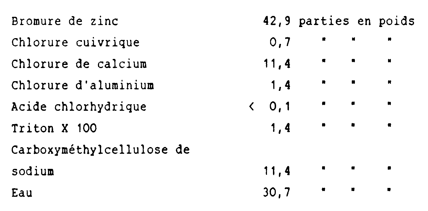
Lors du séchage de la composition formatrice fluide, la carboxyméthylcellulose de sodium est progressivement réticulée par le cation trivalent Al(III) et se trouve donc réticulée dans la couche de matériau électrolytique constitué. Cette couche adhère à la surface sur laquelle on la forme mais sa surface libre ne présente pas de collant de contact.The following fluid formative composition is prepared:
which corresponds to the electrolytic material whose composition in equilibrium with an atmospheric relative humidity of 50% is:
During the drying of the fluid forming composition, the sodium carboxymethylcellulose is progressively crosslinked by the trivalent cation Al (III) and is therefore crosslinked in the layer of electrolytic material formed. This layer adheres to the surface on which it is formed, but its free surface has no contact tack.
Sur deux plaques de verre recouvertes chacune d'une électrode transparente, on applique comme dans l'exemple 1 une couche du matériau électrolytique ci-dessus : chaque couche adhère à l'électrode transparente correspondante, mais ne présente pas de toucher collant sur sa face libre. On applique alors sur la face libre d'une de ces deux couches une très mince couche de la composition formatrice fluide de l'exemple 1, qu'on sèche, et on réunit les deux moitiés de la cellule dont la cohésion se maintient alors grâce au collant de contact de la dernière couche appliquée. Les propriétés de la cellule de transmission ainsi formée sont sensiblement les mêmes que celles de l'exemple 1, mais sa solidité mécanique est plus grande.On two glass plates each covered with a transparent electrode, a layer of the above electrolytic material is applied as in Example 1: each layer adheres to the corresponding transparent electrode, but does not have a sticky feel on its face free. A very thin layer of the fluid formative composition of Example 1 is then applied to the free face of one of these two layers, which is dried, and the two halves of the cell are combined, the cohesion of which is then maintained by with the contact adhesive of the last layer applied. The properties of the transmission cell thus formed are substantially the same as those of Example 1, but its mechanical strength is greater.
On modifie les compositions formatrices fluides et des matériaux électrolytiques, en partant de ceux décrits dans les exemples 1 et 2, et ceci de la manière suivante :
- a) On substitue aux mélanges de sels utilisés dans les exemples 1
et 2, les mélanges suivants, exprimés en poids relatifs de leurs constituants :
- b) On substitue aux résines polymères filmogènes hydrosolubles utilisées dans les exemples 1
et 2 les résines suivantes :
variante 3.2.1 Alcool polyvinylique ("Poval 224" de Kuraray) variante 3.2.2 Polyvinylpyrrolidone ("K 90" de GAF Corporation) - c) On modifie le rapport (poids de mélange de sels hydrosolubles /(poids de résine polymère) utilisé
d'environ 5 dans les exemples 1et 2 pour l'amener aux valeurs 50 et à 0,5.
- a) The following mixtures, expressed in relative weights of their constituents, are substituted for the salt mixtures used in Examples 1 and 2:
- b) The water-soluble film-forming polymer resins used in Examples 1 and 2 are substituted for the following resins:
variant 3.2.1 Polyvinyl alcohol ("Poval 224" from Kuraray) variant 3.2.2 Polyvinylpyrrolidone ("K 90" from GAF Corporation) - c) The ratio (weight of mixture of water-soluble salts / (weight of polymer resin) used by approximately 5 in Examples 1 and 2 is modified to bring it to the
values 50 and to 0.5.
Les substitutions et modifications ainsi mentionnées peuvent être combinées entre elles, c'est-à-dire que les variantes décrites peuvent être combinées.The substitutions and modifications thus mentioned can be combined with each other, that is to say that the variants described can be combined.
On réalise avec chacune des combinaisons réalisées des cellules à transmission variable de la lumière de la même manière que dans les exemples 1 et 2 précédents.Cells with variable light transmission are produced with each of the combinations made in the same manner as in Examples 1 and 2 above.
On prépare la composition formatrice fluide suivante :

correspondant au matériau électrolytique dont la composition en équilibre avec une humidité relative atmosphérique de 50% est :


On applique à l'aide d'un barreau à fil hélicoïdal des couches successives, suivies de séchages, de la composition formatrice fluide sur l'électrode transparente 2d'une plaque de verre "NESA" 15 jusqu'à obtention d'une couche du matériau électrolytique 3 correspondant d'une épaisseur totale d'une centaine de micromètres recouvrant la totalité de l'électrode transparente à l'exception d'une bande périphérique 16 ; cette couche est blanche et opaque.The following fluid formative composition is prepared:
corresponding to the electrolytic material whose composition in equilibrium with an atmospheric relative humidity of 50% is:
Successive layers, followed by drying, are applied with a helical wire bar, of the fluid forming composition to the
On découpe un disque de 6mm de diamètre dans les contre-électrodes 4 en forme de feuille mince et flexible suivantes :
- variante 4.1 Contre-électrodes en matériau homogène :
- sous-variante 4.1.1 :
- Feuille souple de graphite pur "Grafoil" de Union Carbide,
- sous-variante 4.1.2 :
- Feuille souple de graphite pur "Papyex" du Carbone-Lorraine,
- variante 4.2 Contre-électrodes en matériau composite :
- sous-variante 4.2.1 :
- Feuille de matière plastique chargée de carbone particulaire "Condulon" de Pervel Industries,
- variante 4.3 Contre-électrodes composites avec substrat conducteur :
- sous-variante 4.3.1 :
- Feuille de graphite "Papyex" recouverte d'une couche d'encre à base de graphite pour sérigraphie "Electrodag 423 SS" de Acheson,
- sous-variante 4.3.2 :
- Feuille de graphite "Papyex" recouverte d'une couche de pâte à base de graphite pour sérigraphie "TU20S" de Asahi Chemical,
- sous-variante 4.3.3 :
- Feuille de graphyte "Papyex" recouverte d'une couche de pâte à base de cuivre pour sérigraphie "ACP-020J" de Asahi Chemical,
- sous-variante 4.3.4 :
- Feuille de graphite "Papyex" recouverte d'une couche de vernis conducteur à base de nickel "Condulon 245" de Pervel Industries.
- variante 4.4 Contre-électrodes composites avec substrat isolant :
sous-variantes 4.4.1, 4.4.2, 4.4.3, et 4.4.4 respectivement identiques aux sous-variantes 4.3.1, 4.3.2, 4.3.3. et 4.3.4, sauf que la feuille flexible de graphite "Papyex" est remplacée par une feuille de non-tissé "Paratherm" de polypropylène de 30 micromètres d'épaisseur.
- variant 4.1 Counter electrodes of homogeneous material:
- Sub-variant 4.1.1:
- Flexible sheet of pure graphite "Grafoil" from Union Carbide,
- Sub-variant 4.1.2:
- Flexible sheet of pure graphite "Papyex" from Carbone-Lorraine,
- variant 4.2 Counter electrodes made of composite material:
- sub-variant 4.2.1:
- Plastic sheet loaded with particulate carbon "Condulon" from Pervel Industries,
- variant 4.3 Composite counter-electrodes with conductive substrate:
- sub-variant 4.3.1:
- Graphite sheet "Papyex" covered with a layer of graphite-based ink for screen printing "Electrodag 423 SS" from Acheson,
- sub-variant 4.3.2:
- "Papyex" graphite sheet covered with a layer of graphite paste for "TU20S" screen printing from Asahi Chemical,
- sub-variant 4.3.3:
- Graphyte sheet "Papyex" covered with a layer of copper-based paste for screen printing "ACP-020J" from Asahi Chemical,
- sub-variant 4.3.4:
- "Papyex" graphite sheet covered with a layer of conductive varnish based on nickel "Condulon 245" from Pervel Industries.
- variant 4.4 Composite counter electrodes with insulating substrate:
sub-variants 4.4.1, 4.4.2, 4.4.3, and 4.4.4 respectively identical to sub-variants 4.3.1, 4.3.2, 4.3.3. and 4.3.4, except that the flexible "Papyex" graphite sheet is replaced by a 30 micrometer thick polypropylene "Paratherm" non-woven sheet.
On dépose au verso de chacun des disques de contre-électrode, à l'opposé du matériau électrolytique une couche 17 de laque d'argent "200" de Demetron. Ces disques 4, 17 sont alors appliqués (avec un intervalle entre eux) sur la couche de matériau électrolytique 3. Enfin, on relie le verso de chaque disque 4, 17 à un bord 18 de la plaque de verre 15 à l'aide d'un ruban de cuivre 19 autocollant "EZ" de Bishop reposant sur un ruban de polyester 20 autocollant qui l'isole de la couche de matériau électrolytique 3 et de l'électrode transparente 2; ce ruban de cuivre 19, qu'on peut connecter facilement à partir du bord 18 de la plaque à une source extérieure de tension, est solidarisé électriquement avec la contre-électrode 4 à l'aide d'une goutte 21 de laque d'argent "200". Enfin, on applique sur la périphérie de l'électrode transparente un cordon périphérique de laque d'argent 22 qui permet de connecter l'électrode transparente 2 à la source extérieure de tension. Ni les contre-électrodes ni les connexions ne sont visibles ou perceptibles à travers la couche blanche opaque de matériau électrolytique. (figures 11 et 12).Is deposited on the back of each of the counter-electrode discs, opposite the electrolytic material a
Les disques 4, 17 ainsi appliqués présentent une certaine adhérence à la couche de matériau électrolytique 3, mais cette adhérence est variable d'un disque à l'autre et irrégulière d'un point à un autre d'un même disque (ce qui se traduit en fonctionnement par des hétérogénéités des densité optique). On exerce alors une pression sur chaque disque pour obtenir et maintenir un contact électrique satisfaisant.The
On applique alors une différence de potentiel de 1,5 Volt entre chaque contre-électrode en forme de disque 4, 17 et l'électrode transparente 2, cette dernière étant polarisée négativement par rapport à la contre-électrode 4 : on observe par réflexion un noircissement de chaque cellule 1 selon une aire exactement délimitée par la projection du disque 4, 17 constituant la contre-électrode. La densité optique est uniforme à l'intérieur de chaque aire et on peut la faire varier selon une échelle continue de gris en modulant la durée selon laquelle on fait passer le courant électrique. En appliquant une différence de potentiel de sens opposé également de 1,5 volt, on efface la densité optique créée et on restitue l'aspect blanc initial. On observe qu'on peut prolonger l'application de la tension d'effacement au-delà de l'effacement total sans inconvénient visible.A potential difference of 1.5 volts is then applied between each disc-shaped
La densité obtenue pour une même durée d'application de la tension d'écriture varie selon la contre-électrode, ce qui indique des différences probables d'impédance.The density obtained for the same duration of application of the write voltage varies according to the counter-electrode, which indicates probable differences in impedance.
On constate que toutes les cellules à l'exception de celles formées avec les contre-électrodes des sous-variantes 4.3.3, 4.3.4, 4.4.3 et 4.4.4 présentent un seuil d'écriture d'environ 1,25 Volts, c'est-à-dire qu'on n'observe aucun noircissement avec une tension inférieure. En revanche, les cellules formées avec les quatre contre-électrodes précitées n'ont pas de seuil.It is noted that all the cells except those formed with the counter-electrodes of the sub-variants 4.3.3, 4.3.4, 4.4.3 and 4.4.4 have a write threshold of approximately 1.25 Volts , that is to say that no blackening is observed with a lower voltage. On the other hand, the cells formed with the aforementioned four counter-electrodes have no threshold.
On répète les essais de l'exemple 4, mais en appliquant sur le recto (c'est-à-dire sur la face destinée à être en contact avec le matériau électrolytique) de chaque contre-électrode, avant découpe des disques, une couche d'une dizaine de micromètres du matériau électrolytique de l'exemple 1, selon la procédure de cet exemple 1.The tests of Example 4 are repeated, but by applying on the front (that is to say on the face intended to be in contact with the electrolytic material) of each counter-electrode, before cutting the discs, a layer about ten micrometers of the electrolytic material of example 1, according to the procedure of this example 1.
On applique alors les disques ainsi enduits sur la couche de matériau électrolytique de l'exemple 4 recouvrant l'électrode transparente sur son substrat de verre : cette fois-ci, les disques restent collés et la cohésion des cellules se maintient sans qu'il soit nécessaire d'appliquer une pression ; de même, sans pression extérieure appliquée, le fonctionnement de chaque cellule est uniforme.The discs thus coated are then applied to the layer of electrolytic material of Example 4 covering the transparent electrode on its glass substrate: this time, the discs remain glued and the cohesion of the cells is maintained without it being necessary to apply pressure; similarly, without external pressure applied, the operation of each cell is uniform.
On répète les essais de l'exemple 5 avec les différences suivantes :
- 1) on n'applique aucune couche de matériau électrolytique sur l'électrode transparente 2 fixée sur son substrat de verre 15 :
- 2) on applique sur le recto de chaque contre-
électrode 4 une couche du matériau électrolytique 3 de l'exemple 4 d'une épaisseur d'environ cent micromètres (selon la procédure d'application décrite dans l'exemple 4) ; - 3) on découpe dans les feuilles composites (contre-électrode - matériau électrolytique) ainsi réalisées des disques
composites 23 qu'on applique chacun sur l'électrode transparente 2 : ici, à la différence de ce qu'on observait dans l'exemple 4, et probablement grâce à l'uni de la surface de l'électrode transparente 2 opposée à la surface généralement irrégulière des feuilles de matériau de contre-électrode, l'adhérence est uniforme et satisfaisante, malgré le collant de surface plus faible de ce matériau que celui du matériau électrolytique de l'exemple 1 ; les cellules individuelles ne nécessitent pas l'application d'une pression pour maintenir leur cohésion structurelle ni pour assurer de bons contacts électriques. (figure 13).
- 1) no layer of electrolytic material is applied to the
transparent electrode 2 fixed on its glass substrate 15: - 2) a layer of the
electrolytic material 3 of Example 4 is applied to the front of each counter-electrode 4 with a thickness of approximately one hundred micrometers (according to the application procedure described in Example 4); - 3)
composite discs 23 are cut from the composite sheets (counter electrode - electrolytic material) thus produced, which are each applied to the transparent electrode 2: here, unlike what was observed in Example 4 , and probably thanks to the uniformity of the surface of thetransparent electrode 2 opposite the generally irregular surface of the sheets of counter-electrode material, the adhesion is uniform and satisfactory, in spite of the lower surface tackiness of this material than that of the electrolytic material of Example 1; the individual cells do not require the application of pressure to maintain their structural cohesion or to ensure good electrical contacts. (figure 13).
Le fonctionnement de chaque cellule est comparable à celui des cellules de l'exemple 5 ; la densité optique est uniforme à l'intérieur du disque composite.The operation of each cell is comparable to that of the cells of Example 5; the optical density is uniform inside the composite disc.
On applique une couche du matériau électrolytique 3 de l'exemple 4 sur une électrode transparente 2 portée par un substrat de verre 24. Sur cette couche 3, on dépose par sérigraphie des portions de couche en forme de carrés 25 de 3,5mm de côté de l'encre à base de graphite "Electrodag 423 SS". Sur ces carrés 25, après traitement thermique, on dépose également par sérigraphie des portions de couche en forme de carrés 26 de 2,5mm de côté d'encre à base d'argent "429 SS" de Acheson pour sérigraphie. On applique enfin toujours par sérigraphie une couche du vernis isolant 27 "432 SS" de Acheson pour sérigraphie recouvrant la totalité de la surface de la plaque à l'exception des carrés d'encre argentée ainsi que d'une bande 28 à la périphérie de l'électrode transparente 2.A layer of the
On dépose par projection au pistolet à travers un masque des cordons 29 de laque d'argent "200" connectant et reliant chaque carré d'encre à l'argent 26 à un bord 29 de la plaque de verre 24 à partir duquel il est plus aisé d'effectuer une liaison électrique avec une alimentation extérieure ; on dépose en même temps un cordon périphérique 30 de laque d'argent permettant également de connecter l'électrode transparente à l'alimentation extérieure. (figures 14 et 15).
L'aspect et les caractéristiques de chaque cellule sont semblables à ceux des exemples 4 et 5. En particulier, la densification est uniforme à l'intérieur d'une aire exactement délimitée par la projection orthogonale du carré 25 d'encre graphitée.The appearance and characteristics of each cell are similar to those of Examples 4 and 5. In particular, the densification is uniform within an area exactly delimited by the orthogonal projection of the square of graphitized ink.
On procède comme dans l'exemple 7 sauf que l'on dépose sur l'électrode transparente, au lieu d'une couche continue du matériau électrolytique considéré des portions de couche de ce matériau en forme de carrés de 3,7mm de côté par sérigraphie, la composition formatrice fluide de l'exemple 4 ayant été ramenée par évaporation d'eau à la viscosité convenable pour cette application. En outre, au lieu du vernis isolant transparent de l'exemple 7, on applique selon la même géométrie, en ménageant les mêmes ouvertures, une couche de quelques centaines de micromètres d'élastomère silicone blanc "Rhodorsil CAF 730" de Rhône-Poulenc qui vulcanise par séjour à l'air en quelques heures. L'aspect obtenu est le même que celui des cellules de l'exemple 7 avec une légère différence de teinte entre le blanc des carrés de matériau électrolytique et celui de l'élastomère silicone blanc, différence qui n'existe pas dans les dispositifs de l'exemple 7. Le noircissement s'effectue selon une aire qui est la projection orthogonale des carrés d'encre graphitée (et non pas l'aire des portions de matériau électrolytique).The procedure is as in Example 7 except that, on the transparent electrode, instead of a continuous layer of the electrolytic material considered, portions of the layer of this material in the form of squares of 3.7 mm sides are screen printed. , the fluid forming composition of Example 4 having been brought back by evaporation of water to the viscosity suitable for this application. In addition, instead of the transparent insulating varnish of Example 7, a layer of a few hundred micrometers of Rhône-Poulenc white silicone elastomer "Rhodorsil CAF 730" is applied using the same geometry, leaving the same openings. vulcanizes by staying in the air in a few hours. The appearance obtained is the same as that of the cells of Example 7 with a slight difference in hue between the white of the squares of material. electrolytic and that of the white silicone elastomer, difference which does not exist in the devices of example 7. The blackening is carried out according to an area which is the orthogonal projection of the squares of graphitized ink (and not the area of the portions of electrolytic material).
Sur une feuille souple de polyester de 50 micromètres d'épaisseur, on applique successivement avec séchages et/ou traitements thermiques intermédiaires :
- 1) Des portions de couche d'encre à l'argent pour sérigraphie en forme de carrés de 2,5mm de côté prolongés par un cordon continu jusqu'à un bord de la feuille ;
- 2) une couche de vernis isolant avec des ouvertures de 2,5mm de côté correspondant aux carrés précédents ;
- 3) des portions de couche d'encre graphitée pour sérigraphie en forme de carrés de 3,5mm de large centrés sur les carrés d'encre à l'argent;
- 4) une couche du matériau électrolytique de l'exemple 4.
- 1) Portions of silver ink for screen printing in the form of 2.5 mm square squares extended by a continuous cord to an edge of the sheet;
- 2) a layer of insulating varnish with 2.5 mm side openings corresponding to the previous squares;
- 3) portions of a graphite ink layer for screen printing in the form of 3.5 mm wide squares centered on the squares of silver ink;
- 4) a layer of the electrolytic material of example 4.
On applique en la déroulant la feuille composite flexible ainsi obtenue sur une plaque de verre comportant une électrode transparente (verre "NESA") munie d'une bande périphérique assurant le contact sur l'électrode transparente. La feuille composite déborde de la plaque de verre de façon à permettre l'accès aux extrémités des cordons d'encre à l'argent.The flexible composite sheet thus obtained is applied by unrolling it on a glass plate comprising a transparent electrode ("NESA" glass) provided with a peripheral strip ensuring contact with the transparent electrode. The composite sheet extends beyond the glass plate to allow access to the ends of the silver ink strings.
La feuille composite adhère à la plaque de verre "NESA" grâce au collant de surface du matériau électrolytique et la cohésion structurelle du panneau d'affichage ainsi réalisé se trouve assurée sans autre moyen.The composite sheet adheres to the "NESA" glass plate thanks to the surface tack of the electrolytic material and the structural cohesion of the display panel thus produced is ensured without other means.
Chaque cellule est individuellement adressable en appliquant une tension entre l'électrode transparente et chaque bande d'encre à l'argent reliant chaque contre-électrode. Le noircissement de chaque point-image paraît exactement délimité par la projection orthogonale de l'aire du carré d'encre graphitée.Each cell is individually addressable by applying a voltage between the transparent electrode and each strip of silver ink connecting each counter electrode. The darkening of each point-image seems exactly delimited by the orthogonal projection of the area of the graphitized ink square.
Selon une variante de réalisation du présent dispositif, la feuille plastique servant de substrat primaire est une feuille enduite d'une couche anti-adhésive présentant une très faible adhérence aux couches qu'on dépose sur elle. Après achèvement du panneau, cette feuille est retirée et n'a donc servi que d'intermédiaire commode de réalisation du panneau d'affichage.According to an alternative embodiment of the present device, the plastic sheet serving as primary substrate is a sheet coated with a non-stick layer having very poor adhesion to the layers which are deposited on it. After completion of the panel, this sheet is removed and has therefore only served as a convenient intermediary for producing the display panel.
Sur une feuille souple de polyester de 50 microns d'épaisseur, on applique successivement avec séchages et/ou traitements thermiques intermédiaires :
- 1) Des portions de couche d'encre à l'argent pour sérigraphie en forme de bandes parallèles de 0,3mm de large ;
- 2) des bandes de vernis isolant pour sérigraphie remplissant les intervalles entre les bandes d'encre à l'argent précédentes ;
- 3) des portions de couche d'encre graphitée en forme de bandes parallèles de 0,4mm de large centrées sur les bandes d'encre à l'argent ;
- 4) Des portions de couche du matériau électrolytique de l'exemple 4 en forme de bandes de 0,45mm de large centrées sur les bandes précédentes.
- 1) Portions of silver screen printing ink in the form of 0.3 mm wide parallel strips;
- 2) strips of insulating varnish for screen printing filling the gaps between the previous silver ink strips;
- 3) portions of the graphitized ink layer in the form of 0.4 mm wide parallel strips centered on the silver ink strips;
- 4) Layer portions of the electrolytic material of Example 4 in the form of strips 0.45 mm wide centered on the preceding strips.
On applique en la déroulant la feuille composite ainsi obtenue sur une plaque de verre revêtue d'une couche transparente conductrice de dioxyde d'étain configurée en bandes parallèles indépendantes de 3,5mm de côté séparées par un intervalle de 0,1mm de diamètre, l'orientation de la feuille composite par rapport à la plaque étant telle que les bandes d'électrode transparente soient perpendiculaires aux bandes de la feuille composite. La feuille composite déborde de la plaque de verre de façon à ce que les extrémités de ses bandes soient accessibles pour connexion à l'électronique d'adressage et de commande.The composite sheet thus obtained is applied by unrolling it on a glass plate coated with a transparent conductive layer of tin dioxide configured in independent parallel strips of 3.5 mm side separated by an interval of 0.1 mm in diameter, l orientation of the composite sheet relative to the plate being such that the transparent electrode strips are perpendicular to the strips of the composite sheet. The composite sheet projects beyond the glass plate so that the ends of its strips are accessible for connection to the addressing and ordered.
La feuille composite adhère à la plaque de verre revêtue de ses électrodes transparentes grâce au collant de surface du matériau électrolytique et la cohésion structurelle du panneau d'affichage ainsi réalisé se trouve assurée sans autre moyen.The composite sheet adheres to the glass plate coated with its transparent electrodes by virtue of the surface adhesive of the electrolytic material and the structural cohesion of the display panel thus produced is ensured without other means.
Les colonnes constituées par les bandes d'électrodes conductrices sont reliées par leurs extrémités à une électronique d'adressage et de commande à laquelle sont également reliées les extrémités des bandes d'encre à l'argent constituant les conducteurs de lignes du panneau.The columns formed by the strips of conductive electrodes are connected at their ends to addressing and control electronics to which are also connected the ends of the silver ink strips constituting the line conductors of the panel.
L'écriture matricielle du panneau peut s'effectuer ligne après ligne : une tension d'écriture est appliquée entre d'une part toutes les colonnes sélectionnées et d'autre part une ligne donnée : on noircit ainsi les points-image sélectionnés de la ligne considérée sans noircir les points-image non sélectionnés de la même ligne ni ceux des lignes précédentes et suivantes, ceci résultant de la valeur élevée du seuil de tension par rapport à la tension d'écriture ainsi que de caractéristiques favorables de la mémoire.The matrix writing of the panel can be done line after line: a writing voltage is applied between on the one hand all the selected columns and on the other hand a given line: we thus blacken the selected image points of the line considered without blackening the unselected image points of the same line or those of the preceding and following lines, this resulting from the high value of the voltage threshold relative to the writing voltage as well as from favorable characteristics of the memory.
Selon une variante de réalisation du présent dispositif, la feuille plastique servant de substrat primaire est une feuille enduite d'une couche de résine hydrofugeante siliconée présentant une faible adhérence aux couches qu'on dépose sur elle. Après achèvement du panneau, cette feuille est retirée et n'a donc servi que d'intermédiaire commode de réalisation du panneau d'affichage.According to an alternative embodiment of the present device, the plastic sheet serving as the primary substrate is a sheet coated with a layer of silicone water-repellent resin having poor adhesion to the layers which are deposited on it. After completion of the panel, this sheet is removed and has therefore only served as a convenient intermediary for producing the display panel.
Cet exemple concerne un panneau d'affichage à adressage direct destiné à un caractère alphanumérique à sept segments (figures 16, 17, 18, 19, 20).This example concerns a direct addressing display panel intended for an alphanumeric character with seven segments (FIGS. 16, 17, 18, 19, 20).
Un tel panneau permet de réaliser l'un des dix chiffres 0 à 9 respectivement, à partir de sept segments linéaires juxtaposés 31A, 31B, 31C, 31D, 31E, 31F et 31G, cette disposition étant connue en soi et comportant quatre segments répartis deux à deux bout à bout sur deux lignes longitudinales parallèles et trois segments transversaux respectivement supérieur 31E, inférieur 31F et médian 31G.Such a panel makes it possible to produce one of the ten digits 0 to 9 respectively, from seven juxtaposed
Ce panneau comporte de la partie frontale tournée vers le lecteur à la partie arrière, une plaque de verre 32 et sur la face arrière de celle-ci, une couche ou un revêtement mince et transparent conducteur electronique, par exemple d'oxyde d'étain formant l'électrode de travail 2. Dans une première variante (figures 18 et 19), des portions de couche de matériau électrolytique 3 tel que celui précédemment décrit et des portions de couche de la contre-électrode 4 également telle que celle précédemment décrite sont superposées, en regard l'une de l'autre, en étant agencées pour constituer les segments 31A à 31G mentionnés précédemment. Selon la structure générale déjà décrite précédemment, la couche de matériau électrolytique 3 est en contact avec l'électrode de travail 2, tandis qu'une contre-électrode 4 est en contact avec sur le matériau 3. Les différents segments 31A à 31G sont séparés les uns des autres par des espaces 33 pouvant être très faibles par exemple, un écartement de l'ordre de 0,5mm pour un caractère de l'ordre de 12cm de haut. Dans une seconde variante (figure 11c), la couche de matériau électrolytique 3 occupe la presque totalité de la surface de la couche transparente conductrice électrode de travail 2 à l'exception d'une bande périphérique 34.This panel comprises from the front part facing the reader at the rear part, a
Dans ces deux formes de réalisation décrites, sont prévus des conducteur de l'électricité filiformes formant amenées de courant électrique à l'électrode transparente 2 constitué avec une pâte ou encre conductrice ou équivalent décrite précédemment. Plus précisément, et dans le cas d'un caractère alphanumérique à sept segments 31A à 31G, il est prévu trois conducteurs filiformes ou longilignes 35A, 35B, 35C entourant les segments 31A à 31G, respectivement à l'extérieur et à l'intérieur, ainsi qu'il est représenté sur la figure 16 à laquelle on se réfère expressément. Cette disposition permet une amenée et une distribution de l'énergie électrique aussi régulière et satisfaisante que possible pour les différents segments. Le mode de réalisation du matériau connecteur électrique formant les conducteurs filiformes ou longilignes 35A, 35B, 35C, de même que leur association à la plaque 32 du côté de la couche et formant électrode de travail 2 ont été déjà décrits précédemment et ne sont pas décrits de nouveau ici.In these two embodiments described, there are provided filiform electricity conductors forming electric current leads to the
Par ailleurs, sont prévus des conducteurs de l'électricité en forme de bandes 36 chacune propre et appliquée au contact d'un segment 31A à 31G et de forme semblable mais de dimensions inférieures à celles du segment 31A à 31G concerné constitué avec une pâte ou encre conductrice ou équivalent également décrite précédemment formant amenée de courant aux contre-électrodes 4 des segments 31A à 31G. En effet, en général, dans ce genre d'application, la surface disponible pour l'application de ce matériau conducteur sur la contre-électrode 4 est plus important que celle possible sur l'électrode 2, et, de surcroît, les bandes 35 ne sont pas visibles depuis la face frontale du panneau. Dans cette application, qui fonctionne par réflexion, et dans la structure indiquée, il est nécessaire de prévoir un matériau de masquage 37 constituant un fond pour le panneau, ce matériau de masquage 37 étant agencé en couche et laissant toutefois apparaître, naturellement, les conducteurs filiformes ou longilignes 35A, 35B, 35C et les portions de couche de matériau 3. Un tel matériau de masquage 37 a également été décrit précédemment et n'est pas de nouveau décrit ici. Ce matériau de masquage recouvre les chants des portions de couches de matériau électrolytique 3 et des contre-électrodes 4 et partiellement le verso de ces dernières contribuant à la cohésion du panneau et assurant une isolation des cellules ainsi constituées.Furthermore, electrical conductors are provided in the form of
Les moyens de connexion électrique et de support mécanique complémentaire du panneau sont constituées par une plaque arrière 38, parallèle à la plaque de verre 32 et pouvant être associée à celle-ci, notamment par ses bords, par un joint d'association 39, notamment en élastomère silicone, un tel joint 39 ayant la capacité d'absorber des différences de mouvement entre la plaque arrière 38 et la plaque de verre 32.The means of electrical connection and of complementary mechanical support of the panel are constituted by a
Dans une forme de réalisation illustrée plus spécialement par la figure 18, la plaque 38 est une plaque de circuit imprimé et comporte, au droit d'une bande, 36, un trou 40 dans lequel peut être engagé un cavalier 41 électriquement conducteur qui, par son extrémité interne 42 vient au contact électronique de la bande 36 et, par son extrémité externe rabattue 43, vient sur la face extérieure 44 de la plaque 38 être appliqué et au contact d'un conducteur 45 plat de la plaque 38 sur lequel il peut être maintenu et associé électriquement au moyen d'une encre ou pâte conductrice ou équivalente 46. Les différents conducteurs 45 (en l'occurence sept) correspondant aux différents segments 31A à 31G sont associés électriquement à un connecteur embrochable 47 se trouvant sur un bord de la plaque 38. Ce connecteur embrochable 47 comporte huit positions dont sept 48 correspondent aux sept contre électrodes 4 des segments 31A à 31G via les conducteurs 45 et les cavaliers 41 et un, 49 correspond à l'électrode 2 via d'autres cavaliers 50, traversant d'autres trous 51 au droit des conducteurs filiformes ou longilignes 35A, 35B, 35C, les cavaliers 50 étant agencé sur un conducteur 52 de la plaque 38, ce conducteur 52 étant constitué par la face arrière électriquement conductrice de cette plaque à l'exception des conducteurs 45, les différents conducteurs 45 et 52 étant isolés les uns des autres.In an embodiment illustrated more particularly in FIG. 18, the
Selon une autre variante (figure 19), des manchons de connexion électrique 53 prolongeant les conducteurs 45 et 52 sont prévus dans les trous 40 et 51 et on coule dans chacun de ces manchons une goutte de matériau de connexion électrique 54 telle qu'une encre ou pâte conductrice ou équivalent qui vient au contact des bandes 36 ou des conducteurs 35A, 35B, 35Cet y assure une "soudure" électrique.According to another variant (FIG. 19),
Les deux variantes de réalisation objet des figures 18 et 19 correspondent à la troisième variante, objet de la figure 8C précédemment décrite.The two embodiments which are the subject of FIGS. 18 and 19 correspond to the third variant, which is the object of FIG. 8C previously described.
Le panneau peut également faire l'objet d'une réalisation conforme à la première variante de la figure 8A également décrite (figure 20). A cet effet, le matériau électrolytique forme une couche 3 continue et non plus une couche fractionnée en segments. Cela permet également que la couche de matériau 3 forme un fond contrastant pour les segments d'image 31A à 31G. Les contre-électrodes 4 sont réalisées comme précédemment, de même que les amenées de courant et connexions électriques en ce qui concerne les contre-électrodes 4. Dans ce cas, le contour des contre-électrodes 4 définit la forme des segments d'image 31A à 31G. Les amenées de courant de l'électrode de travail 2 sont réalisées soit au moyen d'un conducteur filiforme entourant la plaque 32 sur sa face interne, à la périphérie, c'est-à-dire, sur la couche constituant l'électrode 2 et à l'extérieur de la couche de matériau électrolyte 3 c'est-à-dire dans la bande périphérique 34, soit par points, ces points étant répartis de façon appropriée pour assurer une distribution convenable de l'énergie électrique.The panel can also be made in accordance with the first variant of Figure 8A also described (Figure 20). For this purpose, the electrolytic material forms a
Selon un détail de réalisation objet de la figure 21, on peut associer aux amenées de courant réalisées en un premier matériau 55 électroniquement conducteur tel qu'une encre ou pâte conductrice ou équivalent précédemment décrit une bande ou fil 56 en un second matériau plus conducteur, par exemple, une bande ou un fil de cuivre, ce second matériau 56 faiblement résistif étant en liaison électrique avec les amenées de courant précédentes 55par recouvrement ou enrobage partiel au moyen d'un complément 57 du premier matériau.According to a detail of embodiment which is the object of FIG. 21, it is possible to associate with the current leads produced in a first electronically
Sur la figure 22 est réprésentée une autre variante de réalisation d'un panneau d'affichage comportant plusieurs - en particulier trois en l'occurrence - caractères 58A, 58B, 58C à sept segments chacun, chacun comme décrit précédemment. Ces trois caractères 58A, 58B, 58C permettent alors d'afficher un nombre compris entre 000 et 999. Les trois caractères 58A, 58B, 58C sont juxtaposés et le panneau est partagé en trois zones respectivement 59A, 59B, 59C sur chacune desquelles se trouve un des trois caractères respectivement 58A, 58B, 58C. A cet effet, l'électrode de travail 2 et, en particulier, la couche conductrice sur la plaque de verre 32 est elle-même distribuée en trois portions électriquement distinctes et juxtaposées, séparées l'une de l'autre par un espace minimal tel que 60 qui peut atteindre une dizaine de microns de largeur. La couche de matériau électrolytique 3, de couleur blanche, est distribuée en portions de couches ayant la forme, la dimension et l'emplacement des segments constituant chaque caractère 58A, 58B, 58C. L'espace 61 extérieur aux segments est recouvert d'une couche de matériau masquant et contrastant blanc.FIG. 22 shows another alternative embodiment of a display panel comprising several - in particular three in this case -
Dans une première forme de mise en oeuvre, les contre-électrodes 4 des segments identiques des trois caractères 58A, 58B, 58C peuvent être connectés entre eux, en parallèle. De plus, dans cette même première forme de mise en oeuvre, chacune des portions de couche, en ce qui concerne l'électrode de travail 2, est alimentée séparément. Le panneau ainsi constitué comporte un connecteur embrochable 62 à dix sorties, à savoir sept sorties 63 pour les sept contre-électrodes 4 de segments homologues des trois caractères 58A, 58B, 58C et trois sorties 64pour les trois portions de l'électrode de travail 2 transparente. Le nombre de connexions électriques est limité tout en permettant de commander l'écriture des différents caractères en temps partagé. La réalisation particulière de chaque caractère, peut être conforme à ce qui a été décrit précédemment dans le cas d'un caractère unique de l'exemple 11. Selon une variante de réalisation, (figure 22) l'amenée de courant électrique relative à l'électrode 2 peut être faite sous forme d'une pluralité de points, tels que 65, au lieu de conducteurs filiformes et longilignes tels que ceux précédemment décrits dans l'exemple 11. Ces points sont distribués autour des caractères 58A, 58B, 58C de manière à assurer une répartition de l'énergie électrique aussi convenable que possible. Egalement, en variante, le matériau masquant est noir au lieu d'être blanc, et les points 65, sont noirs. En variante (figure 23), la distribution électrique concernant l'électrode 2 peut être réalisée non par des amenées de courant ponctuelles telles que 65, ainsi qu'il vient d'être décrit, mais par des bandes longitudinales 66, ménagées sur les bords du panneau à un endroit où il n'y a pas de matériau électrolytique 3. Cette variante autorise les différentes combinaisons de configurations conjuguées précédemment décrites en relation avec les schémas des figures 8. En particulier, la couche de matériau électrolytique 3 peut être continue, ce qui permet d'éviter la présence d'un matériau de masquage.In a first embodiment, the
Une second forme de mise en oeuvre (non représentée) diffère essentiellement de celle qui vient d'être décrite par le fait que d'une part l'électrode de travail transparente conductrice est commune à tous les caractères, c'est-à-dire commune à toutes les cellules élémentaires du dispositif; et que, d'autre part, l'électrode de travail et chaque contre-électrode individuellement sont reliées électriquement soit à une ou plusieurs zones de connexion situées au verso du panneau constitué par le substrat de verre et les composants du dispositif mentionnés précédemment, soit à un connecteur solidaire d'une plaque de circuit imprimé appliqué au verso du panneau, soit au moyen de contacts situés au droit des électrodes et portés par le bâti du dispositif auquel est intégré le panneau d'affichage. Dans le cas considéré qui comporte trois caractères à sept segments chacun, la liaison électrique avec l'électronique d'alimentation et de commande extérieure est réalisée au moyen de vingt-deux conducteurs indépendants. Dans le cas de l'emploi d'une plaque de circuit imprimé, la liaison électrique entre chaque amenée de courant et le conducteur correspondant de la plaque peut être réalisé ainsi qu'il est décrit dans l'exemple 11.A second embodiment (not shown) differs essentially from that which has just been described by the fact that on the one hand the transparent conductive working electrode is common to all the characters, that is to say common to all the elementary cells of the device; and that, on the other hand, the working electrode and each counter-electrode individually are electrically connected either to one or more connection zones located on the back of the panel formed by the glass substrate and the components of the device mentioned above, or to a connector secured to a printed circuit board applied to the back of the panel, either by means of contacts located to the right of the electrodes and carried by the frame of the device in which the display panel is integrated. In the case under consideration which comprises three characters with seven segments each, the electrical connection with the power supply and external control electronics is achieved by means of twenty-two independent conductors. In the case of the use of a printed circuit board, the electrical connection between each current supply and the corresponding conductor of the board can be produced as described in Example 11.
On décrit maintenant un autre exemple de réalisation concernant un panneau d'affichage matriciel (figures 24 à 27) permettant d'afficher par exemple des caractères alphanumériques. Un tel panneau comporte des points-image agencés aux intersections de plusieurs lignes 67 et plusieurs colonnes 68, juxtaposés les uns aux autres, identiques les uns aux autres, en constituant ainsi une matrice permettant, selon la commande qui est faite, une écriture d'un caractère alphanumérique, d'un signe, d'une figure souhaitée. Dans cet exemple, le panneau comporte une plaque de verre 69 frontale sur la face arrière duquel sont réalisées des bandes 70 transparentes et électroniquement conductrices, constituant des d'électrodes 2 communes chacune à toutes les cellules d'une même colonne 68. Les bandes 70 peuvent être très proches les unes des autres, séparées par des intervalles juste nécessaires pour éviter le contact électrique entre elles selon la technique utilisée. Dans cet exemple, les portions de couche de matériau électrolytique 3 et les contre-électrodes 4 sont superposées, de même forme et de mêmes dimensions, et localisées à l'endroit de chaque noeud de ligne 67 et colonne 68, de manière à déterminer chacun des points-image, dont la plus grande dimension, dans le sens des lignes est légèrement inférieure à la largeur des bandes 70, en étant situés en totalité au droit et à l'intérieur d'une de ces bandes 70.We will now describe another exemplary embodiment concerning a matrix display panel (FIGS. 24 to 27) making it possible to display, for example, alphanumeric characters. Such a panel comprises image points arranged at the intersections of
Au verso de chaque contre-électrode 4, une amenée de courant est réalisée au moyen d'un matériau de connexion déjà décrit pour de telles amenées.On the back of each counter-electrode 4, a current supply is produced by means of a connection material already described for such supplies.
Sur chacune des lignes, un conducteur électrique 71 tel qu'un ruban de cuivre, relie électriquement entre elles les différentes contre-électrodes 4 d'une même ligne 67 sur leur verso. L'association et le contact entre ce conducteur 71 et les amenées de courant des contre-électrodes 4 est réalisé au moyen du complément 72 de même matériau recouvrant ou enrobant que l'amenée elle-même. Un isolant électrique sépare le conducteur 71 des autres composants conducteurs du panneau dans les intervalles situés entre les points-image.On each of the lines, an
Dans la forme de réalisation dans laquelle les points-image sont de petites dimensions par exemple celles des points-image d'un écran d'ordinateur, il est en général suffisant de prévoir des amenées de courant pour les électrodes de travail 2 seulement aux extrémités des bandes 70.In the embodiment in which the image points are small, for example those of the image points of a computer screen, it is generally sufficient to provide current leads for the working
Dans la forme de réalisation représentée dans laquelle les points-image ont une aire unitaire importante la conductivité généralement modeste des électrodes de travail 2 peut entraîner une alimentation électrique non uniforme des cellules élémentaires, il est prévu un mode de distribution du courant électrique sur une bande 72 comprenant des amenées de courant 73 agencées en tronçons de lignes filiformes parallèlement aux lignes 67 et placées entre les points-image tout en étant isolées du matériau électrolytique et des contre-électrodes 4. En variante, les amenées peuvent être distribuées en points. De plus, les amenées de courant 473d'une même bande 70 sont connectées entre elles à l'aide d'un conducteur-collecteur 74, par exemple un ruban de cuivre ou une bande de laque d'argent agencé selon la colonne 68 correspondante et relié aux amenées 73 de cette colonne correspondante, par un complément 75 de matériau d'amenée réalisant l'enrobage partiel ou le recouvrement.In the embodiment shown in which the image points have a large unit area, the generally modest conductivity of the working
Un isolant électrique sépare le conducteur-collecteur 74 de tous les autres composants conducteurs du panneau.An electrical insulator separates the conductor-
De plus, est prévu un matériau de masquage 76 en couche recouvrant la face arrière de la plaque de verre 69 à l'exception des zones ou se trouve le matériau électrolytique, ainsi que les zones réservées aux amenées de courant aux électrodes. Cette disposition est telle que les conducteurs-collecteurs 74 sont masqués par le matériau de masquage 76 et peuvent, sans préjudice, être placés à tout endroit souhaite, pourvu que le conducteur-conducteur 74 d'une colonne 68 ne soit pas au contact électrique des amenées de courant 73 de la colonne 68 voisine. A cet effet et à défaut d'isolant électrique intermédiaire, la longueur (dans le sens des lignes 67) des amenées 73 est suffisante sans être excessive pour ne pas interférer avec le conducteur-collectuer 74 de la colonne 68 voisine. Dans ce mode de réalisation, les conducteurs électriques 71 croisent les conducteurs-collecteurs 74, sans contact électrique par exemple à l'aide d'un isolant intercalaire. Dans le cas les conducteurs-collecteurs 74 sont des bandes de cuivre suffisamment rigides, il n'y a pas contact électrique avec les conducteurs 71 entre eux, étant donné qu'ils se trouvent les uns et les autres dans deux plans distincts séparés l'un de l'autre par un intervalle égal à l'épaisseur de la cellule, l'air formant isolant. En effet, les conducteurs-collecteurs 74 sont placés au voisinage du plan de la face arrière de la plaque 69, alors que les conducteurs électriques 71 sont placés dans un autre plan écarté correspondant à la surface libre arrière des contre-électrodes 4.In addition, a masking
Un tel panneau peut être également associé, vers l'arrière, à une plaque de circuit imprimé 77 assurant les contacts électriques avec les conducteurs 71 de chaque ligne 67 et les conducteurs-collecteurs 74 de chaque colonne 68. Dans le cas de figure représenté, dans lequel le panneau comporte cinq lignes 67 et cinq colonnes 68, la plaque de circuit imprimé 77 comporte dix conducteurs 78 isolés les uns des autres pouvant être reliés à un connecteur latéral embrochable 79 à dix positions comme décrit dans l'exemple 11. Dès lors, en appliquant la différence de tension électrique requise entre un conducteur électrique 71 et un conducteur-collecteur 74 via le connecteur embrochable 79 et les conducteurs 78, on permet l'écriture du point-image correspondant à l'intersection des ligne et colonne 67 et 68, correspondant à ces conducteurs 71 et 74. De plus, il est possible d'appliquer la tension électrique d'écriture entre un unique conducteur électrique 46 et plusieurs conducteurs-collecteurs 74 ou, inversement, entre un unique conducteur-collecteur 74 et plusieurs conducteurs 71.Such a panel can also be associated, towards the rear, with a printed
Ce mode de réalisation peut faire lui-même l'objet de très nombreuses variantes. En ce qui concerne tout d'abord la taille même des points-images, ceux-ci peuvent varier du très petit (tels que le point-image d'un écran d'ordinateur) au très grand (par exemple, des points-image ayant un encombrement de l'ordre du centimètre ou même plus) notamment dans le cas d'un panneau d'affichage public. Les variantes concernent ensuite la conjugaison des configurations constitutives du panneau. Dans la forme de réalisation décrite, les électrodes de travail en forme de bande 70 sont communes à chaque colonne 68 et séparées entre les colonnes 68. Les portions de couche de matériau électrolytique 3 et les contre-électrodes 4 sont distinctes et propres à chaque cellule élementaire. Mais, dans d'autres variantes de réalisation, on peut concevoir d'autres combinaisons de conjugaison de configuration, ainsi qu'il a déjà été décrit en référence aux figures 8. Les variantes peuvent concerner également les connexions électriques internes au dispositif d'affichage, notamment conformément à ce qui a été mentionné dans les exemples précédents. Enfin, les variantes peuvent concerner le procédé de fabrication même d'un tel panneau ainsi qu'il a été décrit précédemment.This embodiment can itself be the subject of numerous variations. First of all with regard to the size of the image points themselves, these can vary from very small (such as the image point of a computer screen) to very large (for example, image points having a footprint of the order of a centimeter or even more) especially in the case of a public display panel. The variants then relate to the conjugation of the constitutive configurations of the panel. In the embodiment described, the strip-shaped working
Claims (32)
- A Light-modulating cell (1), enabling writing at least one image point or image segment (5), maintaining such a written image point or image segment (5), reversibly, erasure of such an image point or image segment (5), and maintaining the erased state of the image point or image segment (5), the writing of an image point or image segment (5) being defined as a local increase in optical density, and the erasure of an image point or image segment (5) being defined as a reduction or disappearance of the increase in the optical density obtained during writing, said cell comprising, at least, in combination:1) a first electrode (2) called working electrode, transparent or substantially transparent and electronically conducting;2) a second electrode (4) called counter-electrode, spaced transversely from the working electrode (2) and electronically conducting;3) at least one layer or portion of layer of material (3) having ionic electroconductivity, in contact with and interposed between the two electrodes (2, 4) in the region of an image point or image segment (5);4) electrical connection zones for conducting electrical current to the working electrode (2)and counter-electrode (4), capable in particular of enabling on the one hand, application to the working electrode (2) of an electrical voltage which is negative with respect to that of the counter-electrode (4) and, on the other hand, allowing flow between the electrodes (2, 4) of a current whose direction is opposite to that of the electrical current resulting from application of the previous voltage, characterized in that said material1) comprises a homogeneous mixture of solid consistency, comprising the following constituents :a) a hydrosoluble salt or a hydrosoluble mixture of salts of at least one metal which can be cathodically deposited from an aqueous solution of one of its simple or complex ions;b) at least one initially hydrosoluble film-forming polymer resin;c) water; andd) an auxiliary redox couple, said mixture is able to reversibly (1) develop metal or metal alloy deposits by cathodic reduction of at least one depositable metal ion present within the mixture, and (2) by anodic oxidation, dissolve the deposits and reincorporate into their original state the metal ion or ions produced by this oxidation; the constituents (a), (b), (c) and (d) being selected so as to allow plastic or viscoelastic deformability;2) can be formed in a continuous layer of a thickness, in particular, of between a few microns and a few tens of microns.
- The light-modulating cell according to Claim 1, characterized in that the counter-electrode (4) is transparent or substantially transparent such that the cell can function in particular by transmission.
- The light-modulating cell according to Claim 1, characterized in that the counter-electrode (4) is opaque, the cell functioning by reflection.
- The light-modulating cell according to Claim 3, characterized in that it further comprises a reflecting and/or masking and/or diffusing element located between the working electrode (2) and the counter-electrode (4).
- The light-modulating cell according to any one of Claims 1 to 4, characterized in that a working electrode (2) and/or a counter-electrode (4) includes a self-supporting structure or is supported by a self-supporting substrate.
- The light-modulating cell according to Claim 5, characterized in that the substrate is transparent or substantially transparent when the electrode which is associated with it is itself transparent or substantially transparent.
- The light-modulating cell according to any one of Claims 1 to 6, characterized in that said layer of material (3) has adhesive properties, in particular, a tacky touch or a sticky contact.
- The light-modulating cell according to any one of Claims 1 to 7, characterized in that it comprises at least two of said layers of material (3) which are separate, combined and, in particular, superimposed and/or juxtaposed.
- The light-modulating cell according to Claim 8, characterized in that said two materials (3) constituting two layers are different.
- The light-modulating cell according to Claim 8, characterized in that each layer contains a different percentage of the total constituents of a same material (3), the layers together containing them all.
- The light-modulating cell according to any one of claims 1 to 10, characterized in that the electrodes (2, 4) have an overall curvature or localized reliefs, the latter being applied to the cell itself.
- The light-modulating cell according to any one of claims 1 to 11, characterized in that one of said layers of material (3) is continuous.
- The light-modulating cell according to any one of Claims 1 to 11, characterized in that one of said layers of at least one material (3) is of juxtaposed granules or particles held by themselves or by a binder.
- The light-modulating cell according to any one of claims 1 to 13, characterized in that it further comprises specific supplementary means for maintaining its cohesion, the permanence of the electrical contacts; and/or specific supplementary means of isolation and protection of its constituent elements from the ambient atmosphere; and/or a specific spacer.
- The light-modulating cell according to any one of claims 1 to 14, characterized in that, in combination, said layer of material (3) is substantially rigid and that the cell (1) has no specific spacer between the two electrodes (2, 4).
- The light-modulating cell according to any one of Claims 1 to 15, characterized in that, in combination, on the one hand, said layer of material (3) has a tacky touch or a sticky contact and, on the other hand, the cell has no specific supplementary means for maintaining its cohesion.
- The light-modulating cell according to any one of Claims 1 to 16, characterized in that, in combination, on the one hand, said layer of material (3) has a permanent ionic conductivity, including when in contact with external ambient atmosphere and on the other hand, the cell has no specific means ensuring its leak-tightness.
- The light-modulating cell according to any one of Claims 1 to 17, characterized in that an image point or image segment (5) is determined in shape, size and position exclusively by intersection of orthogonal projections on a screen surface, of the areas of the working electrode (2), counter-electrode (4) and said layer of material (3).
- The light-modulating cell according to Claim 18, characterized in that the area of the working electrode (2), counter-electrode (4), layer of material (3) is determined in shape, size and position by intersection of orthogonal projections, on a screen surface of the areas of the other two components.
- The light-modulating cell according to Claim 18, characterized in that the areas of two components, working electrode (2), counter-electrode (4), layer of material (3) are identical and superimposed and their common orthogonal projection on the third component is included in the area of the latter.
- A process for manufacturing a light-modulating cell (1), according to any one of Claims 1 to 20, characterized in that it comprises at least the steps consisting in :1) First fabricating a fluid formative composition comprising at least the constituents of the material (3) as mentioned in Claim 1 and additional water in quantities such that this fluid formative composition has the desired viscosity for its application in layer;2) Forming one layer of a fluid formative composition on one of the two electrodes;3) Giving said layer its solid consistency; and4) Applying the other electrode to the free face of said layer.
- The process for manufacturing a light-modulating cell (1) according to Claim 21, characterized in that there is firstly formed a layer on at least one electrode and that this layer is then treated, in particular by evaporation, heat treatment, cross-linking or vulcanization to obtain its solid consistency.
- The process for manufacturing a light-modulating cell (1) according to Claim 21, characterized in that the layer is firstly treated in particular by evaporation or heat treatment to obtain its solid consistency and that the layer is then formed on at least one electrode.
- The process for manufacturing a light-modulating cell (1) according to any one of Claims 21 to 23, characterized in that it comprises a step consisting in forming at least one layer of material (3) on one of the two electrodes (2, 4) and another subsequent step consisting in applying this layer, by its free face, to the other electrode.
- The process for manufacturing a light-modulating cell (1) according to any one of Claims 21 to 23, characterized in that it comprises a step consisting in forming at least a first layer of material on one of the two electrodes, another step consisting in forming at least a second layer on the other electrode and another subsequent step consisting in joining the first and second layers by their free faces.
- The process for manufacturing a light-modulating cell (1) according to any one of Claims 21 to 25, characterized in that said layer is formed in one pass in the case of simple layer or in several successive or non-successive passes in the case of composite layer of formative compositions which may be identical or different.
- The process for manufacturing a light-modulating cell (1) according to any one of claims 21 to 26, characterized in that in order to form said layer of material (3) adhering to an electrode, a surface or contact adhesive properties are given to the layer of material (3).
- The process for manufacturing a light-modulating cell (1) according to any one of Claims 21 to 27, characterized in that in order to form said layer of material (3) on an electrode, the material (3) and the electrode are either directly applied in contact with each other, or the material (3) is first applied to a temporary, intermediate substrate, particularly one having a non-adhering surface, and the layer of material (3) is then transferred from the substrate to the electrode concerned.
- The process for manufacturing a light-modulating cell (1) according to any one of Claims 21 to 28, characterized in that the formative composition is applied in one or more layers of total thickness preferably between a few microns and a few hundred microns.
- The process for manufacturing a light-modulating cell (1) according to any one of Claims 21 to 29, characterized in that the formative composition comprises at least the constituents of said material (3) and additional water, and possibly agents for maintaining the stability and/or conservation and/or facilitating the application in layers of the formative composition.
- The process for manufacturing a light-modulating cell (1) according to any one of Claims 21 to 30, characterized in that the viscosity of the fluid formative composition is adjusted to a suitable value for a particular method of formation and/or application in layers by evaporation of part of its water or by addition of additional water.
- Light-modulating cell (1) according to any one of Claims 1 to 20, characterized in that the electrical connection zones are distributed in such a way as to obtain a current density which is as uniform as possible inside the image point or image segment (5).
Priority Applications (1)
| Application Number | Priority Date | Filing Date | Title |
|---|---|---|---|
| AT88401914T ATE99429T1 (en) | 1987-07-24 | 1988-07-22 | CELL FOR LIGHT MODULATION. |
Applications Claiming Priority (2)
| Application Number | Priority Date | Filing Date | Title |
|---|---|---|---|
| FR8710562 | 1987-07-24 | ||
| FR8710562A FR2618566B1 (en) | 1987-07-24 | 1987-07-24 | LIGHT MODULATION CELL |
Publications (2)
| Publication Number | Publication Date |
|---|---|
| EP0300916A1 EP0300916A1 (en) | 1989-01-25 |
| EP0300916B1 true EP0300916B1 (en) | 1993-12-29 |
Family
ID=9353555
Family Applications (1)
| Application Number | Title | Priority Date | Filing Date |
|---|---|---|---|
| EP88401914A Expired - Lifetime EP0300916B1 (en) | 1987-07-24 | 1988-07-22 | Cell for the modulation of light |
Country Status (10)
| Country | Link |
|---|---|
| US (1) | US5078480A (en) |
| EP (1) | EP0300916B1 (en) |
| JP (1) | JPS6444424A (en) |
| AT (1) | ATE99429T1 (en) |
| AU (1) | AU2127388A (en) |
| DE (1) | DE3886609T2 (en) |
| DK (1) | DK133389A (en) |
| ES (1) | ES2049755T3 (en) |
| FR (1) | FR2618566B1 (en) |
| WO (1) | WO1989001177A1 (en) |
Families Citing this family (67)
| Publication number | Priority date | Publication date | Assignee | Title |
|---|---|---|---|---|
| US5672440A (en) * | 1991-01-31 | 1997-09-30 | Eveready Battery Company | Cell tester device employing a cathodically depositable metal ion electrolyte solution |
| US5413739A (en) * | 1992-12-22 | 1995-05-09 | Coleman; James P. | Electrochromic materials and displays |
| US5754329A (en) * | 1992-12-22 | 1998-05-19 | Monsanto Company | Electrochromic display laminates |
| US5910854A (en) | 1993-02-26 | 1999-06-08 | Donnelly Corporation | Electrochromic polymeric solid films, manufacturing electrochromic devices using such solid films, and processes for making such solid films and devices |
| US5668663A (en) | 1994-05-05 | 1997-09-16 | Donnelly Corporation | Electrochromic mirrors and devices |
| US5679283A (en) * | 1994-07-22 | 1997-10-21 | Gentex Corporation | Electrochromic layer and devices comprising same |
| US5523776A (en) * | 1995-01-10 | 1996-06-04 | International Business Machines Corporation | Photovoltaic array for computer display |
| US5891511A (en) * | 1995-12-26 | 1999-04-06 | Monsanto Company | Addition of color to electrochromic displays |
| US5876633A (en) * | 1995-12-26 | 1999-03-02 | Monsanto Company | Electrochromic metal oxides |
| US5876634A (en) * | 1995-12-26 | 1999-03-02 | Monsanto Company | Electrochromic tin oxide |
| US5928572A (en) * | 1996-03-15 | 1999-07-27 | Gentex Corporation | Electrochromic layer and devices comprising same |
| US6178034B1 (en) | 1996-04-10 | 2001-01-23 | Donnelly Corporation | Electrochromic devices |
| US5825526A (en) * | 1996-04-24 | 1998-10-20 | Minnesota Mining And Manufacturing Company | Tape for use in manufacturing electrochromic devices |
| US5847860A (en) * | 1996-07-17 | 1998-12-08 | International Business Machines Corporation | High density electrochromic display |
| US6369792B1 (en) * | 1996-09-19 | 2002-04-09 | Lextron Systems, Inc. | Low power high resolution electrochemical display |
| US5774255A (en) * | 1996-09-23 | 1998-06-30 | Mcdonnell Douglas Corporation | Adaptive infrared modulator |
| AU4669897A (en) | 1996-10-01 | 1998-04-24 | National Label Company | Apparatus and method for assembling electrochromic cells |
| US5877888A (en) * | 1997-06-10 | 1999-03-02 | Monsanto Company | Single and double sided electrochromic displays |
| US6172613B1 (en) * | 1998-02-18 | 2001-01-09 | Donnelly Corporation | Rearview mirror assembly incorporating vehicle information display |
| US8294975B2 (en) | 1997-08-25 | 2012-10-23 | Donnelly Corporation | Automotive rearview mirror assembly |
| US6124886A (en) | 1997-08-25 | 2000-09-26 | Donnelly Corporation | Modular rearview mirror assembly |
| US6326613B1 (en) | 1998-01-07 | 2001-12-04 | Donnelly Corporation | Vehicle interior mirror assembly adapted for containing a rain sensor |
| US8288711B2 (en) | 1998-01-07 | 2012-10-16 | Donnelly Corporation | Interior rearview mirror system with forwardly-viewing camera and a control |
| US6445287B1 (en) | 2000-02-28 | 2002-09-03 | Donnelly Corporation | Tire inflation assistance monitoring system |
| US6477464B2 (en) | 2000-03-09 | 2002-11-05 | Donnelly Corporation | Complete mirror-based global-positioning system (GPS) navigation solution |
| US6329925B1 (en) | 1999-11-24 | 2001-12-11 | Donnelly Corporation | Rearview mirror assembly with added feature modular display |
| US6693517B2 (en) | 2000-04-21 | 2004-02-17 | Donnelly Corporation | Vehicle mirror assembly communicating wirelessly with vehicle accessories and occupants |
| DE19920942A1 (en) * | 1999-05-07 | 2000-11-16 | Daddy Technology Gmbh | Large display device |
| WO2001064481A2 (en) | 2000-03-02 | 2001-09-07 | Donnelly Corporation | Video mirror systems incorporating an accessory module |
| US7370983B2 (en) | 2000-03-02 | 2008-05-13 | Donnelly Corporation | Interior mirror assembly with display |
| US7855755B2 (en) | 2005-11-01 | 2010-12-21 | Donnelly Corporation | Interior rearview mirror assembly with display |
| US7167796B2 (en) | 2000-03-09 | 2007-01-23 | Donnelly Corporation | Vehicle navigation system for use with a telematics system |
| US6690500B2 (en) * | 2000-06-30 | 2004-02-10 | Pioneer Corporation | Aberration correction apparatus and method |
| US7255451B2 (en) * | 2002-09-20 | 2007-08-14 | Donnelly Corporation | Electro-optic mirror cell |
| US7581859B2 (en) | 2005-09-14 | 2009-09-01 | Donnelly Corp. | Display device for exterior rearview mirror |
| DE60220379T2 (en) | 2001-01-23 | 2008-01-24 | Donnelly Corp., Holland | IMPROVED VEHICLE LIGHTING SYSTEM |
| US6918674B2 (en) | 2002-05-03 | 2005-07-19 | Donnelly Corporation | Vehicle rearview mirror system |
| EP1514246A4 (en) | 2002-06-06 | 2008-04-16 | Donnelly Corp | Interior rearview mirror system with compass |
| US7329013B2 (en) | 2002-06-06 | 2008-02-12 | Donnelly Corporation | Interior rearview mirror system with compass |
| US7310177B2 (en) * | 2002-09-20 | 2007-12-18 | Donnelly Corporation | Electro-optic reflective element assembly |
| WO2004026633A2 (en) | 2002-09-20 | 2004-04-01 | Donnelly Corporation | Mirror reflective element assembly |
| US7360932B2 (en) * | 2004-06-01 | 2008-04-22 | Donnelly Corporation | Mirror assembly for vehicle |
| WO2004103772A2 (en) | 2003-05-19 | 2004-12-02 | Donnelly Corporation | Mirror assembly for vehicle |
| US7184190B2 (en) * | 2002-09-20 | 2007-02-27 | Donnelly Corporation | Electro-optic reflective element assembly |
| AU2003287535A1 (en) * | 2002-11-05 | 2004-06-07 | Donnelly Corporation | Electro-optic reflective element assembly |
| US7420756B2 (en) * | 2003-05-20 | 2008-09-02 | Donnelly Corporation | Mirror reflective element |
| US7446924B2 (en) | 2003-10-02 | 2008-11-04 | Donnelly Corporation | Mirror reflective element assembly including electronic component |
| US7308341B2 (en) * | 2003-10-14 | 2007-12-11 | Donnelly Corporation | Vehicle communication system |
| US7400435B2 (en) * | 2005-01-19 | 2008-07-15 | Donnelly Corporation | Mirror assembly with heater element |
| US7626749B2 (en) | 2005-05-16 | 2009-12-01 | Donnelly Corporation | Vehicle mirror assembly with indicia at reflective element |
| US11242009B2 (en) | 2005-07-06 | 2022-02-08 | Donnelly Corporation | Vehicular exterior mirror system with blind spot indicator |
| US11498487B2 (en) | 2005-07-06 | 2022-11-15 | Magna Mirrors Of America, Inc. | Vehicular exterior mirror system with blind spot indicator |
| US8058977B2 (en) | 2006-10-24 | 2011-11-15 | Donnelly Corporation | Exterior mirror having a display that can be viewed by a host driver or drivers of other vehicles |
| US7944371B2 (en) | 2007-11-05 | 2011-05-17 | Magna Mirrors Of America, Inc. | Exterior mirror with indicator |
| US11890991B2 (en) | 2006-10-24 | 2024-02-06 | Magna Mirrors Of America, Inc. | Vehicular exterior rearview mirror assembly with blind spot indicator element |
| US7748856B2 (en) * | 2007-05-23 | 2010-07-06 | Donnelly Corporation | Exterior mirror element with integral wide angle portion |
| US8154418B2 (en) | 2008-03-31 | 2012-04-10 | Magna Mirrors Of America, Inc. | Interior rearview mirror system |
| US7813023B2 (en) * | 2008-06-09 | 2010-10-12 | Magna Mirrors Of America, Inc. | Electro-optic mirror |
| US9205780B2 (en) | 2010-02-04 | 2015-12-08 | Magna Mirrors Of America, Inc. | Electro-optic rearview mirror assembly for vehicle |
| US9481304B2 (en) | 2010-05-24 | 2016-11-01 | Magna Mirrors Of America, Inc. | Automotive exterior mirror heater control |
| US8988755B2 (en) | 2011-05-13 | 2015-03-24 | Magna Mirrors Of America, Inc. | Mirror reflective element |
| US8736940B2 (en) | 2011-09-30 | 2014-05-27 | Magna Mirrors Of America, Inc. | Exterior mirror with integral spotter mirror and method of making same |
| US8801245B2 (en) | 2011-11-14 | 2014-08-12 | Magna Mirrors Of America, Inc. | Illumination module for vehicle |
| US9216691B2 (en) | 2013-02-25 | 2015-12-22 | Magna Mirrors Of America, Inc. | Exterior mirror with spotter mirror |
| US11235699B2 (en) | 2014-02-07 | 2022-02-01 | Magna Mirrors Of America, Inc. | Illumination module for vehicle |
| US9761144B2 (en) | 2014-09-11 | 2017-09-12 | Magna Mirrors Of America, Inc. | Exterior mirror with blind zone indicator |
| US9659498B2 (en) | 2015-09-28 | 2017-05-23 | Magna Mirrors Of America, Inc. | Exterior mirror assembly with blind zone indicator |
Citations (2)
| Publication number | Priority date | Publication date | Assignee | Title |
|---|---|---|---|---|
| FR2260167A1 (en) * | 1974-01-31 | 1975-08-29 | Ind Horlogere Management | |
| US4285575A (en) * | 1978-02-15 | 1981-08-25 | Canon Kabushiki Kaisha | Image display device |
Family Cites Families (31)
| Publication number | Priority date | Publication date | Assignee | Title |
|---|---|---|---|---|
| GB909342A (en) * | 1958-02-03 | 1962-10-31 | Eastman Kodak Co | Improvements in or relating to a device for controlling light transmission or reflection |
| JPS5132197A (en) * | 1974-09-12 | 1976-03-18 | Canon Kk | |
| US4188095A (en) * | 1975-07-29 | 1980-02-12 | Citizen Watch Co., Ltd. | Liquid type display cells and method of manufacturing the same |
| CH594263A5 (en) * | 1975-11-29 | 1977-12-30 | Ebauches Sa | |
| BE849076A (en) * | 1975-12-08 | 1977-06-03 | ELECTROCHROME COMPOSITIONS | |
| US4127853A (en) * | 1976-04-12 | 1978-11-28 | Timex Corporation | Electrochromic display adapted for multiplexing |
| US4116535A (en) * | 1976-05-10 | 1978-09-26 | U.S. Philips Corporation | Picture display cell with memory effect |
| FR2352361A1 (en) * | 1976-05-19 | 1977-12-16 | Commissariat Energie Atomique | ELECTROLYTIC DISPLAY DEVICE WITH ABSORBENT DEPOSIT |
| GB1586104A (en) * | 1976-07-12 | 1981-03-18 | Matsushita Electric Ind Co Ltd | Electrochromic display apparatus and method |
| US4116545A (en) * | 1976-10-27 | 1978-09-26 | American Cyanamid Company | Polymeric electrolyte for electrochromic display devices |
| JPS5461576U (en) * | 1977-10-11 | 1979-04-28 | ||
| US4246579A (en) * | 1978-03-01 | 1981-01-20 | Timex Corporation | Electrochromic display switching and holding arrangement |
| FR2434449A1 (en) * | 1978-06-19 | 1980-03-21 | Commissariat Energie Atomique | METHOD FOR CONTROLLING AN ELECTROLYTIC DISPLAY CELL USING A LEAKAGE CURRENT FOR ERASING AND CIRCUIT IMPLEMENTING THIS METHOD |
| FR2468179A1 (en) * | 1979-10-17 | 1981-04-30 | Commissariat Energie Atomique | ELECTROLYTIC DISPLAY CELL COMPRISING AN ELECTROLYTE WITH TWO METAL SALTS |
| FR2504290B1 (en) * | 1981-04-21 | 1986-08-01 | Hopkinson Associates Inc | ELECTROSENSITIVE METHOD AND MEDIUMS FOR RECORDING SIGNALS AND IMAGES |
| JPS58207027A (en) * | 1982-05-27 | 1983-12-02 | Nec Corp | All solid-state type electrochromic display |
| DE3211638A1 (en) * | 1982-03-30 | 1983-10-13 | Robert Bosch Gmbh, 7000 Stuttgart | ELECTROCHROME DISPLAY DEVICE WITH REFLECTIVE BACKGROUND |
| US4538158A (en) * | 1982-04-21 | 1985-08-27 | Bernard Warszawski | Electrosensitive media and recording process |
| US4596722A (en) * | 1982-04-21 | 1986-06-24 | Hopkinson Associates Inc. | Electrosensitive media and recording process |
| JPS5950486A (en) * | 1982-09-17 | 1984-03-23 | 株式会社東芝 | Electric coloring display element |
| JPS5979226A (en) * | 1982-10-29 | 1984-05-08 | Asahi Glass Co Ltd | Dimming body |
| JPS59195629A (en) * | 1983-04-21 | 1984-11-06 | Toppan Printing Co Ltd | Electrochromic display body |
| JPS6098480A (en) * | 1983-11-02 | 1985-06-01 | 株式会社ニコン | Transmission type electrochromic disply unit |
| US4573768A (en) * | 1983-12-05 | 1986-03-04 | The Signal Companies, Inc. | Electrochromic devices |
| US4571029A (en) * | 1983-12-29 | 1986-02-18 | The United States Of America As Represented By The United States Department Of Energy | Electro-optical switching and memory display device |
| US4652090A (en) * | 1984-04-20 | 1987-03-24 | Nippon Kogaku K. K. | Dispersed iridium based complementary electrochromic device |
| JPS614165A (en) * | 1984-06-15 | 1986-01-10 | Sumitomo Chem Co Ltd | Reversible electrochemical cell with conjugated system polymer as electrode active material |
| JPS61119527A (en) * | 1984-11-14 | 1986-06-06 | Sumitomo Metal Ind Ltd | Carrying/stocking method of steel pipe |
| JPS61138238A (en) * | 1984-12-11 | 1986-06-25 | Tokuyama Soda Co Ltd | Electrochromic display element |
| US4801195A (en) * | 1985-01-29 | 1989-01-31 | Nissan Motor Co., Ltd. | Variable light transmittance glass board functional as electrochromic cell |
| JPS61223724A (en) * | 1985-03-28 | 1986-10-04 | Alps Electric Co Ltd | Electrochromic display element |
-
1987
- 1987-07-24 FR FR8710562A patent/FR2618566B1/en not_active Expired - Lifetime
-
1988
- 1988-07-22 DE DE3886609T patent/DE3886609T2/en not_active Expired - Fee Related
- 1988-07-22 AU AU21273/88A patent/AU2127388A/en not_active Abandoned
- 1988-07-22 EP EP88401914A patent/EP0300916B1/en not_active Expired - Lifetime
- 1988-07-22 ES ES88401914T patent/ES2049755T3/en not_active Expired - Lifetime
- 1988-07-22 WO PCT/FR1988/000380 patent/WO1989001177A1/en unknown
- 1988-07-22 AT AT88401914T patent/ATE99429T1/en not_active IP Right Cessation
- 1988-07-25 JP JP63183748A patent/JPS6444424A/en active Pending
-
1989
- 1989-03-17 DK DK133389A patent/DK133389A/en not_active Application Discontinuation
-
1990
- 1990-01-10 US US07/463,788 patent/US5078480A/en not_active Expired - Fee Related
Patent Citations (2)
| Publication number | Priority date | Publication date | Assignee | Title |
|---|---|---|---|---|
| FR2260167A1 (en) * | 1974-01-31 | 1975-08-29 | Ind Horlogere Management | |
| US4285575A (en) * | 1978-02-15 | 1981-08-25 | Canon Kabushiki Kaisha | Image display device |
Also Published As
| Publication number | Publication date |
|---|---|
| FR2618566A1 (en) | 1989-01-27 |
| JPS6444424A (en) | 1989-02-16 |
| EP0300916A1 (en) | 1989-01-25 |
| DK133389D0 (en) | 1989-03-17 |
| AU2127388A (en) | 1989-03-01 |
| WO1989001177A1 (en) | 1989-02-09 |
| ES2049755T3 (en) | 1994-05-01 |
| DE3886609T2 (en) | 1994-07-21 |
| ATE99429T1 (en) | 1994-01-15 |
| US5078480A (en) | 1992-01-07 |
| DE3886609D1 (en) | 1994-02-10 |
| FR2618566B1 (en) | 1992-04-17 |
| DK133389A (en) | 1989-05-10 |
Similar Documents
| Publication | Publication Date | Title |
|---|---|---|
| EP0300916B1 (en) | Cell for the modulation of light | |
| EP0300915B1 (en) | Material for the modulation of light and methods of manufacture | |
| EP0300919B1 (en) | Method for manufacturing a device for modulating light | |
| EP0300918B1 (en) | Process for manufacturing a device for modulating light | |
| EP0300914B1 (en) | Process for modulating light | |
| JP2002258327A (en) | Electrochromic display element and electrodeposition type display element | |
| EP0698226A1 (en) | Complementary surface confined polymer electrochromic materials, systems, and methods of fabrication therefor | |
| CA2117802A1 (en) | Electrochromic light modulation devices, in particular screens and displays | |
| EP0300917B1 (en) | Devices for modulating light | |
| Howard et al. | Optical properties of reversible electrodeposition electrochromic materials | |
| FR2669121A1 (en) | IMPROVED MATERIAL AND CELL FOR LIGHT MODULATION AND METHOD FOR MANUFACTURING THE SAME | |
| US5071233A (en) | Electrochromic device with oxymethylene-polyoxyethylene electrolyte | |
| EP0592328A1 (en) | Materials, cells, devices, method of manufacturing a colour electrochromic display | |
| JP4700386B2 (en) | Display element and manufacturing method thereof | |
| FR2505067A1 (en) | ELECTROLYTIC DISPLAY CELL WITH TRANSPARENT REAR BLADE |
Legal Events
| Date | Code | Title | Description |
|---|---|---|---|
| PUAI | Public reference made under article 153(3) epc to a published international application that has entered the european phase |
Free format text: ORIGINAL CODE: 0009012 |
|
| AK | Designated contracting states |
Kind code of ref document: A1 Designated state(s): AT BE CH DE ES FR GB GR IT LI LU NL SE |
|
| 17P | Request for examination filed |
Effective date: 19890616 |
|
| 17Q | First examination report despatched |
Effective date: 19910802 |
|
| GRAA | (expected) grant |
Free format text: ORIGINAL CODE: 0009210 |
|
| AK | Designated contracting states |
Kind code of ref document: B1 Designated state(s): AT BE CH DE ES FR GB GR IT LI LU NL SE |
|
| PG25 | Lapsed in a contracting state [announced via postgrant information from national office to epo] |
Ref country code: SE Effective date: 19931229 Ref country code: GR Free format text: LAPSE BECAUSE OF FAILURE TO SUBMIT A TRANSLATION OF THE DESCRIPTION OR TO PAY THE FEE WITHIN THE PRESCRIBED TIME-LIMIT Effective date: 19931229 Ref country code: AT Effective date: 19931229 |
|
| REF | Corresponds to: |
Ref document number: 99429 Country of ref document: AT Date of ref document: 19940115 Kind code of ref document: T |
|
| REF | Corresponds to: |
Ref document number: 3886609 Country of ref document: DE Date of ref document: 19940210 |
|
| ITF | It: translation for a ep patent filed |
Owner name: BUGNION S.P.A. |
|
| GBT | Gb: translation of ep patent filed (gb section 77(6)(a)/1977) |
Effective date: 19940322 |
|
| REG | Reference to a national code |
Ref country code: ES Ref legal event code: FG2A Ref document number: 2049755 Country of ref document: ES Kind code of ref document: T3 |
|
| PGFP | Annual fee paid to national office [announced via postgrant information from national office to epo] |
Ref country code: GB Payment date: 19940722 Year of fee payment: 7 |
|
| PG25 | Lapsed in a contracting state [announced via postgrant information from national office to epo] |
Ref country code: ES Free format text: LAPSE BECAUSE OF NON-PAYMENT OF DUE FEES Effective date: 19940723 |
|
| PGFP | Annual fee paid to national office [announced via postgrant information from national office to epo] |
Ref country code: FR Payment date: 19940729 Year of fee payment: 7 |
|
| PG25 | Lapsed in a contracting state [announced via postgrant information from national office to epo] |
Ref country code: LU Free format text: LAPSE BECAUSE OF NON-PAYMENT OF DUE FEES Effective date: 19940731 Ref country code: LI Effective date: 19940731 Ref country code: CH Effective date: 19940731 Ref country code: BE Effective date: 19940731 |
|
| PLBE | No opposition filed within time limit |
Free format text: ORIGINAL CODE: 0009261 |
|
| STAA | Information on the status of an ep patent application or granted ep patent |
Free format text: STATUS: NO OPPOSITION FILED WITHIN TIME LIMIT |
|
| 26N | No opposition filed | ||
| BERE | Be: lapsed |
Owner name: ALPINE POLYVISION INC. Effective date: 19940731 |
|
| PG25 | Lapsed in a contracting state [announced via postgrant information from national office to epo] |
Ref country code: NL Effective date: 19950201 |
|
| NLV4 | Nl: lapsed or anulled due to non-payment of the annual fee | ||
| REG | Reference to a national code |
Ref country code: CH Ref legal event code: PL |
|
| PG25 | Lapsed in a contracting state [announced via postgrant information from national office to epo] |
Ref country code: GB Effective date: 19950722 |
|
| GBPC | Gb: european patent ceased through non-payment of renewal fee |
Effective date: 19950722 |
|
| PG25 | Lapsed in a contracting state [announced via postgrant information from national office to epo] |
Ref country code: FR Effective date: 19960430 |
|
| REG | Reference to a national code |
Ref country code: FR Ref legal event code: ST |
|
| REG | Reference to a national code |
Ref country code: FR Ref legal event code: ST |
|
| REG | Reference to a national code |
Ref country code: FR Ref legal event code: ST |
|
| PGFP | Annual fee paid to national office [announced via postgrant information from national office to epo] |
Ref country code: DE Payment date: 20000403 Year of fee payment: 12 |
|
| PG25 | Lapsed in a contracting state [announced via postgrant information from national office to epo] |
Ref country code: DE Free format text: LAPSE BECAUSE OF NON-PAYMENT OF DUE FEES Effective date: 20010501 |
|
| REG | Reference to a national code |
Ref country code: ES Ref legal event code: FD2A Effective date: 19950810 |
|
| PG25 | Lapsed in a contracting state [announced via postgrant information from national office to epo] |
Ref country code: IT Free format text: LAPSE BECAUSE OF NON-PAYMENT OF DUE FEES;WARNING: LAPSES OF ITALIAN PATENTS WITH EFFECTIVE DATE BEFORE 2007 MAY HAVE OCCURRED AT ANY TIME BEFORE 2007. THE CORRECT EFFECTIVE DATE MAY BE DIFFERENT FROM THE ONE RECORDED. Effective date: 20050722 |