EP0289944B1 - Caméra électronique numérique d'images fixes utilisant l'accumulation des composants des signaux de vidéo dans une mémoire - Google Patents
Caméra électronique numérique d'images fixes utilisant l'accumulation des composants des signaux de vidéo dans une mémoire Download PDFInfo
- Publication number
- EP0289944B1 EP0289944B1 EP88106858A EP88106858A EP0289944B1 EP 0289944 B1 EP0289944 B1 EP 0289944B1 EP 88106858 A EP88106858 A EP 88106858A EP 88106858 A EP88106858 A EP 88106858A EP 0289944 B1 EP0289944 B1 EP 0289944B1
- Authority
- EP
- European Patent Office
- Prior art keywords
- signals
- video signals
- signal processing
- color
- processing means
- Prior art date
- Legal status (The legal status is an assumption and is not a legal conclusion. Google has not performed a legal analysis and makes no representation as to the accuracy of the status listed.)
- Expired - Lifetime
Links
Images


Classifications
-
- H—ELECTRICITY
- H04—ELECTRIC COMMUNICATION TECHNIQUE
- H04N—PICTORIAL COMMUNICATION, e.g. TELEVISION
- H04N1/00—Scanning, transmission or reproduction of documents or the like, e.g. facsimile transmission; Details thereof
- H04N1/21—Intermediate information storage
- H04N1/2104—Intermediate information storage for one or a few pictures
- H04N1/2158—Intermediate information storage for one or a few pictures using a detachable storage unit
-
- H—ELECTRICITY
- H04—ELECTRIC COMMUNICATION TECHNIQUE
- H04N—PICTORIAL COMMUNICATION, e.g. TELEVISION
- H04N1/00—Scanning, transmission or reproduction of documents or the like, e.g. facsimile transmission; Details thereof
- H04N1/21—Intermediate information storage
- H04N1/2104—Intermediate information storage for one or a few pictures
- H04N1/2112—Intermediate information storage for one or a few pictures using still video cameras
-
- H—ELECTRICITY
- H04—ELECTRIC COMMUNICATION TECHNIQUE
- H04N—PICTORIAL COMMUNICATION, e.g. TELEVISION
- H04N1/00—Scanning, transmission or reproduction of documents or the like, e.g. facsimile transmission; Details thereof
- H04N1/46—Colour picture communication systems
- H04N1/64—Systems for the transmission or the storage of the colour picture signal; Details therefor, e.g. coding or decoding means therefor
- H04N1/646—Transmitting or storing colour television type signals, e.g. PAL, Lab; Their conversion into additive or subtractive colour signals or vice versa therefor
-
- H—ELECTRICITY
- H04—ELECTRIC COMMUNICATION TECHNIQUE
- H04N—PICTORIAL COMMUNICATION, e.g. TELEVISION
- H04N5/00—Details of television systems
- H04N5/76—Television signal recording
- H04N5/765—Interface circuits between an apparatus for recording and another apparatus
- H04N5/77—Interface circuits between an apparatus for recording and another apparatus between a recording apparatus and a television camera
- H04N5/772—Interface circuits between an apparatus for recording and another apparatus between a recording apparatus and a television camera the recording apparatus and the television camera being placed in the same enclosure
-
- H—ELECTRICITY
- H04—ELECTRIC COMMUNICATION TECHNIQUE
- H04N—PICTORIAL COMMUNICATION, e.g. TELEVISION
- H04N9/00—Details of colour television systems
- H04N9/79—Processing of colour television signals in connection with recording
- H04N9/80—Transformation of the television signal for recording, e.g. modulation, frequency changing; Inverse transformation for playback
- H04N9/81—Transformation of the television signal for recording, e.g. modulation, frequency changing; Inverse transformation for playback the individual colour picture signal components being recorded sequentially only
-
- H—ELECTRICITY
- H04—ELECTRIC COMMUNICATION TECHNIQUE
- H04N—PICTORIAL COMMUNICATION, e.g. TELEVISION
- H04N2101/00—Still video cameras
-
- H—ELECTRICITY
- H04—ELECTRIC COMMUNICATION TECHNIQUE
- H04N—PICTORIAL COMMUNICATION, e.g. TELEVISION
- H04N2201/00—Indexing scheme relating to scanning, transmission or reproduction of documents or the like, and to details thereof
- H04N2201/0077—Types of the still picture apparatus
-
- Y—GENERAL TAGGING OF NEW TECHNOLOGICAL DEVELOPMENTS; GENERAL TAGGING OF CROSS-SECTIONAL TECHNOLOGIES SPANNING OVER SEVERAL SECTIONS OF THE IPC; TECHNICAL SUBJECTS COVERED BY FORMER USPC CROSS-REFERENCE ART COLLECTIONS [XRACs] AND DIGESTS
- Y10—TECHNICAL SUBJECTS COVERED BY FORMER USPC
- Y10S—TECHNICAL SUBJECTS COVERED BY FORMER USPC CROSS-REFERENCE ART COLLECTIONS [XRACs] AND DIGESTS
- Y10S358/00—Facsimile and static presentation processing
- Y10S358/906—Hand-held camera with recorder in a single unit
Definitions
- This invention relates to an electronic still camera and more particularly to a digital electronic still camera in which video signals representative of a still image or scene are stored in the form of digital data in a memory.
- a memory is detachably connected to the main body of the camera including an imaging optical system and a solid state imaging device, and the video signals representing the still image or scene imaged by the imaging device are stored in the memory in the form of digital signals.
- the memory with the video signals stored therein is detached from the electronic still camera and loaded into a playback unit.
- the video signals read out from the memory by the playback unit are reproduced as a visual image on a screen of a video monitor.
- the solid state imaging devices mounted on the camera in general have an array of color filter segments and spectral transmittivities that are proper to the specific imaging devices.
- various combinations of pixels are employed, such as the combinations of pixels of cyan (Cy), magenta (M), yellow (Ye) and green (G); red (R), green (G) and blue (B); or cyan (Cy), white (W), yellow (Ye) and green (G).
- the pixels in a line are different in color from pixel to pixel, while in others, the pixels of the same color are arrayed in the perpendicular direction of the screen.
- color separation data concerning the pixel array and spectral properties of the solid state imaging device which is mounted on the camera are stored in the memory in the form of codes along with the video signals each time a scene is shot by the camera.
- the playback unit has a series of color separation processing programs for handling a variety of the solid state imaging devices. This is in consideration that, unless the relative disposition between the pixel array of the photosensitive cells and the filter segment array of the color filter or the phasing relation between the drive timing of the imaging device and the analog to digital converter and the timing of data writing into the memory are determined appropriately, pixel signals of the correct color cannot be reproduced upon reproducing the video signals by the playback unit.
- an occasionally suitable color separation processing program is accessed on the basis of the color separation data or information for the image at the time the video signals are read out and reproduced from the memory, and the operation of color separation is carried out in accordance with the thus selected processing program.
- the color separation processing programs need be stored in the memory of the playback unit in association with these different imaging devices.
- the memory capacity of the playback unit is necessarily increased with increase in complexity of the system, and increased costs. In view of increasing variations in the imaging devices, it would be more and more difficult to handle them properly in the playback system.
- video signals are stored in the form of component signals from the digital electronic still camera to the memory so that processing of the video signals in the playback system may be performed independently upon the difference in kinds of imaging devices.
- component signals means a concept somewhat contrary to the composite video signals and hence may be in the form of three prime color signals or of luminance and color-difference signals. Those component signals may naturally be dot or pixel sequential or line sequential signals.
- the video signals are stored in the memory in the form of the component signals that are of the standard signal format as the video signals.
- the image may be reproduced appropriately in the playback unit without the necessity of performing imaging- device-oriented signal processing operations, such as color separation.
- imaging- device-oriented signal processing operations such as color separation.
- video signal processing at the playback system is not affected by the difference in the kinds of the solid state imaging devices.
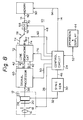
- FIG. 1 there is shown an embodiment of the digital electronic still camera comprised of a camera 10 including an imaging subsystem 12 and a memory 90 detachably connected to the camera by means of connectors 14.
- a camera 10 including an imaging subsystem 12 and a memory 90 detachably connected to the camera by means of connectors 14.
- parts or elements towards the left of the connector 14 represent those of the digital electronic still camera enclosed in a housing, not shown.
- the memory 90 is a rewritable digital storage unit loaded for example with a SRAM semiconductor memory in the form of a module such as an integrated circuit or IC card or cartridge and has a data input and output lines 92 and a control line 94 for address, read/write enable, chip select, strobe and clock signals, for example, connected by connectors 14 to the camera 10. It is noted that the connectors may 14 include power supply lines to the memory 90.
- a storage unit of two chips for 24 picture frames would be realized with the memory 90 with an SRAM with the memory capacity of 16M bits per chip.
- the imaging subsystem 12 includes parts or elements necessary for shooting a still image, such as an objective lens 16, diaphragm 18, shutter 20, an imager or image pickup device 22, light and distance measurement unit, view finder, not shown, and a drive unit or units for these elements.
- the focusing of the objective lens 16 and the control of the diaphragm 18 as well as the opening and closure of the shutter 20 may be controlled by a control circuit 24 over a control line 26.
- a solid-state image pickup device such as a CCD or MOS device, or an image pickup tube, may be advantageously employed for the image pickup device 22.
- a color filter 28 is attached to an array of photosensitive cells of the solid-state image pickup device.
- the solid-state image pickup device Responsive to clocks received from a sync generator 30 on a drive line 32, the solid-state image pickup device produces color-separated image signals at an output 34 in a dot or pixel sequential fashion.
- the color filter 28 may have any desired disposition of filter segments.
- the video signal output 34 of the image pickup device 22 is connected to an input of an analog-to-digital converter or ADC 36.
- the ADC 36 is a signal converter adapted for converting the video signals of the analog format at the input 34 into corresponding digital data of, for example, 8 bits, and supplying the digital data at the output 38 connected to an input of a signal processing circuit 40.
- the signal processing circuit 40 is a video signal processing circuit adapted for color separating video signals at the input 38 and subjecting the resulting color-separated signals to video signal processing operations such as white balance adjustment, or gradation or gamma correcting operations, prior to developing the signals at the output 42.
- the circuit 40 may additionally be adapted for forming chrominance or color-difference signals.
- the output 42 is connected to the connectors 14 of the camera.
- the control circuit 24 is responsive to command signals from an operation and display unit 44 on a signal line 52.
- the control signals from the circuit 24 are coupled through control lines 46, 26, 48 and 50 to the sync generator 30, image pickup subsystem 12, analog to digital converter 36 and to the signal processing section 40, respectively.
- the control circuit 24 also operates to monitor the state of various parts of the camera through these control lines 46, 26, 48 and 50.
- the control circuit 24 also has the function to control mainly the write function of the memory 90 and, to this end, has a control line 54 for write address, write enable, chip select and clock signals, for example, connected to the connector 14.
- the sync generator 30 is controlled through control line 46 from the control circuit 24 and issues drive signals, such as clock or address signals, necessary to drive the image pickup device 22 to cause video signals to be issued at the output 34.
- the operation and display unit 44 has a number of manually operating buttons, such as a shutter release button or those for auto/manual setting, exposure setting or white balance adjustment. With the aid of these operating buttons, the operator's commands may be entered to the camera and transmitted to the control circuit 24 over the signal line 52.
- the display unit 44 also operates to receive signals indicating the operating states of the camera from the control circuit 24 for display to the operator.
- the signal processing circuit 40 preferably includes a color separator circuit 100, a white balance adjustment circuit 102 and a gamma corrector 104.
- the color separator 100 operates to separate pixel-sequential video signals at the input 38 into color-separated component signals, such as red (R), green (G) and blue (B) signals, in accordance with pixel clocks received from the control circuit 24 over the control line 50.
- This color separation is carried out in accordance with the array of the filter segments of the color filter 28 of the image pickup device 22.
- the filter segments may be arrayed in any suitable manner.
- the color-separated component signals are introduced into a white balance adjustment circuit 102.
- the section 102 is responsive to control line 50 from the control circuit 24 to correct white balance deviation with the color temperature of the light source under which an image is shot with the image pickup device 22.
- the white balance adjusted component signals are introduced into gamma corrector 104.
- the gamma corrector 104 operates to correct the shift or deviation in gradation caused for example by non-linear characteristics of the image pickup device 22.
- the output of the gamma corrector 104 is connected to the output 42 of the signal processing circuit 40.
- FIG. 10 shows an alternative embodiment of the signal processing circuit 40.
- the signal processing circuit 40 differs from the embodiment shown in FIG. 9 in that a matrix 106 is arranged between the output 42 and the output of the gamma corrector 104 in the embodiment of FIG. 10.
- the matrix 106 operates to produce a luminance signal Y and chrominance or color-difference signals R-Y and B-Y from the component signals R, G and B obtained at the gamma corrector 104 to transmit these luminance and color-difference signals at the three outputs 42. In this manner, the luminance signal Y and color-difference signals R-Y are issued to the outputs 42 of the signal processing circuit 40.
- the signal processing circuit 40 shown in FIGS. 9 and 10 may be designed as a digital signal processing system for processing digital format color signals, or as an analog operational circuit for processing analog format color signals. Such signal processing circuit 40 may for example be implemented advantageously on an IC chip. In the embodiment shown in FIG. 1, the signal processing circuit 40 is implemented by a digital processing system.
- the memory 90 is attached to the camera by the connector 14 and then the operation and display unit 44 is manipulated to shoot or photograph an object.
- Signals representative of a frame of object image captured by the image pickup device 22 upon releasing the shutter 20 in response to an actuation of the shutter release button is developed in the form of dot- or pixel-sequential video signals at the output 34 of the image pickup device 22 timed with the clock signals supplied from the sync generator 30 on the clock line 32.
- the control circuit 24 enables the analog-to-digital converter 36 and the signal processing circuit 40 in response to sync signals produced by the sync generator 30.
- the dot-sequential video signals are converted by the analog to digital converter 36 into corresponding digital data before being fed to the signal processing circuit 40.
- the digital data are separated in the color separating circuit 100 into for example three color component signals of red (R), green (G) and blue (B), and the resulting three component signals are adjusted for white balance and gradation in the white balance adjustment circuit 102 and the gamma corrector circuit 104, respectively.
- the video signals thus modified in various manners are issued at the output 42 in the form of the color signals R, G and B or the data of the luminance signal Y and the color-difference signals R-Y and B-Y, that is, in the form of component signal data.
- the control circuit 24 also issues control signals such as write address, write enable, chip select and clock signals, on the control line 54 to the memory 90.
- control signals such as write address, write enable, chip select and clock signals, on the control line 54 to the memory 90.
- video signals supplied to the data line 92 are sequentially written into storage locations of the memory 90.
- video signal data representing a frame of image are stored in the form of component signal data in the storage area of the memory 90.
- signal processor 40 may be adapted to accomplish data compression, such as the Hadamard transform, cosine transform or orthogonal transform, and coding on the video signal data, which is in turn transferred to and stored in memory 90.
- data compression such as the Hadamard transform, cosine transform or orthogonal transform
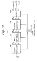
- the video signals stored in the memory 90 in the form of, for example, R, G and B component signals may be reproduced by a playback unit 120 shown for example in FIG. 11.
- the playback unit 120 has a connector 122 to which the memory 90 is detachably connected and by means of which a read-out data line 96 of the memory 90 is connected through a digital-to-analog converter or DAC 124 to a matrix 126.
- the memory 90 also has its control line 94 connected through connector 122 to a control circuit 128.
- the component video signal data R, G and B read-out on the output data line 96 of the memory 90 may be converted by DACs 124 into corresponding analog signals which are then converted by the matrix 126 into the luminance signals Y and color-difference signals R-Y and B-Y. These signals are then introduced into an encoder 130 where they are converted into composite video signals which are then issued at the output 132.
- a video output device such as a video monitor 134 and/or a printer by means of which the composite video signals at the output 132 are visualized in the form of the visible image.
- the various elements of the playback unit 120 are controlled by the control circuit 128.
- the control circuit 128 is responsive to operator's commands entered at the operation and display unit 136 to supply control signals for read-out thereof on the control line 94 of the memory 90 in accordance with a predetermined basic frequency, whereby the video signal data for a specified picture image are read out from the memory 90.
- These video signal data take the form of component signals, herein color signals of R, G and B, so that they are converted by a video signal processing circuit consisting of the matrix 126 and the encoder 130 into composite video signals which are then issued at the output 132. In this manner, the image represented by the video signals are visually displayed on the image monitor 134.
- FIG. 2 shows an alternative embodiment of the digital electronic still camera which differs from the embodiment of FIG. 1 in that a switching circuit 56 is connected to three output lines 42 of the signal processing circuit 40 and has its output 58 connected to the data line of the connector 14.
- the switching circuit 56 is a selective circuit that may take either one of three selective connecting positions responsive to a control output 60 of the control circuit 24.
- the control circuit 24 issues switching signals associated with pixel clocks to the control line 60.
- the switching circuit 56 causes the color-separated component signals R, G and B or the luminance signal Y and the color-difference signals R-Y and B-Y at the three outputs 42 of the signal processing circuit 40, that is, the component signal data, to be issued dot- or pixel-sequentially at the output 58.
- These signal data are transmitted through the connector 14 and the data line 92 of the memory 90 so as to be written therein as the dot- or pixel-sequential video signal data.
- FIG. 3 shows a further alternative embodiment which differs from the embodiment of FIG. 2 in that the video signal output 38 of the image pickup device 22 is directly connected to the input 38 of the signal processing circuit 40 and that three analog-to-digital converters 62 are connected between the three outputs 42 of the circuit 40 and the switching circuit 56.
- the signal processing circuit 40 is of the circuit configuration in which the video signals produced by the image pickup device 22 are processed while they remain in the form of analog signals.
- the analog to digital converters 62 operate to convert the analog format component video signals at the input 42 into corresponding digital data of, for example, eight bits, before the signals are issued at the output 64.
- FIG. 4 shown another embodiment of the present invention wherein a single circuit analog-to-digital converter 68 is provided at the output side of the switching circuit 56 in place of the three- circuit type analog-to-digital converters 62.
- the present embodiment differs from the embodiment of FIG. 3 in that the switching circuit 56 is connected to the three outputs 42 of the signal processing circuit 40 and has its output 58 connected to a data line 70 of the connector 14 through the analog-to-digital converter 68. Therefore, the signal processing circuit 40 also has a circuit configuration in which the output video signals from the image pickup device 22 are processed while they remain in the form of analog signals.
- the analog-to-digital converter 68 operates to convert the dot-sequential component video signals of the analog format at the output 58 into corresponding digital data before the signals are issued at the output 70. In a manner different from the embodiment shown in FIG. 3, only one circuit of the analog to digital converter 68 suffices herein so that the overall system may be simplified in structure.
- FIG. 5 shows a further modification of the digital electronic still camera differs from the embodiment of FIG. 1 in that a line sequencing circuit 72 is connected to three outputs 42 of the signal processing circuit 40 and has its two outputs 74 connected to the data line of the connector 14.
- the signal processing circuit 40 herein is preferably of a circuit configuration shown in FIG. 10 in which video signal data are developed at the output lines 42 thereof in the form of the luminance signal Y and the color-difference signals R-Y and B-Y.
- the line sequencing circuit 72 operates in such a manner that the digital data of the color-difference signals R-Y and B-Y introduced at the output lines 42 are alternately transmitted at intervals of a horizontal scanning line to output lines 42 in the form of scanning-line-sequential chrominance signals.
- the data of the luminance signal Y and the line-sequential chrominance signals R-Y and BY are introduced to data lines 92 of the memory 90 so as to be written therein as component signals.
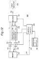
- the video signals thus written in the memory 90 as the line-sequential chrominance signals are reproduced by the playback unit 120 shown for example in FIG. 12.
- the FIG. 12 playback circuit 120 differs from the circuit configuration of FIG. 11 in that it has a sequential-line concurrent-combining circuit 138 for concurrently combining the color-difference signals R-Y and B-Y read out line-sequentially from the memory 90, while it does not have the matrix 126.
- the data of the color-difference signals R-Y and B-Y read out line-sequentially from the memory 90 are converted by the digital-to-analog converters 124 into corresponding analog signals while the chrominance signals of the lacking scanning lines are interpolated and concurrently combined with those of the existing scanning lines.
- the composite video signals are formed in the encoder 130 using these combined chrominance signals and the luminance signal Y so as to be issued at the output 132.
- FIG. 6 shows a still another alternative embodiment wherein the line sequencing circuit 72 is connected to the output lines 42 of the signal processing circuit 40 shown in FIG. 2.
- the line sequencing circuit 72 has two output lines 74 connected to the connector 74 through a switching circuit 78.
- the switching circuit 78 operates to select either one of two alternative connecting positions in response to the control output 60 of the control circuit 24. In this manner, the data of the luminance signal Y and the line-sequential color-difference signals R-Y and B-Y are written dot-sequentially in the memory 90.
- FIG. 7 shows an embodiment wherein the line sequencing circuit 72 is connected to the output lines 42 of the signal processing circuit 40 shown in FIG. 3.
- the line sequencing circuit 72 has two output lines 74 connected via two analog-to-digital converters 62 to the switching circuit 78.
- the line sequencing circuit 72 is an analog signal operational circuit adapted for sequencing the color-difference signals transmitted from the outputs 42 of the signal processing circuit 40 in the form of analog signals into scanning-line-sequential signals.
- the luminance signal Y and the line-sequential color-difference signals R-Y and B-Y, thus sequenced in the form of analog signals, are converted by the analog-to-digital converters 62 into corresponding digital signal data which are converted by the switching circuit 78 into dot-sequential signals for storage in the memory 90.
- FIG. 8 shows a further embodiment in which the line sequencing circuit 72 is connected to output lines 42 of the signal processing circuit 40 shown in FIG. 4.
- the circuit 72 has two output lines 74 connected to a switching circuit 78 the output 58 of which is connected by way of an analog-to-digital converter 68 to the data line 70 of the connector 14.
- the luminance signal Y and the line sequential color-difference signals R-Y and B-Y line-sequenced in the form of analog signals are converted by the switching circuit 78 into dot-sequential signals which are converted in the analog-to-digital converter 68 into corresponding digital data for storage ultimately in the memory 90.
- the video signals stored in this manner in the memory 90 are read out by the playback unit similar to that shown in FIG. 11 or 12 so as to be reproduced in the form of a visual image on an output device such as a video monitor 134.
Claims (7)
caractérisé en ce que :
Applications Claiming Priority (2)
| Application Number | Priority Date | Filing Date | Title |
|---|---|---|---|
| JP106239/87 | 1987-05-01 | ||
| JP62106239A JPH07110065B2 (ja) | 1987-05-01 | 1987-05-01 | デイジタル電子スチルカメラ |
Publications (2)
| Publication Number | Publication Date |
|---|---|
| EP0289944A1 EP0289944A1 (fr) | 1988-11-09 |
| EP0289944B1 true EP0289944B1 (fr) | 1992-07-22 |
Family
ID=14428564
Family Applications (1)
| Application Number | Title | Priority Date | Filing Date |
|---|---|---|---|
| EP88106858A Expired - Lifetime EP0289944B1 (fr) | 1987-05-01 | 1988-04-28 | Caméra électronique numérique d'images fixes utilisant l'accumulation des composants des signaux de vidéo dans une mémoire |
Country Status (4)
| Country | Link |
|---|---|
| US (1) | US4914746A (fr) |
| EP (1) | EP0289944B1 (fr) |
| JP (1) | JPH07110065B2 (fr) |
| DE (1) | DE3872929T2 (fr) |
Families Citing this family (37)
| Publication number | Priority date | Publication date | Assignee | Title |
|---|---|---|---|---|
| JP2878699B2 (ja) * | 1987-12-25 | 1999-04-05 | 株式会社東芝 | 電子カメラおよびその画像記録方法 |
| US5018017A (en) * | 1987-12-25 | 1991-05-21 | Kabushiki Kaisha Toshiba | Electronic still camera and image recording method thereof |
| US5034804A (en) * | 1987-12-25 | 1991-07-23 | Kabushiki Kaisha Toshiba | Electronic still camera with various modes of data compression |
| JP2931311B2 (ja) * | 1988-01-26 | 1999-08-09 | 富士写真フイルム株式会社 | ディジタル電子スチルカメラ |
| EP0372514B1 (fr) * | 1988-12-06 | 1997-03-05 | Canon Kabushiki Kaisha | Système pour prendre des images |
| US5008739A (en) * | 1989-02-13 | 1991-04-16 | Eastman Kodak Company | Real-time digital processor for producing full resolution color signals from a multi-color image sensor |
| US5187569A (en) * | 1989-03-03 | 1993-02-16 | Asahi Kogaku Kogyo Kabushiki Kaisha | Solid state imaging device and electronic still camera using same |
| JP2750602B2 (ja) * | 1989-03-03 | 1998-05-13 | 旭光学工業株式会社 | 固体撮像素子およびその素子を用いた電子スチルカメラ |
| US5206716A (en) * | 1989-04-28 | 1993-04-27 | Canon Kabushiki Kaisha | Camera having digital-to-analog converter with variably settable reference level |
| JP2703988B2 (ja) * | 1989-04-28 | 1998-01-26 | キヤノン株式会社 | カメラ |
| US5016107A (en) * | 1989-05-09 | 1991-05-14 | Eastman Kodak Company | Electronic still camera utilizing image compression and digital storage |
| US5231501A (en) * | 1989-05-25 | 1993-07-27 | Asahi Kogaku Kogyo Kabushiki Kaisha | Still video apparatus |
| FR2653291B1 (fr) * | 1989-05-25 | 1993-02-19 | Asahi Optical Co Ltd | Camera video fixe avec adaptateur amovible. |
| GB2234647B (en) * | 1989-05-25 | 1994-02-16 | Asahi Optical Co Ltd | Still video apparatus |
| EP0415756A3 (en) * | 1989-08-31 | 1991-12-27 | Canon Kabushiki Kaisha | Electronic still camera |
| EP0428310A3 (en) * | 1989-11-06 | 1992-08-05 | Canon Kabushiki Kaisha | Image processing apparatus and image transmitting apparatus |
| US5335072A (en) * | 1990-05-30 | 1994-08-02 | Minolta Camera Kabushiki Kaisha | Photographic system capable of storing information on photographed image data |
| EP0469804B1 (fr) * | 1990-07-30 | 1997-06-04 | Sony Corporation | Appareil pour l'enregistrement et/ou la reproduction de signaux vidéo |
| KR920005598A (ko) * | 1990-08-29 | 1992-03-28 | 오가 노리오 | 디지탈 전자스틸카메라 |
| EP0486310A3 (en) * | 1990-11-16 | 1993-01-27 | Canon Kabushiki Kaisha | Method and system for reproducing images |
| US5138459A (en) | 1990-11-20 | 1992-08-11 | Personal Computer Cameras, Inc. | Electronic still video camera with direct personal computer (pc) compatible digital format output |
| US5806072A (en) * | 1991-12-20 | 1998-09-08 | Olympus Optical Co., Ltd. | Electronic imaging apparatus having hierarchical image data storage structure for computer-compatible image data management |
| US5475441A (en) * | 1992-12-10 | 1995-12-12 | Eastman Kodak Company | Electronic camera with memory card interface to a computer |
| EP0683596B1 (fr) * | 1994-05-18 | 2000-08-30 | Sharp Kabushiki Kaisha | Caméra du type carte avec fonction de traitement d'image |
| US5832170A (en) * | 1994-12-16 | 1998-11-03 | Sony Corporation | Apparatus and method for storing and reproducing high-resolution video images |
| US6452632B1 (en) | 1997-01-31 | 2002-09-17 | Kabushiki Kaisha Toshiba | Solid state image sensor and video system using the same |
| US6738090B2 (en) | 1997-10-23 | 2004-05-18 | Eastman Kodak Company | System and method for using a single intelligence circuit for a plurality of imaging rendering components |
| US6587140B2 (en) | 1997-10-23 | 2003-07-01 | Eastman Kodak Company | System and method for using a single intelligence circuit in both a digital camera and printer |
| US7039869B2 (en) * | 2000-02-14 | 2006-05-02 | Fuji Photo Film Co., Ltd. | Global lab software |
| JP2002300384A (ja) * | 2001-03-30 | 2002-10-11 | Minolta Co Ltd | 画像復元装置、画像復元方法、プログラム及び記録媒体 |
| US20030078849A1 (en) * | 2001-10-23 | 2003-04-24 | Ncr Corporation | Self-checkout system having component video camera for produce purchase monitoring |
| US8525924B2 (en) | 2008-12-29 | 2013-09-03 | Red.Com, Inc. | Modular motion camera |
| WO2014144950A1 (fr) * | 2013-03-15 | 2014-09-18 | Olive Medical Corporation | Amélioration de bord sensible au bruit |
| US9681028B2 (en) | 2013-03-15 | 2017-06-13 | Red.Com, Inc. | Digital camera with wireless connectivity |
| ES2748454T3 (es) * | 2014-04-04 | 2020-03-16 | Red Com Llc | Módulo de difusión para cámara digital |
| KR20180093056A (ko) | 2015-12-14 | 2018-08-20 | 레드.컴, 엘엘씨 | 모듈형 디지털 카메라 및 셀룰러 폰 |
| JPWO2021256107A1 (fr) * | 2020-06-15 | 2021-12-23 |
Family Cites Families (29)
| Publication number | Priority date | Publication date | Assignee | Title |
|---|---|---|---|---|
| US4074324B1 (en) * | 1975-07-14 | 1994-01-11 | S. Barrett Jon | Instant electronic camera |
| JPS54140510A (en) * | 1978-04-23 | 1979-10-31 | Canon Inc | Image information recording and reproducing apparatus |
| JPS56109087A (en) * | 1980-01-31 | 1981-08-29 | Sony Corp | Digital color encoder |
| JPS5728480A (en) * | 1980-07-28 | 1982-02-16 | Hitachi Ltd | Pure electronic camera device |
| JPS5778286A (en) * | 1980-10-31 | 1982-05-15 | Nippon Kogaku Kk <Nikon> | Electronic camera |
| JPS5795777A (en) * | 1980-12-05 | 1982-06-14 | Fuji Photo Film Co Ltd | Video recorder |
| GB2089169A (en) * | 1980-12-10 | 1982-06-16 | Campbell Malcolm Gregory | An electronic camera |
| US4345270A (en) * | 1981-01-27 | 1982-08-17 | Sony Corporation | Solid state digital television camera |
| JPS587987A (ja) * | 1981-07-08 | 1983-01-17 | Oki Electric Ind Co Ltd | 固体写真装置 |
| JPS5842387A (ja) * | 1981-09-04 | 1983-03-11 | Victor Co Of Japan Ltd | デイジタル信号記録方式 |
| BE890517A (fr) * | 1981-09-28 | 1982-01-18 | Staar Sa | Dispositif de memorisation d'images electroniques |
| JPS58100590A (ja) * | 1981-12-11 | 1983-06-15 | Sony Corp | サンプリング出力の合成方法 |
| US4599657A (en) * | 1981-12-29 | 1986-07-08 | Canon Kabushiki Kaisha | Image pick-up device |
| JPS5970091A (ja) * | 1982-10-13 | 1984-04-20 | Nippon Kogaku Kk <Nikon> | 電子スチルカメラ |
| JPS5985196A (ja) * | 1982-11-06 | 1984-05-17 | Victor Co Of Japan Ltd | カラ−映像信号のデイジタル処理装置 |
| JPS5986987A (ja) * | 1982-11-10 | 1984-05-19 | Matsushita Electric Ind Co Ltd | カラ−カメラ装置 |
| JPS5989091A (ja) * | 1982-11-12 | 1984-05-23 | Matsushita Electric Ind Co Ltd | カラ−カメラ装置 |
| JPS59183592A (ja) * | 1983-04-04 | 1984-10-18 | Nippon Hoso Kyokai <Nhk> | 色分離情報を記憶させた電子スチルカメラ |
| JPS6038988A (ja) * | 1983-08-12 | 1985-02-28 | Victor Co Of Japan Ltd | 固体撮像素子を用いた静止画像撮像装置 |
| JPS6068793A (ja) * | 1983-09-26 | 1985-04-19 | Sony Corp | カラ−ビデオ信号のデイジタル化回路 |
| DE3511237A1 (de) * | 1984-03-29 | 1985-10-03 | Olympus Optical Co., Ltd., Tokio/Tokyo | Bildmarkierungsgeraet |
| US4646166A (en) * | 1984-07-25 | 1987-02-24 | Rca Corporation | Video still image storage system with high resolution |
| JPS6188688A (ja) * | 1984-10-08 | 1986-05-06 | Matsushita Electronics Corp | カラ−撮像装置 |
| JPS621373A (ja) * | 1985-06-27 | 1987-01-07 | Toshiba Corp | 画像符号化方式 |
| US4791479A (en) * | 1986-06-04 | 1988-12-13 | Olympus Optical Co., Ltd. | Color-image sensing apparatus |
| US4714963A (en) * | 1986-07-03 | 1987-12-22 | Eastman Kodak Company | Asynchronous still timing for a video camera producing movie or still images |
| JP2666260B2 (ja) * | 1986-11-12 | 1997-10-22 | 松下電器産業株式会社 | 電子スチルカメラ |
| JPS63262983A (ja) * | 1987-04-20 | 1988-10-31 | Nikon Corp | デイジタル電子スチルカメラ |
| US4803554A (en) * | 1987-09-30 | 1989-02-07 | Polaroid Corporation | Electronic imaging camera utilizing EPROM memory |
-
1987
- 1987-05-01 JP JP62106239A patent/JPH07110065B2/ja not_active Expired - Fee Related
-
1988
- 1988-04-28 EP EP88106858A patent/EP0289944B1/fr not_active Expired - Lifetime
- 1988-04-28 DE DE8888106858T patent/DE3872929T2/de not_active Expired - Lifetime
- 1988-04-29 US US07/188,403 patent/US4914746A/en not_active Expired - Lifetime
Also Published As
| Publication number | Publication date |
|---|---|
| US4914746A (en) | 1990-04-03 |
| JPS63274289A (ja) | 1988-11-11 |
| EP0289944A1 (fr) | 1988-11-09 |
| DE3872929D1 (de) | 1992-08-27 |
| JPH07110065B2 (ja) | 1995-11-22 |
| DE3872929T2 (de) | 1992-12-17 |
Similar Documents
| Publication | Publication Date | Title |
|---|---|---|
| EP0289944B1 (fr) | Caméra électronique numérique d'images fixes utilisant l'accumulation des composants des signaux de vidéo dans une mémoire | |
| EP0377025B1 (fr) | Dispositif de verification a faible resolution pour images video | |
| US4758883A (en) | Electronic picture camera with reduced memory capacity | |
| US5379069A (en) | Selectively operable plural imaging devices for use with a video recorder | |
| EP0101600B1 (fr) | Dispositif d'enregistrement de signal vidéo | |
| JP2001197371A (ja) | 撮像装置 | |
| JPH08172635A (ja) | 撮像装置 | |
| JP2013211645A (ja) | 画像処理装置 | |
| US5550586A (en) | Video camera and image input device connected through signal line for transferring multiplex data, and image input system using them | |
| US4982290A (en) | Digital electronic still camera effecting analog-to-digital conversion after color balance adjustment and gradation correction | |
| US6977683B1 (en) | Digital camera | |
| US5793923A (en) | Device for controlling number of pixels | |
| JPH02123879A (ja) | 交換レンズユニット及び撮像装置 | |
| US7286167B2 (en) | Digital camera recording dynamic range compression information | |
| JP2731523B2 (ja) | カメラシステム | |
| JP3059920B2 (ja) | 撮像装置 | |
| JPH0965345A (ja) | 電子スチルカメラ | |
| JP3059921B2 (ja) | 撮像装置 | |
| JPS63281595A (ja) | ディジタル電子スチルカメラ | |
| JP3451626B2 (ja) | ビデオカメラ | |
| JP2602949B2 (ja) | ビデオカメラ | |
| JP2976113B2 (ja) | スチルビデオカメラとその再生装置 | |
| JPH09270941A (ja) | 撮影映像に対するデータ重畳方法及び撮影装置 | |
| JPH07110066B2 (ja) | ディジタル電子スチルカメラ | |
| JP3276820B2 (ja) | 撮像装置 |
Legal Events
| Date | Code | Title | Description |
|---|---|---|---|
| PUAI | Public reference made under article 153(3) epc to a published international application that has entered the european phase |
Free format text: ORIGINAL CODE: 0009012 |
|
| AK | Designated contracting states |
Kind code of ref document: A1 Designated state(s): DE GB NL |
|
| 17P | Request for examination filed |
Effective date: 19890418 |
|
| 17Q | First examination report despatched |
Effective date: 19910326 |
|
| GRAA | (expected) grant |
Free format text: ORIGINAL CODE: 0009210 |
|
| AK | Designated contracting states |
Kind code of ref document: B1 Designated state(s): DE GB NL |
|
| REF | Corresponds to: |
Ref document number: 3872929 Country of ref document: DE Date of ref document: 19920827 |
|
| PLBE | No opposition filed within time limit |
Free format text: ORIGINAL CODE: 0009261 |
|
| STAA | Information on the status of an ep patent application or granted ep patent |
Free format text: STATUS: NO OPPOSITION FILED WITHIN TIME LIMIT |
|
| 26N | No opposition filed | ||
| REG | Reference to a national code |
Ref country code: GB Ref legal event code: IF02 |
|
| REG | Reference to a national code |
Ref country code: GB Ref legal event code: 732E |
|
| PGFP | Annual fee paid to national office [announced via postgrant information from national office to epo] |
Ref country code: NL Payment date: 20070424 Year of fee payment: 20 |
|
| PGFP | Annual fee paid to national office [announced via postgrant information from national office to epo] |
Ref country code: DE Payment date: 20070530 Year of fee payment: 20 |
|
| PGFP | Annual fee paid to national office [announced via postgrant information from national office to epo] |
Ref country code: GB Payment date: 20070430 Year of fee payment: 20 |
|
| REG | Reference to a national code |
Ref country code: GB Ref legal event code: PE20 Expiry date: 20080427 |
|
| PG25 | Lapsed in a contracting state [announced via postgrant information from national office to epo] |
Ref country code: NL Free format text: LAPSE BECAUSE OF EXPIRATION OF PROTECTION Effective date: 20080428 |
|
| NLV7 | Nl: ceased due to reaching the maximum lifetime of a patent |
Effective date: 20080428 |
|
| PG25 | Lapsed in a contracting state [announced via postgrant information from national office to epo] |
Ref country code: GB Free format text: LAPSE BECAUSE OF EXPIRATION OF PROTECTION Effective date: 20080427 |