EP0287337A2 - Programming circuit for programmable logic array I/O cell - Google Patents
Programming circuit for programmable logic array I/O cell Download PDFInfo
- Publication number
- EP0287337A2 EP0287337A2 EP88303292A EP88303292A EP0287337A2 EP 0287337 A2 EP0287337 A2 EP 0287337A2 EP 88303292 A EP88303292 A EP 88303292A EP 88303292 A EP88303292 A EP 88303292A EP 0287337 A2 EP0287337 A2 EP 0287337A2
- Authority
- EP
- European Patent Office
- Prior art keywords
- array
- output
- architecture
- programming
- programmable
- Prior art date
- Legal status (The legal status is an assumption and is not a legal conclusion. Google has not performed a legal analysis and makes no representation as to the accuracy of the status listed.)
- Granted
Links
Images
Classifications
-
- H—ELECTRICITY
- H03—ELECTRONIC CIRCUITRY
- H03K—PULSE TECHNIQUE
- H03K19/00—Logic circuits, i.e. having at least two inputs acting on one output; Inverting circuits
-
- H—ELECTRICITY
- H03—ELECTRONIC CIRCUITRY
- H03K—PULSE TECHNIQUE
- H03K19/00—Logic circuits, i.e. having at least two inputs acting on one output; Inverting circuits
- H03K19/02—Logic circuits, i.e. having at least two inputs acting on one output; Inverting circuits using specified components
- H03K19/173—Logic circuits, i.e. having at least two inputs acting on one output; Inverting circuits using specified components using elementary logic circuits as components
- H03K19/177—Logic circuits, i.e. having at least two inputs acting on one output; Inverting circuits using specified components using elementary logic circuits as components arranged in matrix form
- H03K19/17748—Structural details of configuration resources
- H03K19/17772—Structural details of configuration resources for powering on or off
-
- H—ELECTRICITY
- H03—ELECTRONIC CIRCUITRY
- H03K—PULSE TECHNIQUE
- H03K17/00—Electronic switching or gating, i.e. not by contact-making and –breaking
- H03K17/22—Modifications for ensuring a predetermined initial state when the supply voltage has been applied
-
- H—ELECTRICITY
- H03—ELECTRONIC CIRCUITRY
- H03K—PULSE TECHNIQUE
- H03K19/00—Logic circuits, i.e. having at least two inputs acting on one output; Inverting circuits
- H03K19/02—Logic circuits, i.e. having at least two inputs acting on one output; Inverting circuits using specified components
- H03K19/173—Logic circuits, i.e. having at least two inputs acting on one output; Inverting circuits using specified components using elementary logic circuits as components
- H03K19/177—Logic circuits, i.e. having at least two inputs acting on one output; Inverting circuits using specified components using elementary logic circuits as components arranged in matrix form
- H03K19/17704—Logic circuits, i.e. having at least two inputs acting on one output; Inverting circuits using specified components using elementary logic circuits as components arranged in matrix form the logic functions being realised by the interconnection of rows and columns
-
- H—ELECTRICITY
- H03—ELECTRONIC CIRCUITRY
- H03K—PULSE TECHNIQUE
- H03K19/00—Logic circuits, i.e. having at least two inputs acting on one output; Inverting circuits
- H03K19/02—Logic circuits, i.e. having at least two inputs acting on one output; Inverting circuits using specified components
- H03K19/173—Logic circuits, i.e. having at least two inputs acting on one output; Inverting circuits using specified components using elementary logic circuits as components
- H03K19/177—Logic circuits, i.e. having at least two inputs acting on one output; Inverting circuits using specified components using elementary logic circuits as components arranged in matrix form
- H03K19/17736—Structural details of routing resources
- H03K19/17744—Structural details of routing resources for input/output signals
-
- H—ELECTRICITY
- H03—ELECTRONIC CIRCUITRY
- H03K—PULSE TECHNIQUE
- H03K19/00—Logic circuits, i.e. having at least two inputs acting on one output; Inverting circuits
- H03K19/02—Logic circuits, i.e. having at least two inputs acting on one output; Inverting circuits using specified components
- H03K19/173—Logic circuits, i.e. having at least two inputs acting on one output; Inverting circuits using specified components using elementary logic circuits as components
- H03K19/177—Logic circuits, i.e. having at least two inputs acting on one output; Inverting circuits using specified components using elementary logic circuits as components arranged in matrix form
- H03K19/17748—Structural details of configuration resources
- H03K19/1776—Structural details of configuration resources for memories
Definitions
- the present invention relates to circuits for programming an output cell in a programmable logic device (PLD) circuit.
- PLD programmable logic device
- a typical PLD has an array of fuses or memory cells which can be programmed to configure the array to provide a number of desired logic functions. Often, this array will be used in conjunction with output cells which may include multiplexers, inverters or other circuitry for handling the outputs of the main fuse or memory array. One or more array outputs may be provided to each output cell. These output cells can have programmable elements in them, such as a multiplexer which can be programmed to select one or the other of its inputs. The programming data for the output cell is typically stored in separate fuses or memory cells. Because the output cells need to be programmed or configured properly prior to readout from the main array, these fuses or memory cells are physically located outside of the main array and next to the other logic elements of the output cell. This complicates the layout of a PLD chip and requires the duplication of sense amplifiers and addressing circuits which are used for the main array.
- the present invention is an improved architecture for programming an output cell (macro cell) in a PLD.
- the memory cells for the macro cell are stored in the main array itself.
- a power-on sense circuit senses the presence of power and enables an architecture portion of the main array while disabling the rest of the main array.
- the power-on sense signal also enables a path from the output of the array to the macro cell elements to be programmed. When the power-on sense signal is removed a short time after power-up, this path is blocked so that the array outputs continue on their normal path and the architecture portion of the array is disabled while the rest of the array is enabled for normal operation.
- the layout of the circuit is simplified and less circuitry is required for sense amplifiers and other circuits which are used commonly by elements of the array.
- the invention allows the placement of these memory cells in the main array by providing a power-on sense circuit which enables this portion of the array while disabling the logic portion of the array during a programming of the output cell architecture. The invention thus insures the architecture will be programmed upon each power-up of the circuit.
- the output cell has six programmable elements which include three multiplexers.
- Six programming inputs are provided from a logic circuit which decodes the signals of three output lines from the main memory array. These output lines are coupled to this logic circuit by transistors which have their gates connected to a power-on sense circuit. When the power-on sense signal is applied, these transistor switches couple the outputs to the logic circuit for programming.
- the power-on sense signal itself is a pulse which is provided when the power applied reaches a predetermined level.
- the power-on sense (POS) pulse is provided to a memory array logic circuit which provides four signals to the memory array. Two of those signals go to the architecture portion of the array and two go to the logic portion of the array. A first signal enables a transistor in each column line to activate that column line. A second signal disables a deactivating transistor which couples each column line to ground when not in use.
- POS power-on sense
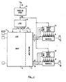
- Fig. 1 shows a memory array 10 having a logic portion 12 and an architecture portion 14. The outputs of this array are provided along output lines 16 to macro cells 18. The output of each macro cell is coupled to an I/O pin 20.
- Memory array 10 typically contains a crisscrossing pattern of lines which can be connected via programmable "fuses" to produce a variety of logic functions.
- the fuse is often an actual metal fuse which can be blown or a transistor which is controlled by a programmable memory cell to either provide a connection or not provide a connection.
- An example of such an array is shown in co-pending application Serial No. 856,539 entitled “Single Function Programmable Logic Array Circuit", filed April 25, 1986, and incorporated herein by reference.
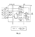
- each macro cell 18 has the elements shown in Fig. 2.
- Macro cell 18 is provided with three outputs 16 from the array and also provides two feedback lines 22 to the array.
- macro cell 18 contains a J-K latch 24, multiplexers 26, 28 and 30, polarity control elements (PCE) 32, 34 and 36 and a tri-state buffer 38.
- PCE polarity control elements
- Each PCE either inverts the signal or leaves the signal unchanged, and can be constructed with a multiplexer having one input inverted and the other not inverted.
- output cell can perform several different functions.
- one of the output lines 16 can simply be provided to output pad 20.
- output pad 20 can be used as an input pad.
- the output of latch 24 can be provided to output pad 20.
- Other configurations are available as well.
- a power-on sense circuit 40 which determines when power line 42 reaches a predetermined level and sends out a power-on sense (POS) pulse.
- the POS pulse is provided to a logic circuit 44 which provides a pair of control signals 46, 48 to the architecture portion 14 of memory array 10. Another pair of control signals 50, 52 are provided to logic portion 12 of memory array 10.
- signal lines 46 and 48 enable portion 14 while lines 50 and 52 disable portion 12.
- the outputs of architecture portion 14 are then provided on output lines 16 to macro cells 18.
- These signals are also provided to logic circuits 54 which are enabled by the POS signal.
- Logic circuits 54 provide the programming inputs to macro cells 18. After programming, the POS pulse disappears, logic circuits 54 are disabled, architecture portion 14 of array 10 is disabled and logic portion 12 of array 10 is enabled. Thereafter, operation of the circuit continues in a normal manner.
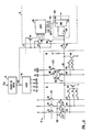
- Fig. 3 shows the enabling and disabling lines of Fig. 1 in more detail.
- a single output line 16 is shown which is provided from a term line 56 through a sense amplifier 58.
- Term line 56 is programmed from a number of column lines as discussed in co-pending application Serial No. 856,539.
- a single such connection is shown in Fig. 3 being made through a transistor 60 which is coupled to column lines 62, 64 and 66 through programming transistors. This type of connection is shown in detail in co-pending application Serial No. 856,623 entitled “Programmable Matrix Circuit", filed April 25, 1986, and incorporated herein by reference.
- the three column lines 62, 64 and 66 are enabled by a signal CS1 from logic circuit 44 which is provided to three transistors 68, 70 and 72.
- CS1 when CS1 is a logic high, these transistors are enabled, and signals A, A and X are allowed to propagate to nodes 66, 64 and 62, respectively.
- CS2 is held at zero, turning off transistors 78, 76 and 74.
- CS1 must equal 1 and CS2 must equal 0.
- these column lines will be disabled by being pulled to ground potential by transistors 74, 76 and 78.
- a pair of column lines 80, 82 are coupled via a transistor 84 to term line 56.
- signals CS3 and CS4 enabled transistors 86, 88 and 90, 92, respectively.
- D0 and D1 are preset to ground and +V, respectively.
- the transistors coupled to transistor 84 are then programmed to connect node 56 (through transistor 84) to either line 80 (ground) or line 82 (+V) to give a logic 0 or 1.
- Signals CS1-CS4 are decoded by logic circuit 44 from the POS signal from power-on sense circuit 40.
- the POS signal is a logic pulse, which when high enables array portion 14 and disables array portion 12.
- the POS signal is similarly provided to transistors 94, 96 and 98 in output cell 18. These transistors enable output lines 16 to be coupled to a logic circuit 100.
- Logic circuit 100 provides seven outputs 102, 103 to the various programmable elements of output cell 18. Six output lines 16 are coupled to logic circuit 100, which has seven outputs, three outputs 102 and four outputs 103.
- Logic circuit 100 includes a 3 to 4 encoder for providing four outputs 103 from three of inputs 16. Outputs 103 control multiplexers 26, 28 and 30 of Fig. 2. Multiplexer 30 requires two control signals because it is a 3 position multiplexer.
- the outputs 102 of logic circuit 100 are each coupled to a polarity control element 104 of Fig. 3. Polarity control element 104 shown in Fig. 3 consists of a multiplexer 106 and an inverter 108. The output of polarity control element 104 will either be the non-inverted or inverted signal on line 16 depending upon the state of the signal provided to the select input
- the remaining lines 102 are similarly provided to the other programmable elements of output cell 18.
- the layout of the circuit is simplified since this memory cell is simply another cell in the array.
- the need for a separate sense amplifier 58 and separate addressing circuitry is eliminated. If memory cell 84 were contained in output cell 18, such a separate sense amplifier and addressing circuit would be necessary.
Landscapes
- Physics & Mathematics (AREA)
- Mathematical Physics (AREA)
- Engineering & Computer Science (AREA)
- Computer Hardware Design (AREA)
- Computing Systems (AREA)
- General Engineering & Computer Science (AREA)
- Computer Networks & Wireless Communication (AREA)
- Logic Circuits (AREA)
- Design And Manufacture Of Integrated Circuits (AREA)
Abstract
Description
- The present invention relates to circuits for programming an output cell in a programmable logic device (PLD) circuit.
- A typical PLD has an array of fuses or memory cells which can be programmed to configure the array to provide a number of desired logic functions. Often, this array will be used in conjunction with output cells which may include multiplexers, inverters or other circuitry for handling the outputs of the main fuse or memory array. One or more array outputs may be provided to each output cell. These output cells can have programmable elements in them, such as a multiplexer which can be programmed to select one or the other of its inputs. The programming data for the output cell is typically stored in separate fuses or memory cells. Because the output cells need to be programmed or configured properly prior to readout from the main array, these fuses or memory cells are physically located outside of the main array and next to the other logic elements of the output cell. This complicates the layout of a PLD chip and requires the duplication of sense amplifiers and addressing circuits which are used for the main array.
- The present invention is an improved architecture for programming an output cell (macro cell) in a PLD. The memory cells for the macro cell are stored in the main array itself. Upon power-up, a power-on sense circuit senses the presence of power and enables an architecture portion of the main array while disabling the rest of the main array. The power-on sense signal also enables a path from the output of the array to the macro cell elements to be programmed. When the power-on sense signal is removed a short time after power-up, this path is blocked so that the array outputs continue on their normal path and the architecture portion of the array is disabled while the rest of the array is enabled for normal operation.
- By storing the memory cells for the output cell in the array, the layout of the circuit is simplified and less circuitry is required for sense amplifiers and other circuits which are used commonly by elements of the array. The invention allows the placement of these memory cells in the main array by providing a power-on sense circuit which enables this portion of the array while disabling the logic portion of the array during a programming of the output cell architecture. The invention thus insures the architecture will be programmed upon each power-up of the circuit.
- In one embodiment, the output cell has six programmable elements which include three multiplexers. Six programming inputs are provided from a logic circuit which decodes the signals of three output lines from the main memory array. These output lines are coupled to this logic circuit by transistors which have their gates connected to a power-on sense circuit. When the power-on sense signal is applied, these transistor switches couple the outputs to the logic circuit for programming. The power-on sense signal itself is a pulse which is provided when the power applied reaches a predetermined level.
- Similarly, the power-on sense (POS) pulse is provided to a memory array logic circuit which provides four signals to the memory array. Two of those signals go to the architecture portion of the array and two go to the logic portion of the array. A first signal enables a transistor in each column line to activate that column line. A second signal disables a deactivating transistor which couples each column line to ground when not in use.
- For a fuller understanding of the nature and advantages of the invention, reference should be made to the ensuing detailed description taken in conjunction with the accompanying drawings.
-
- Fig. 1 is a block diagram of a programming circuit for an output cell according to the present invention;
- Fig. 2 is a block diagram of a typical output cell; and
- Fig. 3 is a combination block and schematic diagram showing a portion of the circuit of Fig. 1 in more detail.
- Fig. 1 shows a
memory array 10 having alogic portion 12 and anarchitecture portion 14. The outputs of this array are provided alongoutput lines 16 tomacro cells 18. The output of each macro cell is coupled to an I/O pin 20. -
Memory array 10 typically contains a crisscrossing pattern of lines which can be connected via programmable "fuses" to produce a variety of logic functions. The fuse is often an actual metal fuse which can be blown or a transistor which is controlled by a programmable memory cell to either provide a connection or not provide a connection. An example of such an array is shown in co-pending application Serial No. 856,539 entitled "Single Function Programmable Logic Array Circuit", filed April 25, 1986, and incorporated herein by reference. - In one embodiment, each
macro cell 18 has the elements shown in Fig. 2. Macrocell 18 is provided with threeoutputs 16 from the array and also provides twofeedback lines 22 to the array. Internally,macro cell 18 contains aJ-K latch 24,multiplexers buffer 38. Each PCE either inverts the signal or leaves the signal unchanged, and can be constructed with a multiplexer having one input inverted and the other not inverted. - These six programmable circuits allow the output cell to perform several different functions. In one state, one of the
output lines 16 can simply be provided tooutput pad 20. In another configuration,output pad 20 can be used as an input pad. In still another configuration, the output oflatch 24 can be provided tooutput pad 20. Other configurations are available as well. - Returning to Fig. 1, it can be seen that it is desirable to program
macro cell 18 prior to reading the logic fromarray 10. This is accomplished with a power-onsense circuit 40 which determines when power line 42 reaches a predetermined level and sends out a power-on sense (POS) pulse. The POS pulse is provided to alogic circuit 44 which provides a pair ofcontrol signals architecture portion 14 ofmemory array 10. Another pair ofcontrol signals logic portion 12 ofmemory array 10. When the POS signal is provided,signal lines portion 14 whilelines portion 12. The outputs ofarchitecture portion 14 are then provided onoutput lines 16 tomacro cells 18. These signals are also provided tologic circuits 54 which are enabled by the POS signal.Logic circuits 54 provide the programming inputs tomacro cells 18. After programming, the POS pulse disappears,logic circuits 54 are disabled,architecture portion 14 ofarray 10 is disabled andlogic portion 12 ofarray 10 is enabled. Thereafter, operation of the circuit continues in a normal manner. - Fig. 3 shows the enabling and disabling lines of Fig. 1 in more detail. A
single output line 16 is shown which is provided from aterm line 56 through a sense amplifier 58.Term line 56 is programmed from a number of column lines as discussed in co-pending application Serial No. 856,539. A single such connection is shown in Fig. 3 being made through atransistor 60 which is coupled to column lines 62, 64 and 66 through programming transistors. This type of connection is shown in detail in co-pending application Serial No. 856,623 entitled "Programmable Matrix Circuit", filed April 25, 1986, and incorporated herein by reference. The three column lines 62, 64 and 66 are enabled by a signal CS1 fromlogic circuit 44 which is provided to threetransistors A and X are allowed to propagate to nodes 66, 64 and 62, respectively. During this time CS2 is held at zero, turning offtransistors 78, 76 and 74. As can be seen, for the column lines to be enabled CS1 must equal 1 and CS2 must equal 0. When the opposite is the case, these column lines will be disabled by being pulled to ground potential bytransistors 74, 76 and 78. - Similarly, in output
cell architecture portion 14 ofmemory array 10, a pair of column lines 80, 82 are coupled via atransistor 84 toterm line 56. Similarly, signals CS3 and CS4 enabledtransistors transistor 84 are then programmed to connect node 56 (through transistor 84) to either line 80 (ground) or line 82 (+V) to give alogic - Signals CS1-CS4 are decoded by
logic circuit 44 from the POS signal from power-onsense circuit 40. The POS signal is a logic pulse, which when high enablesarray portion 14 and disablesarray portion 12. These signals oflogic circuit 44 are generated according to the following table:
- The POS signal is similarly provided to
transistors output cell 18. These transistors enableoutput lines 16 to be coupled to alogic circuit 100.Logic circuit 100 provides sevenoutputs output cell 18. Sixoutput lines 16 are coupled tologic circuit 100, which has seven outputs, threeoutputs 102 and fouroutputs 103.Logic circuit 100 includes a 3 to 4 encoder for providing fouroutputs 103 from three ofinputs 16.Outputs 103control multiplexers Multiplexer 30 requires two control signals because it is a 3 position multiplexer. Theoutputs 102 oflogic circuit 100 are each coupled to apolarity control element 104 of Fig. 3.Polarity control element 104 shown in Fig. 3 consists of amultiplexer 106 and aninverter 108. The output ofpolarity control element 104 will either be the non-inverted or inverted signal online 16 depending upon the state of the signal provided to theselect input 110 onsignal line 102. - The remaining
lines 102 are similarly provided to the other programmable elements ofoutput cell 18. - As can be seen, by using the memory cell of
transistor 84 in the memory array, the layout of the circuit is simplified since this memory cell is simply another cell in the array. In addition, the need for a separate sense amplifier 58 and separate addressing circuitry is eliminated. Ifmemory cell 84 were contained inoutput cell 18, such a separate sense amplifier and addressing circuit would be necessary. - As will be understood by those familiar with the art, the present invention may be embodied in other specific forms without departing from the spirit or essential characteristics thereof. For example, a different type of memory array, such as one requiring dedicated OR and AND gates, could be used. Alternately,
output cell 18 could be of any configuration having a programmable element in it and any number of such programmable elements could be present. Accordingly, the disclosure of the preferred embodiment of the invention is intended to be illustrative, but not limiting, of the scope of the invention which is set forth in the following claims.
Claims (10)
an array of programmable memory elements;
at least one output cell coupled to at least a portion of said array for providing an output from said array to an output terminal, said output cell having at least one programmable circuit with a programming input;
means for generating an architecture programming signal; and
means, coupled between said means for generating and at least a first one of said memory elements and responsive to said architecture programming signal, for providing an output of said array to said programming input of said programmable circuit.
means, responsive to said architecture programming signal, for enabling said architecture portion of said array and disabling said logic portion of said array.
an array of programmable memory elements with a logic portion containing a plurality of said memory elements for normal operation of said circuit and an architecture portion;
a plurality of output cells, each output cell being coupled to a plurality of output lines from said array for providing an output from said array to an output terminal and including a plurality of programmable circuits, each said programmable circuit having a programming input;
power-on sense means for detecting when a power supply level for said programmable logic array circuit passes a predetermined threshold value and generating a pulse signal;
means, responsive to said pulse signal, for enabling said architecture portion of said array and disabling said logic portion of said array;
a plurality of logic means, coupled between said output lines and said programmable circuits, for decoding signals from said architecture portion on said output lines and providing signals to said programming inputs; and
means, coupled between said power-on sense means and said logic means, for enabling said logic means responsive to said pulse signal.
programming an architecture element in said array;
detecting a power supply level for said array exceeding a predetermined value;
generating a power-on sense pulse when said power supply level exceeds said predetermined value; and
providing a signal from an output of said architecture element of said array to said programming input subsequent to said power-on sense pulse.
dividing said array into a logic portion containing a plurality of memory elements coupled to said output cell for normal operation of said circuit and an architecture portion containing said architecture element;
disabling said logic portion of said array responsive to said power-on sense pulse; and
enabling said architecture portion of said array responsive to said power-on sense pulse.
Priority Applications (1)
| Application Number | Priority Date | Filing Date | Title |
|---|---|---|---|
| AT88303292T ATE94705T1 (en) | 1987-04-14 | 1988-04-13 | PROGRAMMING CIRCUIT FOR INPUT/OUTPUT CELL OF PROGRAMMABLE LOGIC ARRAY. |
Applications Claiming Priority (2)
| Application Number | Priority Date | Filing Date | Title |
|---|---|---|---|
| US38101 | 1979-05-11 | ||
| US07/038,101 US4783606A (en) | 1987-04-14 | 1987-04-14 | Programming circuit for programmable logic array I/O cell |
Publications (3)
| Publication Number | Publication Date |
|---|---|
| EP0287337A2 true EP0287337A2 (en) | 1988-10-19 |
| EP0287337A3 EP0287337A3 (en) | 1989-07-26 |
| EP0287337B1 EP0287337B1 (en) | 1993-09-15 |
Family
ID=21898099
Family Applications (1)
| Application Number | Title | Priority Date | Filing Date |
|---|---|---|---|
| EP88303292A Expired - Lifetime EP0287337B1 (en) | 1987-04-14 | 1988-04-13 | Programming circuit for programmable logic array i/o cell |
Country Status (6)
| Country | Link |
|---|---|
| US (1) | US4783606A (en) |
| EP (1) | EP0287337B1 (en) |
| JP (1) | JP2571257B2 (en) |
| KR (1) | KR910001381B1 (en) |
| AT (1) | ATE94705T1 (en) |
| DE (1) | DE3884037T2 (en) |
Cited By (4)
| Publication number | Priority date | Publication date | Assignee | Title |
|---|---|---|---|---|
| EP0307912A3 (en) * | 1987-09-18 | 1989-07-12 | Fujitsu Limited | Programmable logic device |
| EP0406996A1 (en) * | 1989-06-21 | 1991-01-09 | Kawasaki Steel Corporation | Integrated circuit including programmable circuit |
| EP0420390A3 (en) * | 1989-09-29 | 1991-09-04 | Sgs-Thomson Microelectronics, Inc. (A Delaware Corp.) | Configuration memory for programmable logic device |
| EP0536756B1 (en) * | 1991-10-09 | 1998-05-27 | Rohm Co., Ltd. | A microcomputer and its option setting circuit |
Families Citing this family (36)
| Publication number | Priority date | Publication date | Assignee | Title |
|---|---|---|---|---|
| JP2582250B2 (en) * | 1986-10-03 | 1997-02-19 | 日本電信電話株式会社 | Timing signal delay circuit device |
| US4918641A (en) * | 1987-08-26 | 1990-04-17 | Ict International Cmos Technology, Inc. | High-performance programmable logic device |
| US5046035A (en) * | 1987-08-26 | 1991-09-03 | Ict International Cmos Tech., Inc. | High-performance user programmable logic device (PLD) |
| JPH0197016A (en) * | 1987-10-09 | 1989-04-14 | Fujitsu Ltd | Semiconductor integrated circuit device |
| KR910003593B1 (en) * | 1987-12-30 | 1991-06-07 | 삼성전자 주식회사 | Mode selection circuit for high integrated memory |
| JPH01208012A (en) * | 1988-02-15 | 1989-08-22 | Nec Corp | Flip-flop circuit |
| US4879481A (en) * | 1988-09-02 | 1989-11-07 | Cypress Semiconductor Corporation | Dual I/O macrocell for high speed synchronous state machine |
| US5023484A (en) * | 1988-09-02 | 1991-06-11 | Cypress Semiconductor Corporation | Architecture of high speed synchronous state machine |
| US4914322A (en) * | 1988-12-16 | 1990-04-03 | Advanced Micro Devices, Inc. | Polarity option control logic for use with a register of a programmable logic array macrocell |
| EP0373831A3 (en) * | 1988-12-16 | 1991-09-04 | Advanced Micro Devices, Inc. | Self latching logic gate |
| US4963769A (en) * | 1989-05-08 | 1990-10-16 | Cypress Semiconductor | Circuit for selective power-down of unused circuitry |
| US4940909A (en) * | 1989-05-12 | 1990-07-10 | Plus Logic, Inc. | Configuration control circuit for programmable logic devices |
| US5051622A (en) * | 1989-11-08 | 1991-09-24 | Chips And Technologies, Inc. | Power-on strap inputs |
| US5264742A (en) * | 1990-01-09 | 1993-11-23 | Sgs-Thomson Microelectronics, S.A. | Security locks for integrated circuit |
| FR2656939B1 (en) * | 1990-01-09 | 1992-04-03 | Sgs Thomson Microelectronics | SAFETY LATCHES FOR INTEGRATED CIRCUIT. |
| JP2544020B2 (en) * | 1990-11-19 | 1996-10-16 | 川崎製鉄株式会社 | Programmable logic element |
| JPH04192350A (en) * | 1990-11-24 | 1992-07-10 | Nec Corp | Semiconductor integrated circuit device |
| US5138198A (en) * | 1991-05-03 | 1992-08-11 | Lattice Semiconductor Corporation | Integrated programmable logic device with control circuit to power down unused sense amplifiers |
| US20020130681A1 (en) * | 1991-09-03 | 2002-09-19 | Cliff Richard G. | Programmable logic array integrated circuits |
| US6759870B2 (en) | 1991-09-03 | 2004-07-06 | Altera Corporation | Programmable logic array integrated circuits |
| JP2965802B2 (en) * | 1991-12-19 | 1999-10-18 | 株式会社東芝 | Semiconductor integrated circuit |
| JPH06176175A (en) * | 1992-12-10 | 1994-06-24 | Rohm Co Ltd | Option setting circuit and electronic equipment |
| US5332929A (en) * | 1993-04-08 | 1994-07-26 | Xilinx, Inc. | Power management for programmable logic devices |
| US5414380A (en) * | 1993-04-19 | 1995-05-09 | Motorola, Inc. | Integrated circuit with an active-level configurable and method therefor |
| US5453706A (en) * | 1994-04-01 | 1995-09-26 | Xilinx, Inc. | Field programmable gate array providing contention free configuration and reconfiguration |
| US5543730A (en) * | 1995-05-17 | 1996-08-06 | Altera Corporation | Techniques for programming programmable logic array devices |
| US5625301A (en) * | 1995-05-18 | 1997-04-29 | Actel Corporation | Flexible FPGA input/output architecture |
| US5629635A (en) * | 1995-09-26 | 1997-05-13 | Ics Technologies, Inc. | Address programming via LED pin |
| US5650734A (en) * | 1995-12-11 | 1997-07-22 | Altera Corporation | Programming programmable transistor devices using state machines |
| US6384630B2 (en) | 1996-06-05 | 2002-05-07 | Altera Corporation | Techniques for programming programmable logic array devices |
| US5959466A (en) | 1997-01-31 | 1999-09-28 | Actel Corporation | Field programmable gate array with mask programmed input and output buffers |
| US6150837A (en) * | 1997-02-28 | 2000-11-21 | Actel Corporation | Enhanced field programmable gate array |
| US6720796B1 (en) | 2001-05-06 | 2004-04-13 | Altera Corporation | Multiple size memories in a programmable logic device |
| US7111110B1 (en) * | 2002-12-10 | 2006-09-19 | Altera Corporation | Versatile RAM for programmable logic device |
| US7249213B2 (en) * | 2003-08-18 | 2007-07-24 | Silicon Storage Technology, Inc. | Memory device operable with a plurality of protocols with configuration data stored in non-volatile storage elements |
| US7893772B1 (en) | 2007-12-03 | 2011-02-22 | Cypress Semiconductor Corporation | System and method of loading a programmable counter |
Family Cites Families (10)
| Publication number | Priority date | Publication date | Assignee | Title |
|---|---|---|---|---|
| US4458163A (en) * | 1981-07-20 | 1984-07-03 | Texas Instruments Incorporated | Programmable architecture logic |
| JPS5961046A (en) * | 1982-09-30 | 1984-04-07 | Fujitsu Ltd | Integrated circuit device |
| US4609838A (en) * | 1984-05-30 | 1986-09-02 | Vlsi Technology, Inc. | Programmable array combinatorial (PAC) circuitry |
| DE3582990D1 (en) * | 1984-09-28 | 1991-07-04 | Advanced Micro Devices Inc | LOGIC CIRCUIT WITH DYNAMICALLY CONTROLLED OUTPUT. |
| US4684830A (en) * | 1985-03-22 | 1987-08-04 | Monolithic Memories, Inc. | Output circuit for a programmable logic array |
| US4634904A (en) * | 1985-04-03 | 1987-01-06 | Lsi Logic Corporation | CMOS power-on reset circuit |
| US4677318A (en) * | 1985-04-12 | 1987-06-30 | Altera Corporation | Programmable logic storage element for programmable logic devices |
| GB8518692D0 (en) * | 1985-07-24 | 1985-08-29 | Gen Electric Co Plc | Power-on reset circuit arrangements |
| US4771285A (en) * | 1985-11-05 | 1988-09-13 | Advanced Micro Devices, Inc. | Programmable logic cell with flexible clocking and flexible feedback |
| US4697097A (en) * | 1986-04-12 | 1987-09-29 | Motorola, Inc. | CMOS power-on detection circuit |
-
1987
- 1987-04-14 US US07/038,101 patent/US4783606A/en not_active Expired - Lifetime
-
1988
- 1988-04-13 DE DE88303292T patent/DE3884037T2/en not_active Expired - Lifetime
- 1988-04-13 KR KR1019880004162A patent/KR910001381B1/en not_active Expired
- 1988-04-13 AT AT88303292T patent/ATE94705T1/en not_active IP Right Cessation
- 1988-04-13 EP EP88303292A patent/EP0287337B1/en not_active Expired - Lifetime
- 1988-04-14 JP JP63090426A patent/JP2571257B2/en not_active Expired - Lifetime
Cited By (5)
| Publication number | Priority date | Publication date | Assignee | Title |
|---|---|---|---|---|
| EP0307912A3 (en) * | 1987-09-18 | 1989-07-12 | Fujitsu Limited | Programmable logic device |
| EP0406996A1 (en) * | 1989-06-21 | 1991-01-09 | Kawasaki Steel Corporation | Integrated circuit including programmable circuit |
| US5058074A (en) * | 1989-06-21 | 1991-10-15 | Kawasaki Steel Corporation | Integrated circuit including programmable circuit |
| EP0420390A3 (en) * | 1989-09-29 | 1991-09-04 | Sgs-Thomson Microelectronics, Inc. (A Delaware Corp.) | Configuration memory for programmable logic device |
| EP0536756B1 (en) * | 1991-10-09 | 1998-05-27 | Rohm Co., Ltd. | A microcomputer and its option setting circuit |
Also Published As
| Publication number | Publication date |
|---|---|
| KR910001381B1 (en) | 1991-03-04 |
| US4783606A (en) | 1988-11-08 |
| EP0287337A3 (en) | 1989-07-26 |
| EP0287337B1 (en) | 1993-09-15 |
| JP2571257B2 (en) | 1997-01-16 |
| ATE94705T1 (en) | 1993-10-15 |
| DE3884037D1 (en) | 1993-10-21 |
| JPS6447126A (en) | 1989-02-21 |
| DE3884037T2 (en) | 1994-04-14 |
| KR880013322A (en) | 1988-11-30 |
Similar Documents
| Publication | Publication Date | Title |
|---|---|---|
| EP0287337A2 (en) | Programming circuit for programmable logic array I/O cell | |
| US5128559A (en) | Logic block for programmable logic devices | |
| US4975601A (en) | User-writable random access memory logic block for programmable logic devices | |
| USRE37195E1 (en) | Programmable switch for FPGA input/output signals | |
| US4684830A (en) | Output circuit for a programmable logic array | |
| EP0448879B1 (en) | SRAM based cell for programmable logic devices | |
| US5450022A (en) | Structure and method for configuration of a field programmable gate array | |
| US4933577A (en) | Output circuit for a programmable logic array | |
| EP0582660B1 (en) | Device and method for multiplexing pins for in-system programming | |
| EP0351984B1 (en) | Programmable interface for computer system peripheral circuit card | |
| US5121359A (en) | Configuration memory for programmable logic device | |
| US4538245A (en) | Enabling circuit for redundant word lines in a semiconductor memory array | |
| US4959564A (en) | Sense amplifier power down circuitry for programmable logic device | |
| JPH05276007A (en) | Integrated circuit device | |
| EP0898281B1 (en) | Static random access memory circuits | |
| JPS6124329A (en) | Program array logic circuit including inspecting and provingcircuit | |
| US4930107A (en) | Method and apparatus for programming and verifying programmable elements in programmable devices | |
| JPH0197016A (en) | Semiconductor integrated circuit device | |
| US4796229A (en) | Writable logic array | |
| US4458163A (en) | Programmable architecture logic | |
| JPH06303128A (en) | Reprogrammable connection architecture using less storage cell than switch | |
| US5099453A (en) | Configuration memory for programmable logic device | |
| US5003202A (en) | Coincidence extendable programmable logic device | |
| EP0419760A2 (en) | Zero standby power, radiation hardened, memory redundancy circuit | |
| US5426432A (en) | IC card |
Legal Events
| Date | Code | Title | Description |
|---|---|---|---|
| PUAI | Public reference made under article 153(3) epc to a published international application that has entered the european phase |
Free format text: ORIGINAL CODE: 0009012 |
|
| AK | Designated contracting states |
Kind code of ref document: A2 Designated state(s): AT DE FR GB IT NL |
|
| PUAL | Search report despatched |
Free format text: ORIGINAL CODE: 0009013 |
|
| AK | Designated contracting states |
Kind code of ref document: A3 Designated state(s): AT DE FR GB IT NL |
|
| 17P | Request for examination filed |
Effective date: 19900124 |
|
| RAP1 | Party data changed (applicant data changed or rights of an application transferred) |
Owner name: ROHM CORPORATION |
|
| 17Q | First examination report despatched |
Effective date: 19911018 |
|
| GRAA | (expected) grant |
Free format text: ORIGINAL CODE: 0009210 |
|
| AK | Designated contracting states |
Kind code of ref document: B1 Designated state(s): AT DE FR GB IT NL |
|
| REF | Corresponds to: |
Ref document number: 94705 Country of ref document: AT Date of ref document: 19931015 Kind code of ref document: T |
|
| ITF | It: translation for a ep patent filed | ||
| REF | Corresponds to: |
Ref document number: 3884037 Country of ref document: DE Date of ref document: 19931021 |
|
| ET | Fr: translation filed | ||
| PG25 | Lapsed in a contracting state [announced via postgrant information from national office to epo] |
Ref country code: AT Effective date: 19940413 |
|
| PLBE | No opposition filed within time limit |
Free format text: ORIGINAL CODE: 0009261 |
|
| STAA | Information on the status of an ep patent application or granted ep patent |
Free format text: STATUS: NO OPPOSITION FILED WITHIN TIME LIMIT |
|
| 26N | No opposition filed | ||
| PG25 | Lapsed in a contracting state [announced via postgrant information from national office to epo] |
Ref country code: NL Effective date: 19941101 |
|
| NLV4 | Nl: lapsed or anulled due to non-payment of the annual fee | ||
| PGFP | Annual fee paid to national office [announced via postgrant information from national office to epo] |
Ref country code: FR Payment date: 20010409 Year of fee payment: 14 |
|
| PGFP | Annual fee paid to national office [announced via postgrant information from national office to epo] |
Ref country code: GB Payment date: 20010411 Year of fee payment: 14 |
|
| REG | Reference to a national code |
Ref country code: GB Ref legal event code: IF02 |
|
| PG25 | Lapsed in a contracting state [announced via postgrant information from national office to epo] |
Ref country code: GB Free format text: LAPSE BECAUSE OF NON-PAYMENT OF DUE FEES Effective date: 20020413 |
|
| GBPC | Gb: european patent ceased through non-payment of renewal fee |
Effective date: 20020413 |
|
| PG25 | Lapsed in a contracting state [announced via postgrant information from national office to epo] |
Ref country code: FR Free format text: LAPSE BECAUSE OF NON-PAYMENT OF DUE FEES Effective date: 20021231 |
|
| REG | Reference to a national code |
Ref country code: FR Ref legal event code: ST |
|
| PG25 | Lapsed in a contracting state [announced via postgrant information from national office to epo] |
Ref country code: IT Free format text: LAPSE BECAUSE OF NON-PAYMENT OF DUE FEES;WARNING: LAPSES OF ITALIAN PATENTS WITH EFFECTIVE DATE BEFORE 2007 MAY HAVE OCCURRED AT ANY TIME BEFORE 2007. THE CORRECT EFFECTIVE DATE MAY BE DIFFERENT FROM THE ONE RECORDED. Effective date: 20050413 |
|
| PGFP | Annual fee paid to national office [announced via postgrant information from national office to epo] |
Ref country code: DE Payment date: 20070405 Year of fee payment: 20 |