EP0283235B1 - Liquid crystal display device - Google Patents
Liquid crystal display device Download PDFInfo
- Publication number
- EP0283235B1 EP0283235B1 EP88302226A EP88302226A EP0283235B1 EP 0283235 B1 EP0283235 B1 EP 0283235B1 EP 88302226 A EP88302226 A EP 88302226A EP 88302226 A EP88302226 A EP 88302226A EP 0283235 B1 EP0283235 B1 EP 0283235B1
- Authority
- EP
- European Patent Office
- Prior art keywords
- display
- display region
- region
- electrodes
- liquid crystal
- Prior art date
- Legal status (The legal status is an assumption and is not a legal conclusion. Google has not performed a legal analysis and makes no representation as to the accuracy of the status listed.)
- Expired - Lifetime
Links
Images


Classifications
-
- G—PHYSICS
- G02—OPTICS
- G02F—OPTICAL DEVICES OR ARRANGEMENTS FOR THE CONTROL OF LIGHT BY MODIFICATION OF THE OPTICAL PROPERTIES OF THE MEDIA OF THE ELEMENTS INVOLVED THEREIN; NON-LINEAR OPTICS; FREQUENCY-CHANGING OF LIGHT; OPTICAL LOGIC ELEMENTS; OPTICAL ANALOGUE/DIGITAL CONVERTERS
- G02F1/00—Devices or arrangements for the control of the intensity, colour, phase, polarisation or direction of light arriving from an independent light source, e.g. switching, gating or modulating; Non-linear optics
- G02F1/01—Devices or arrangements for the control of the intensity, colour, phase, polarisation or direction of light arriving from an independent light source, e.g. switching, gating or modulating; Non-linear optics for the control of the intensity, phase, polarisation or colour
- G02F1/13—Devices or arrangements for the control of the intensity, colour, phase, polarisation or direction of light arriving from an independent light source, e.g. switching, gating or modulating; Non-linear optics for the control of the intensity, phase, polarisation or colour based on liquid crystals, e.g. single liquid crystal display cells
- G02F1/133—Constructional arrangements; Operation of liquid crystal cells; Circuit arrangements
- G02F1/1333—Constructional arrangements; Manufacturing methods
- G02F1/1343—Electrodes
- G02F1/134309—Electrodes characterised by their geometrical arrangement
- G02F1/134336—Matrix
-
- G—PHYSICS
- G09—EDUCATION; CRYPTOGRAPHY; DISPLAY; ADVERTISING; SEALS
- G09G—ARRANGEMENTS OR CIRCUITS FOR CONTROL OF INDICATING DEVICES USING STATIC MEANS TO PRESENT VARIABLE INFORMATION
- G09G3/00—Control arrangements or circuits, of interest only in connection with visual indicators other than cathode-ray tubes
- G09G3/20—Control arrangements or circuits, of interest only in connection with visual indicators other than cathode-ray tubes for presentation of an assembly of a number of characters, e.g. a page, by composing the assembly by combination of individual elements arranged in a matrix no fixed position being assigned to or needed to be assigned to the individual characters or partial characters
- G09G3/34—Control arrangements or circuits, of interest only in connection with visual indicators other than cathode-ray tubes for presentation of an assembly of a number of characters, e.g. a page, by composing the assembly by combination of individual elements arranged in a matrix no fixed position being assigned to or needed to be assigned to the individual characters or partial characters by control of light from an independent source
- G09G3/36—Control arrangements or circuits, of interest only in connection with visual indicators other than cathode-ray tubes for presentation of an assembly of a number of characters, e.g. a page, by composing the assembly by combination of individual elements arranged in a matrix no fixed position being assigned to or needed to be assigned to the individual characters or partial characters by control of light from an independent source using liquid crystals
-
- G—PHYSICS
- G09—EDUCATION; CRYPTOGRAPHY; DISPLAY; ADVERTISING; SEALS
- G09G—ARRANGEMENTS OR CIRCUITS FOR CONTROL OF INDICATING DEVICES USING STATIC MEANS TO PRESENT VARIABLE INFORMATION
- G09G3/00—Control arrangements or circuits, of interest only in connection with visual indicators other than cathode-ray tubes
- G09G3/20—Control arrangements or circuits, of interest only in connection with visual indicators other than cathode-ray tubes for presentation of an assembly of a number of characters, e.g. a page, by composing the assembly by combination of individual elements arranged in a matrix no fixed position being assigned to or needed to be assigned to the individual characters or partial characters
- G09G3/34—Control arrangements or circuits, of interest only in connection with visual indicators other than cathode-ray tubes for presentation of an assembly of a number of characters, e.g. a page, by composing the assembly by combination of individual elements arranged in a matrix no fixed position being assigned to or needed to be assigned to the individual characters or partial characters by control of light from an independent source
- G09G3/36—Control arrangements or circuits, of interest only in connection with visual indicators other than cathode-ray tubes for presentation of an assembly of a number of characters, e.g. a page, by composing the assembly by combination of individual elements arranged in a matrix no fixed position being assigned to or needed to be assigned to the individual characters or partial characters by control of light from an independent source using liquid crystals
- G09G3/3611—Control of matrices with row and column drivers
- G09G3/3622—Control of matrices with row and column drivers using a passive matrix
- G09G3/3644—Control of matrices with row and column drivers using a passive matrix with the matrix divided into sections
-
- G—PHYSICS
- G09—EDUCATION; CRYPTOGRAPHY; DISPLAY; ADVERTISING; SEALS
- G09G—ARRANGEMENTS OR CIRCUITS FOR CONTROL OF INDICATING DEVICES USING STATIC MEANS TO PRESENT VARIABLE INFORMATION
- G09G2310/00—Command of the display device
- G09G2310/02—Addressing, scanning or driving the display screen or processing steps related thereto
- G09G2310/0232—Special driving of display border areas
Definitions
- the present invention relates to a liquid crystal display device.
- the conventional liquid crystal display device has a display screen comprising liquid crystal elements arranged on a plane and a pair of front and back substrates sandwiching the liquid crystal elements.
- On each of the front and back substrates is placed an orientational film having a rubbing layer of a predetermined direction, a transparent insulating substrate with a plurality of transparent electrodes arranged in lines thereon, and a polarizing plate with polarized light absorbing axis oriented in the predetermined direction, in this order.
- the front and back substrates face each other with the liquid crystal elements therebetween so that the orientational films are kept in contact with the front and back sides, respectively, of the liquid crystal elements.
- the effective display region is framed by the non-display region on the display screen.
- the orientational films and the polarizing plates are placed on both sides of the liquid crystal elements in such a manner that the orientation layer on one side has its orientation direction at a predetermined angle from that of the orientation layer on the other side and that the polarized light absorbing axis of the polarizing plate on one side is directed at a predetermined angle from the direction of the polarized light absorbing axis of the polarizing plate on the other side.
- These angles determine the display type of the screen, that is, normally black type (or normally dark type) in which the screen transmits light when voltage is being applied between the electrodes and shuts off light when voltage is not applied, or normally white type (or normally bright type) in which the screen transmits light when voltage is not applied between the electrodes and shuts off light when voltage is being applied.
- Either -type of the screen is employed in the conventional liquid crystal display device.
- the non-display region is either black or white depending upon the screen type. Specifically, on a normally black type screen, the non-display region is distinguished as a black frame, whereas on a normally white type screen, the non-display region is not distinguishable from the effective display region.
- US 4,412,214 describes a liquid crystal display element that includes non-display electrodes for maintaining a non-selective voltage between upper and lower non-display electrodes of the non-display area at all times.
- US 4,137,524 describes a liquid crystal display, operable in a normal display mode or a reverse printing display mode, in which a background display area is controlled according to the display mode.
- EP-A-0,223,309 is a prior art document under Article 54(3) EPC. This document describes a liquid crystal device for providing an edge region that does not contrast with the display portion.
- a liquid crystal display device with a display area comprising a display region having picture elements for displaying images and a non-display region where images cannot be displayed, adjacent the display region, said device including control means for controlling both said display region and said non-display region, characterised in that said control means includes latch means arranged to supply non-display drive signals to said non-display region in accordance with a non-display selection signal provided as input to the control means for selecting the display state of said non-display region such that the display brightness of the non-display region relative to the display region can be changed independently of control of the display region.
- An advantage of the present invention is the provision of a liquid crystal display device having a display screen comprising an effective display region for showing characters and a region which surrounds the effective display region which is capable of changing display state depending upon the display state on the effective display region.
- Another advantage of the present invention is the provision of a liquid crystal display device with a display screen which is divided into an effective display region for showing characters and a non-display region where no characters are displayed, the effective display region being defined by the non-display region.
- a further advantage of the present invention is the provision of a liquid crystal display device capable of selecting the display state of a non-display region on the display screen to be in black or in white.
- a liquid crystal display device contains a display screen comprising an effective display region in which a plurality of transparent electrodes are arranged in lines on both sides of liquid crystal elements so as to display characters and a region other than said effective display region or a non-display region where characters are not displayed; and liquid crystal driving means comprising circuits for driving the liquid crystal elements arranged in said effective display region to display desired characters, and circuits for driving the liquid crystal elements arranged in said non-display region so as to make the non-display region either dark or bright as desired.
- the liquid crystal display device of an embodiment of the present invention contains the display screen comprising the effective display region and the non-display region, and drives the liquid crystal elements in the non-display region independently of those in the effective display region, so that the non-display region can be made bright or dark as desired.
- the effective display region is distinguishable from the non-display region.
- Fig. 1 is a block diagram showing the electrical construction of the liquid crystal display device of an embodiment of the present invention
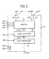
- Fig. 2 is a block diagram of one of the circuits for driving the horizontal transparent electrode lines of an embodiment of the present invention
- Fig. 3 is a block diagram of one of the circuits for driving the vertical transparent electrode lines of the embodiment of the present invention
- Fig. 4 is a construction drawing of the liquid crystal display device of the present invention.
- Fig. 4 shows the construction of the liquid crystal display device of an embodiment of the present invention.
- a front transparent substrate 2 and a back transparent substrate 2' are mounted each on both sides of liquid crystal elements 6 via sealing members 7.
- An orientational film 5 or 5' having a rubbing layer of a predetermined direction, plural lines of transparent electrodes 4 or 4' and an insulating film 3 or 3' are provided on each of the front and back transparent substrates 2 and 2' on the side facing the liquid crystal elements 6.
- a polarizing plate 1 or 1' whose polarized light absorbing axis is oriented in a specified direction is provided on the other side of each of the front and back substrates 2 and 2'.
- FIG. 1 is a block diagram showing the electrical construction of the liquid crystal display device 11 of the present invention.
- a display screen 11a comprises an effective display region A where characters and figures are visibly displayed and regions other than the effective display region or non-display regions B1, B2, ..., B6 (The entire non-display regions are hereinafter referred to by B.) where no characters and figures are displayed.
- the effective display region A contains plural lines of horizontal transparent electrodes 12a1, 12a2, ..., 12aY, 12b1, 12b2, ..., 12bY (The entire horizontal transparent electrodes are hereinafter referred to with 12.
- Y 100 so that the total number of the horizontal electrodes is 200.) and plural lines of vertical transparent electrodes 13a1, 13a2, ..., 13aX, 13b1, 13b2, ..., 13bX (The entire vertical transparent electrodes are hereinafter referred to by 13.
- X 640 so that the total number of the vertical electrodes is 1,280.) divided into an upper and lower groups and intersecting the horizontal transparent electrodes 12 to form a lattice.
- the non-display region B surrounding the effective display region A comprises six non-display regions B1 through B6 realized by at least two horizontal transparent electrodes 14a and 14b (represented by 14) and at least four vertical transparent electrodes 15a, 15b, 15c and 15d (represented by 15) divided vertically into two groups.
- the horizontal transparent electrodes 14 intersect the vertical transparent electrodes 13 and 15.
- the vertical transparent electrodes 15 intersect the horizontal transparent electrodes 12 and 14.
- the non-display region B is distinguished by oblique lines.
- Driving voltages suitable to the display state of and a desired character pattern on the display screen 11a are applied sequentially at a predetermined timing to the horizontal transparent electrodes 12 and 14 and to the vertical transparent electrodes 13 and 15 from driving means comprising a plurality of driving circuits which are later described.
- Driving circuits YD1 and YD2 (The two driving circuits are hereinafter referred to by YD.) supplying driving voltage to the plurality of the horizontal transparent electrodes 12 have 102 output terminals each.
- the total 204 output terminals are allotted with the serial reference numbers yd0 through yd101 and yd102 through yd203. (The entire output terminals are hereinafter referred to by yd.
- the output terminals yd101 and yd102 are not connected to the horizontal transparent electrodes 12.
- the lines connected to the output terminals yd are allotted with the serial reference numbers lyd0 through lyd201 (represented by lyd).
- the first output terminal yd0 and the last output terminal yd203 of the driving circuits YD are connected through the lines lyd0 and lyd201 to the horizontal transparent electrodes 14a and 14b of the non-display regions B1 and B2, respectively. All the other output terminals yd1 through yd202 (excluding the terminals yd101 and yd102) are connected via the lines lyd1 through lyd200 to the horizontal transparent electrodes 12 one to one.
- Driving circuits XD1, XD2, ..., XD2n (2n 16 in this embodiment.
- the entire driving circuits are hereinafter referred to by XD) supplying driving voltage to the plurality of the vertical transparent electrodes 13 have, say, 82 output terminals each.
- the total 1,312 output terminals are allotted with the serial reference numbers xd0 through xd1312. (The entire output terminals are hereinafter referred to by xd.
- the last output terminal xd81 of the driving circuit XD1, the first and the last output terminals xd82, xd163, xd164, xd245, xd246, xd327, ..., xd1148 and xd1229 of the subsequent driving circuits XD2 through XD15 and the first output terminal xd1230 of the driving circuit XD16 are not connected to the vertical transparent electrodes 13.)
- the lines connected to the output terminals xd are allotted with the serial reference numbers lxd0 through lxd1283 (represented by lxd).
- the first output terminal xd0 of the driving circuit XD1 and the last output terminal xd655 of the driving circuit XDn are connected through lines lxd0 and lxd641 to the vertical transparent electrodes 15a and 15b of the non-display regions B3 and B4, respectively and the first output terminal xd656 of XD9 and the last output terminal xd1312 of the driving circuit XD16 are connected through the lines lxd642 and lxd1283 to the vertical transparent electrodes 15c and 15d of the non-display regions B5 and B6, respectively.
- All the other output terminals xd1 through xd1310 (excluding the terminals xd82, xd163, xd164, xd245, xd246, xd327 xd1148, xd1229 and xd1230) are connected via the lines lxd1 through lxd1282 to the vertical transparent electrodes 13 one to one.
- driving voltages are output through the output terminals yd and xd of the driving circuits YD and XD at predetermined timings in the sequences corresponding to the desired display pattern so as to scan the display screen lla, whereby each picture element p transmits or shuts off light, that is, becomes bright or dark when driving voltage is being applied.
- the picture elements p transmit light when driving voltage is applied between the electrodes, and shut off light when driving voltage is not applied
- a normally white (or normally bright) type of display screen the picture elements p transmit light when driving voltage is not applied.
- the display screen 11a When the display screen 11a is irradiated from the back side by a light source (not shown) positioned in the rear side of perpendicularly to the paper showing Fig. 1, the desired characters or figures displayed on the screen 11a can be seen from the front side of the screen 11a. While the screen 11a is being scanned, if voltage outputs from the driving circuits XD1 through XD8 are shut off during the time of applying voltage to the horizontal electrode 14a of the non-display region B1, namely, during the period when voltage is supplied through the output terminal yd0 of the driving circuit YD1, no voltage is applied to the non-display region B1.
- the non-display region B1 becomes dark and is distinguished as a black frame.
- the non-display region B1 becomes bright so that the black frame disappears. If outputs from the driving circuits XD1 through XD8 are connected to the vertical electrodes during the above mentioned period, voltage is applied to the non-display region B1. Consequently, when the display screen 11a is of the normally black type, the non-display region B1 becomes bright so that the black frame disappears, and when the display screen 11a is of the normally white type, the non-display region B1 becomes dark, being distinguished as a black frame. All the other non-display regions B2 through B6 operate similarly as the non-display region B1.
- the liquid crystal display device of the present invention is characterized in that a plurality of horizontal transparent electrodes 14 and a plurality of vertical transparent electrodes 15 are provided even in the non-display region B of the display screen 11a, permitting voltage from the driving circuits YD and XD to be applied between the transparent electrodes 14 and 15 in the non-display region B at a predetermined timing independent of the voltage application to the transparent electrodes in the effective non-display region B.
- Fig. 2 is a block diagram showing the construction of one driving circuit YD which supplies driving voltage to the horizontal transparent electrodes of the display device of the present invention
- Fig. 3 is another block diagram showing the construction of one driving circuit XD for supplying driving voltage to the vertical transparent electrodes.
- the driving circuit YD is activated by application of supply voltage V DD and V SS .
- the driving circuit YD is provided with, say, 102 output terminals yd0 through yd101 (represented by yd).
- the driving circuits YD comprises two driving circuits YD1 and YD2.
- the output terminal yd0 of the driving circuit YD1 and the output terminal yd203 of the driving circuit YD2 are connected to the horizontal transparent electrode 14a of the non-display region B1 and to the horizontal transparent electrode 14b of the non-display region B2, respectively.
- the output terminal yd101 of the driving circuit YD1 and the output terminal yd102 of the driving circuit YD2 are not connected to the horizontal electrodes.
- the output terminals yd1 through yd100 of the driving circuit YD1 are connected to the horizontal transparent electrodes 12a1 through 12aY, and the output terminals yd103 through yd202 of the driving circuit YD2 to the horizontal transparent electrodes 12b1 through 12bY.
- the operation of the driving circuits YD is described below focusing on the driving circuit YD1.
- the driving circuit YD2 operates similarly to the driving circuit YD1.
- Driving voltage of four levels in accordance with the density of characters to be displayed on the screen is supplied from a driver Ya via line l0 through l101 to the output terminals yd (yd0 through yd101).
- the level of the driving voltage is determined by a level signal selected by the driver Ya from among four kinds of level signals supplied through level terminals vy1 through vy4 to the driver Ya while a level alternating signal supplied through a level selecting terminal dfy from a control circuit (not shown) is input to the driver Ya via a level shifter Yb and a line l201.
- Data signals are input through a data input terminal dya to a shift register Yc which outputs the data signals sequentially in shift through a line l202, for scanning or selectively driving 101 horizontal transparent electrodes (including those for the non-display region) through the output terminals yd0 through yd100.
- driving voltage is or is not supplied to the last output terminal yd101 and the first output terminal yd0 for the non-display region, depending upon the display state of the screen.
- Supposing driving voltage is being applied to the vertical transparent electrodes and that the display screen 11a is of normally black type, the non-display region becomes bright when driving voltage is supplied to the output terminals yd0 and yd101, and becomes dark when driving voltage is not supplied.
- the non-display region On the display screen 11a of normally white type, the non-display region becomes dark when driving voltage is supplied to the output terminals yd0 and yd101, and becomes bright when it is not supplied.
- driving voltage is not applied to the vertical transparent electrodes, the non-display region is dark on the normally black type screen and bright on the normally white type screen regardless of whether or not driving voltage is supplied to the output terminals yd0 and yd101.
- each driving circuit XD is activated by application of supply voltages Vdd and Vss.
- Each driving circuit XD is provided with, say, 82 output terminals xd0 through xd81 (represented by xd).
- the last output display xd81 of the driving circuit XD1 and the last output terminal xd737 of the driving circuit XD9 are not connected to the vertical transparent electrodes.
- the first and the last of the 82 output terminals of each of the driving circuits XD are either connected to the vertical transparent electrodes 15a through 15d of the non-display region B or not connected to any electrodes. All the remaining output terminals are connected to the vertical transparent electrodes in the effective display region one to one.
- the operation of the driving circuits XD is described below focusing on the driving circuit XD1.
- the other driving circuits operate similarly as the driving circuit XD1.
- the output terminals xd1 through xd80 of the driving circuit XD are connected one to one to the vertical transparent electrodes 13 of the effective display region A.
- Driving voltage of four levels in accordance with the density of characters to be displayed on the screen is supplied to the output terminals xd (xd0 through xd81) from a driver Xa via lines m0 through m81.
- the level of the driving voltage is determined by a level signal selected by the driver Xa from among four kinds of level signals supplied to the driver Xa through level terminals vx1 through vx4 while a level alternating signal supplied through a level selecting terminal dfx from a control circuit (not shown) is input to the driver Xa via a level shifter Xb and a line m201.
- Selecting data signals are input through four data input terminals dxa, dxb, dxc and dxd to a shift register Xd which outputs the signals sequentially in shift to a latch circuit Xc via a line m203, for scanning or selectively driving 80 vertical transparent electrodes 13 (excluding the one for the non-display region) through the output terminals xd1 through xd80.
- a non-display selecting data signal supplied via a non-display selecting terminal fr is input to the latch circuit Xc through lines m301 and m304 according to the display state on the screen.
- Supposing driving voltage is being applied to the non-display region B1 or B2 (through the output terminal yd0 or yd203 in Fig.
- the horizontal transparent electrode-driving circuit YD when a load signal is input to the latch circuit Xc via a load signal terminal load, the latch circuit Xc latches the non-display selecting data signal.
- the signal instructing the display of the non-display region B is transmitted through a line m202 to the level shifter Xb to the line m201 to the driver Xa, whereby driving voltage is output to all of the output terminals xd1 through xd80 or not output to any of them, depending upon the display type (normally black or normally white) of the display screen 11a.
- driving voltage is output through a line m302 or m305 to the level shifter Xb to a line m303 or m306 to the output terminal xd0 or xd81 connected to the vertical transparent electrode 15 of the non-display region.
- the driving voltage may be output or may not be output depending upon the display type (normally black or normally white) of the display screen 11a.
- driving voltage output is connected to or shut off from the electrodes in the non-display region independent of the voltage application to the effective display region for character display, whereby a black frame can be shown on the non-display region of the display screen as desired.
- the display performance of the liquid crystal display device is remarkably improved.
- the display device provides monochromatic pictures. It is possible to provide a color pictures when a color filter corresponding to the picture elements is placed on either of the two orientational films constituting the display screen.
- some of the output terminals of the driving circuits which form driving means remains unconnected to transparent electrodes.
- the driving circuits may have such a construction that all the output terminals of the driving circuits are connected to the electrodes in the effective display region. The number of required driving circuits may be decreased depending upon the number of the picture elements.
- the liquid crystal display device of the present invention contains both horizontal and vertical transparent electrodes even in the non-display region other than the effective display region of the display screen, and display means for driving each transparent electrode arranged in the non-display region independent of the other electrodes in the effective display region, so that the non-display region can be made dark or bright as desired. Namely, it is possible to show or erase a black frame on the non-display region of the screen depending upon the display state on the screen. Consequently, the use and display performance of the liquid crystal display device are improved remarkably.
Landscapes
- Physics & Mathematics (AREA)
- Engineering & Computer Science (AREA)
- General Physics & Mathematics (AREA)
- Chemical & Material Sciences (AREA)
- Crystallography & Structural Chemistry (AREA)
- Nonlinear Science (AREA)
- Computer Hardware Design (AREA)
- Theoretical Computer Science (AREA)
- Mathematical Physics (AREA)
- Optics & Photonics (AREA)
- Geometry (AREA)
- Liquid Crystal (AREA)
- Liquid Crystal Display Device Control (AREA)
- Control Of Indicators Other Than Cathode Ray Tubes (AREA)
- Devices For Indicating Variable Information By Combining Individual Elements (AREA)
Description
- The present invention relates to a liquid crystal display device.
- The conventional liquid crystal display device has a display screen comprising liquid crystal elements arranged on a plane and a pair of front and back substrates sandwiching the liquid crystal elements. On each of the front and back substrates is placed an orientational film having a rubbing layer of a predetermined direction, a transparent insulating substrate with a plurality of transparent electrodes arranged in lines thereon, and a polarizing plate with polarized light absorbing axis oriented in the predetermined direction, in this order. The front and back substrates face each other with the liquid crystal elements therebetween so that the orientational films are kept in contact with the front and back sides, respectively, of the liquid crystal elements. Generally, the lines of the transparent electrodes on the front substrate intersect the lines of the transparent electrodes on the back substrate, forming a lattice. Consequently, the display screen comprises an effective display region containing picture elements in the same quantity as the intersections M × N (M, N = the number of transparent electrode lines) between the transparent electrode lines, and a region other than the effective display region or so-called a non-display region where transparent electrodes exist on either the front or the back substrate. Normally, the effective display region is framed by the non-display region on the display screen.
- The orientational films and the polarizing plates are placed on both sides of the liquid crystal elements in such a manner that the orientation layer on one side has its orientation direction at a predetermined angle from that of the orientation layer on the other side and that the polarized light absorbing axis of the polarizing plate on one side is directed at a predetermined angle from the direction of the polarized light absorbing axis of the polarizing plate on the other side. These angles determine the display type of the screen, that is, normally black type (or normally dark type) in which the screen transmits light when voltage is being applied between the electrodes and shuts off light when voltage is not applied, or normally white type (or normally bright type) in which the screen transmits light when voltage is not applied between the electrodes and shuts off light when voltage is being applied. Either -type of the screen is employed in the conventional liquid crystal display device.
- In the display screen of the above liquid crystal display device, electrodes exist only on either side of the liquid crystal elements in the non-display region, so that driving voltage is not applied across the liquid crystal layer in the non-display region. Accordingly, when the display device is in the active state, the non-display region is either black or white depending upon the screen type. Specifically, on a normally black type screen, the non-display region is distinguished as a black frame, whereas on a normally white type screen, the non-display region is not distinguishable from the effective display region.
- US 4,412,214 describes a liquid crystal display element that includes non-display electrodes for maintaining a non-selective voltage between upper and lower non-display electrodes of the non-display area at all times.
- US 4,137,524 describes a liquid crystal display, operable in a normal display mode or a reverse printing display mode, in which a background display area is controlled according to the display mode.
- Therefore, when characters are displayed on the normally black type screen, a part of the characters may combine with the black non-display region, resulting in an illegible display of characters. When characters are to be displayed on the normally white type screen, on the other hand, it is difficult for the operator to plan the layout because of the indistinguishability of the effective display region from the non-display region, the operator is obliged to input characters without clear knowledge of the boundary of the effective region. Against this background, a liquid crystal display device whose non-display region can be made dark or bright as desired depending upon the state of the effective display region has been demanded but not yet realized.
- EP-A-0,223,309 is a prior art document under Article 54(3) EPC. This document describes a liquid crystal device for providing an edge region that does not contrast with the display portion.
- In accordance with the present invention there is provided a liquid crystal display device with a display area comprising a display region having picture elements for displaying images and a non-display region where images cannot be displayed, adjacent the display region, said device including control means for controlling both said display region and said non-display region, characterised in that said control means includes latch means arranged to supply non-display drive signals to said non-display region in accordance with a non-display selection signal provided as input to the control means for selecting the display state of said non-display region such that the display brightness of the non-display region relative to the display region can be changed independently of control of the display region.
- An advantage of the present invention is the provision of a liquid crystal display device having a display screen comprising an effective display region for showing characters and a region which surrounds the effective display region which is capable of changing display state depending upon the display state on the effective display region.
- Another advantage of the present invention is the provision of a liquid crystal display device with a display screen which is divided into an effective display region for showing characters and a non-display region where no characters are displayed, the effective display region being defined by the non-display region.
- A further advantage of the present invention is the provision of a liquid crystal display device capable of selecting the display state of a non-display region on the display screen to be in black or in white.
- Other advantages and further scope of applicability of the present invention will become apparent from the detailed description given hereinafter. It should be understood, however, that the detailed description and specific examples, while indicating preferred embodiments of the invention, are given by way of illustration only, since various changes and modifications within the scope of the invention will become apparent to those skilled in the art from this detailed description.
- According to one embodiment of the present invention, a liquid crystal display device contains a display screen comprising an effective display region in which a plurality of transparent electrodes are arranged in lines on both sides of liquid crystal elements so as to display characters and a region other than said effective display region or a non-display region where characters are not displayed; and liquid crystal driving means comprising circuits for driving the liquid crystal elements arranged in said effective display region to display desired characters, and circuits for driving the liquid crystal elements arranged in said non-display region so as to make the non-display region either dark or bright as desired.
- As described above, the liquid crystal display device of an embodiment of the present invention contains the display screen comprising the effective display region and the non-display region, and drives the liquid crystal elements in the non-display region independently of those in the effective display region, so that the non-display region can be made bright or dark as desired.
- Since it is possible to select dark or bright state for the non-display region according to the display state in the effective display region, the effective display region is distinguishable from the non-display region.
- The present invention will become more fully understood from the detailed description given hereinbelow and the accompanying drawings which are given by way of illustration only, and thus are not limitative of the present invention and wherein: Fig. 1 is a block diagram showing the electrical construction of the liquid crystal display device of an embodiment of the present invention;
Fig. 2 is a block diagram of one of the circuits for driving the horizontal transparent electrode lines of an embodiment of the present invention; Fig. 3 is a block diagram of one of the circuits for driving the vertical transparent electrode lines of the embodiment of the present invention; and Fig. 4 is a construction drawing of the liquid crystal display device of the present invention. - Fig. 4 shows the construction of the liquid crystal display device of an embodiment of the present invention.
- Referring to the Figure, a front
transparent substrate 2 and a back transparent substrate 2' are mounted each on both sides ofliquid crystal elements 6 via sealingmembers 7. Anorientational film 5 or 5' having a rubbing layer of a predetermined direction, plural lines oftransparent electrodes 4 or 4' and aninsulating film 3 or 3' are provided on each of the front and backtransparent substrates 2 and 2' on the side facing theliquid crystal elements 6. A polarizingplate 1 or 1' whose polarized light absorbing axis is oriented in a specified direction is provided on the other side of each of the front andback substrates 2 and 2'. Thetransparent electrodes 4 and 4' are arranged on the front andback substrates 2 and 2' so that they intersect each other to form a lattice with theliquid crystal elements 6 therebetween. Therefore, an effective display region comprising picture elements of the same quantity as the intersections M × N (M, N = the number of transparent electrode lines) between thetransparent electrodes 4 on thefront substrate 2 and the transparent electrodes 4' on the back substrate 2' and a display region containing either of thetransparent electrodes 4 and 4' or so-called a non-display region where no characters are displayed are formed in the display screen. On the display screen, the effective display region is surrounded by the non-display region. - In the following description of the liquid crystal display device of the present invention, it is assumed the number of transparent electrodes M on one side is 200, that the number of transparent electrodes N on the other side is 640, and that the number of picture elements in the effective display region is 200 × 640 = 128,000.
- Fig. 1 is a block diagram showing the electrical construction of the liquid
crystal display device 11 of the present invention. A display screen 11a comprises an effective display region A where characters and figures are visibly displayed and regions other than the effective display region or non-display regions B1, B2, ..., B6 (The entire non-display regions are hereinafter referred to by B.) where no characters and figures are displayed. The effective display region A contains plural lines of horizontal transparent electrodes 12a1, 12a2, ..., 12aY, 12b1, 12b2, ..., 12bY (The entire horizontal transparent electrodes are hereinafter referred to with 12. In the present embodiment, Y = 100 so that the total number of the horizontal electrodes is 200.) and plural lines of vertical transparent electrodes 13a1, 13a2, ..., 13aX, 13b1, 13b2, ..., 13bX (The entire vertical transparent electrodes are hereinafter referred to by 13. In the present embodiment, X = 640 so that the total number of the vertical electrodes is 1,280.) divided into an upper and lower groups and intersecting the horizontaltransparent electrodes 12 to form a lattice. Accordingly, (2X) × (2Y) (or 2 × 640 × 2 × 100 = 256,000 in the present invention) intersections are formed between the horizontaltransparent electrodes 12 and the vertical transparent electrodes 13, and picture elements "p" of the same number as the intersections are formed in the effective display region A. - The non-display region B surrounding the effective display region A comprises six non-display regions B1 through B6 realized by at least two horizontal
transparent electrodes 14a and 14b (represented by 14) and at least four verticaltransparent electrodes transparent electrodes 12 and 14. In the Fig. 1, the non-display region B is distinguished by oblique lines. - Driving voltages suitable to the display state of and a desired character pattern on the display screen 11a are applied sequentially at a predetermined timing to the horizontal
transparent electrodes 12 and 14 and to the vertical transparent electrodes 13 and 15 from driving means comprising a plurality of driving circuits which are later described. - Driving circuits YD1 and YD2 (The two driving circuits are hereinafter referred to by YD.) supplying driving voltage to the plurality of the horizontal
transparent electrodes 12 have 102 output terminals each. The total 204 output terminals are allotted with the serial reference numbers yd0 through yd101 and yd102 through yd203. (The entire output terminals are hereinafter referred to by yd. The output terminals yd101 and yd102 are not connected to the horizontaltransparent electrodes 12.) The lines connected to the output terminals yd are allotted with the serial reference numbers ℓyd0 through ℓyd201 (represented by ℓyd). - The first output terminal yd0 and the last output terminal yd203 of the driving circuits YD are connected through the lines ℓyd0 and ℓyd201 to the horizontal
transparent electrodes 14a and 14b of the non-display regions B1 and B2, respectively. All the other output terminals yd1 through yd202 (excluding the terminals yd101 and yd102) are connected via the lines ℓyd1 through ℓyd200 to the horizontaltransparent electrodes 12 one to one. - Driving circuits XD1, XD2, ..., XD2n (2n = 16 in this embodiment. The entire driving circuits are hereinafter referred to by XD) supplying driving voltage to the plurality of the vertical transparent electrodes 13 have, say, 82 output terminals each. The total 1,312 output terminals are allotted with the serial reference numbers xd0 through xd1312. (The entire output terminals are hereinafter referred to by xd. The last output terminal xd81 of the driving circuit XD1, the first and the last output terminals xd82, xd163, xd164, xd245, xd246, xd327, ..., xd1148 and xd1229 of the subsequent driving circuits XD2 through XD15 and the first output terminal xd1230 of the driving circuit XD16 are not connected to the vertical transparent electrodes 13.) The lines connected to the output terminals xd are allotted with the serial reference numbers ℓxd0 through ℓxd1283 (represented by ℓxd).
- The first output terminal xd0 of the driving circuit XD1 and the last output terminal xd655 of the driving circuit XDn are connected through lines ℓxd0 and ℓxd641 to the vertical
transparent electrodes transparent electrodes - In the
display device 11 of the above construction, driving voltages are output through the output terminals yd and xd of the driving circuits YD and XD at predetermined timings in the sequences corresponding to the desired display pattern so as to scan the display screen lla, whereby each picture element p transmits or shuts off light, that is, becomes bright or dark when driving voltage is being applied. Specifically, for a normally black (or normally dark) type of display screen, the picture elements p transmit light when driving voltage is applied between the electrodes, and shut off light when driving voltage is not applied, whereas for a normally white (or normally bright) type of display screen the picture elements p transmit light when driving voltage is not applied and shut off light when driving voltage is applied. - When the display screen 11a is irradiated from the back side by a light source (not shown) positioned in the rear side of perpendicularly to the paper showing Fig. 1, the desired characters or figures displayed on the screen 11a can be seen from the front side of the screen 11a. While the screen 11a is being scanned, if voltage outputs from the driving circuits XD1 through XD8 are shut off during the time of applying voltage to the horizontal electrode 14a of the non-display region B1, namely, during the period when voltage is supplied through the output terminal yd0 of the driving circuit YD1, no voltage is applied to the non-display region B1. As a result, when the display screen 11a is of the normally black type, the non-display region B1 becomes dark and is distinguished as a black frame. When the display screen 11a is of the normally white type, on the other hand, the non-display region B1 becomes bright so that the black frame disappears. If outputs from the driving circuits XD1 through XD8 are connected to the vertical electrodes during the above mentioned period, voltage is applied to the non-display region B1. Consequently, when the display screen 11a is of the normally black type, the non-display region B1 becomes bright so that the black frame disappears, and when the display screen 11a is of the normally white type, the non-display region B1 becomes dark, being distinguished as a black frame. All the other non-display regions B2 through B6 operate similarly as the non-display region B1.
- As understood from the above, the liquid crystal display device of the present invention is characterized in that a plurality of horizontal transparent electrodes 14 and a plurality of vertical transparent electrodes 15 are provided even in the non-display region B of the display screen 11a, permitting voltage from the driving circuits YD and XD to be applied between the transparent electrodes 14 and 15 in the non-display region B at a predetermined timing independent of the voltage application to the transparent electrodes in the effective non-display region B.
- Fig. 2 is a block diagram showing the construction of one driving circuit YD which supplies driving voltage to the horizontal transparent electrodes of the display device of the present invention, and Fig. 3 is another block diagram showing the construction of one driving circuit XD for supplying driving voltage to the vertical transparent electrodes.
- Referring to Fig. 2, the driving circuit YD is activated by application of supply voltage VDD and VSS. The driving circuit YD is provided with, say, 102 output terminals yd0 through yd101 (represented by yd).
- According to the present embodiment, the driving circuits YD comprises two driving circuits YD1 and YD2. The output terminal yd0 of the driving circuit YD1 and the output terminal yd203 of the driving circuit YD2 are connected to the horizontal transparent electrode 14a of the non-display region B1 and to the horizontal
transparent electrode 14b of the non-display region B2, respectively. The output terminal yd101 of the driving circuit YD1 and the output terminal yd102 of the driving circuit YD2 are not connected to the horizontal electrodes. The output terminals yd1 through yd100 of the driving circuit YD1 are connected to the horizontal transparent electrodes 12a1 through 12aY, and the output terminals yd103 through yd202 of the driving circuit YD2 to the horizontal transparent electrodes 12b1 through 12bY. The operation of the driving circuits YD is described below focusing on the driving circuit YD1. The driving circuit YD2 operates similarly to the driving circuit YD1. - Driving voltage of four levels in accordance with the density of characters to be displayed on the screen is supplied from a driver Ya via line ℓ0 through ℓ101 to the output terminals yd (yd0 through yd101). The level of the driving voltage is determined by a level signal selected by the driver Ya from among four kinds of level signals supplied through level terminals vy1 through vy4 to the driver Ya while a level alternating signal supplied through a level selecting terminal dfy from a control circuit (not shown) is input to the driver Ya via a level shifter Yb and a line ℓ201.
- Data signals are input through a data input terminal dya to a shift register Yc which outputs the data signals sequentially in shift through a line ℓ202, for scanning or selectively driving 101 horizontal transparent electrodes (including those for the non-display region) through the output terminals yd0 through yd100. During the scanning period, driving voltage is or is not supplied to the last output terminal yd101 and the first output terminal yd0 for the non-display region, depending upon the display state of the screen. Supposing driving voltage is being applied to the vertical transparent electrodes and that the display screen 11a is of normally black type, the non-display region becomes bright when driving voltage is supplied to the output terminals yd0 and yd101, and becomes dark when driving voltage is not supplied. On the display screen 11a of normally white type, the non-display region becomes dark when driving voltage is supplied to the output terminals yd0 and yd101, and becomes bright when it is not supplied. When driving voltage is not applied to the vertical transparent electrodes, the non-display region is dark on the normally black type screen and bright on the normally white type screen regardless of whether or not driving voltage is supplied to the output terminals yd0 and yd101.
- Referring to Fig. 3, each driving circuit XD is activated by application of supply voltages Vdd and Vss. Each driving circuit XD is provided with, say, 82 output terminals xd0 through xd81 (represented by xd).
- According to the present embodiment, the driving circuits XD comprises the driving circuits XD1 through XD2n=16. Of the 82 output terminals of each of the driving circuits XD, the output terminal xd0 of the driving circuit XD1, the output terminal xd655 of the driving circuit XDn=8, the output terminal xd656 of the driving circuit ZD9 and the output terminal xd1312 of the driving circuit XD2n=16 are connected to the vertical
transparent electrodes transparent electrodes 15a through 15d of the non-display region B or not connected to any electrodes. All the remaining output terminals are connected to the vertical transparent electrodes in the effective display region one to one. - The operation of the driving circuits XD is described below focusing on the driving circuit XD1. The other driving circuits operate similarly as the driving circuit XD1.
- The output terminals xd1 through xd80 of the driving circuit XD are connected one to one to the vertical transparent electrodes 13 of the effective display region A. Driving voltage of four levels in accordance with the density of characters to be displayed on the screen is supplied to the output terminals xd (xd0 through xd81) from a driver Xa via lines m0 through m81. The level of the driving voltage is determined by a level signal selected by the driver Xa from among four kinds of level signals supplied to the driver Xa through level terminals vx1 through vx4 while a level alternating signal supplied through a level selecting terminal dfx from a control circuit (not shown) is input to the driver Xa via a level shifter Xb and a line m201.
- Selecting data signals are input through four data input terminals dxa, dxb, dxc and dxd to a shift register Xd which outputs the signals sequentially in shift to a latch circuit Xc via a line m203, for scanning or selectively driving 80 vertical transparent electrodes 13 (excluding the one for the non-display region) through the output terminals xd1 through xd80. Meanwhile, a non-display selecting data signal supplied via a non-display selecting terminal fr is input to the latch circuit Xc through lines m301 and m304 according to the display state on the screen. Supposing driving voltage is being applied to the non-display region B1 or B2 (through the output terminal yd0 or yd203 in Fig. 2) by the horizontal transparent electrode-driving circuit YD, when a load signal is input to the latch circuit Xc via a load signal terminal load, the latch circuit Xc latches the non-display selecting data signal. Thus, the signal instructing the display of the non-display region B is transmitted through a line m202 to the level shifter Xb to the line m201 to the driver Xa, whereby driving voltage is output to all of the output terminals xd1 through xd80 or not output to any of them, depending upon the display type (normally black or normally white) of the display screen 11a.
- Meanwhile, driving voltage is output through a line m302 or m305 to the level shifter Xb to a line m303 or m306 to the output terminal xd0 or xd81 connected to the vertical transparent electrode 15 of the non-display region. The driving voltage may be output or may not be output depending upon the display type (normally black or normally white) of the display screen 11a.
- According to the present invention, as understood from the above, driving voltage output is connected to or shut off from the electrodes in the non-display region independent of the voltage application to the effective display region for character display, whereby a black frame can be shown on the non-display region of the display screen as desired. As a result, the display performance of the liquid crystal display device is remarkably improved.
- In the above embodiment, the display device provides monochromatic pictures. It is possible to provide a color pictures when a color filter corresponding to the picture elements is placed on either of the two orientational films constituting the display screen. The number of picture elements in the effective display region of the display screen is 2 × 640 × 200 = 256,000 in the present invention, although it is not limited to this figure. Further, in the present embodiment, some of the output terminals of the driving circuits which form driving means remains unconnected to transparent electrodes. The driving circuits may have such a construction that all the output terminals of the driving circuits are connected to the electrodes in the effective display region. The number of required driving circuits may be decreased depending upon the number of the picture elements.
- As described in the above, the liquid crystal display device of the present invention contains both horizontal and vertical transparent electrodes even in the non-display region other than the effective display region of the display screen, and display means for driving each transparent electrode arranged in the non-display region independent of the other electrodes in the effective display region, so that the non-display region can be made dark or bright as desired. Namely, it is possible to show or erase a black frame on the non-display region of the screen depending upon the display state on the screen.
Consequently, the use and display performance of the liquid crystal display device are improved remarkably.
Claims (6)
- A liquid crystal display device with a display area (lla) comprising a display region (A) having picture elements for displaying images and a non-display region (B1 to B6), where images cannot be displayed, adjacent the display region, said device including control means (XD, YD) for controlling both said display region and said non-display region, characterised in that said control means includes latch means (Xc) arranged to supply non-display drive signals to said non-display region in accordance with a non-display selection signal provided as input to the control means for selecting the display state of said non-display region such that the display brightness of the non-display region relative to the display region can be changed independently of control of the display region.
- A liquid crystal device according to claim 1 wherein the display area (11a) has a plurality of display control electrodes (12, 13, 14, 15) and wherein the control means includes display driver circuit means (XD, YD) which comprises a row of separate driving circuits formed in individual circuit units (XD1 to XD16), and a column of separate driving circuits formed in individual circuit units (YD1 and YD2) disposed peripherally of said display area (11a), said driving circuits being connected to said display control electrodes (12, 13, 14, 15).
- A liquid crystal device according to claim 2 wherein the display area (11a) has a plurality of non-display electrodes (14a, 14b, 15a to 15d) controlling said non-display region, and wherein each said driving circuit has a line of output terminals (e.g. xd0 to xd81) including a non-display output terminal (e.g. xd0 xd81) wherein each said non-display electrode is connected to a respective proximate non-display output terminal.
- A liquid crystal device according to claim 3 wherein the non-display electrodes (14a, 14b, 15a to 15d) define said non-display region (B1 to B6) as a peripheral region which surrounds said display region (A), and wherein the non-display output terminals to which the non-display electrodes are connected each belong to a driving circuit (YD1, YD2, XD1, XD8, XD9, XD16) disposed at an end of said column (YD1, YD2) or row (XD1 to XD8, XD9 to XD16) of said driving circuits.
- A liquid crystal display device according to claim 1, wherein said display area (11a) includes a set of display control electrodes (13, 15), said set comprising display electrodes (13a1 to 13ax or 13b1 to 13bx) for controlling display in said display region (A) and non-display electrodes (15a, 15b or 15c, 15d) for controlling the display state in said non-display region (B3, B4 or B5, B6), and wherein said control means includes display driver circuit means (XD1 to XD8 or XD9 to XD16) having display control terminals (xd1 to xd80 etc, xd574 to xd654 or xd657 to xd736 etc, xd1231 to xd1311) connected to said display electrodes, and non-display control terminals (xd0, xd655 or xd656, xd1312) connected to said non-display electrodes, shift register means (Xd) for receiving display signals and for providing display drive signals to be supplied to said display control terminals, and signal level shift means (Xb) for altering the level of the display drive signals, said latch means (Xc) being arranged to supply the non-display drive signals to said non-display control terminals.
- A liquid crystal display device according to claim 5 wherein said latch means (Xc) is responsive to a load signal (load) generated at a time when a further non-display electrode (14a or 14b) of said display area (11a) receives a non-display drive signal, said further non-display electrode extending across said set of display control electrodes, so as to latch all of the display drive signals in accordance with said non-display selection signal so that at said time said set of display control electrodes are all driven identically to produce the selected brightness in the part of the non-display region (B1 or B2) defined by said further non-display electrode.
Applications Claiming Priority (2)
| Application Number | Priority Date | Filing Date | Title |
|---|---|---|---|
| JP59183/87 | 1987-03-14 | ||
| JP62059183A JPS63225295A (en) | 1987-03-14 | 1987-03-14 | Liquid crystal display device |
Publications (3)
| Publication Number | Publication Date |
|---|---|
| EP0283235A2 EP0283235A2 (en) | 1988-09-21 |
| EP0283235A3 EP0283235A3 (en) | 1990-05-23 |
| EP0283235B1 true EP0283235B1 (en) | 1997-05-28 |
Family
ID=13106037
Family Applications (1)
| Application Number | Title | Priority Date | Filing Date |
|---|---|---|---|
| EP88302226A Expired - Lifetime EP0283235B1 (en) | 1987-03-14 | 1988-03-14 | Liquid crystal display device |
Country Status (4)
| Country | Link |
|---|---|
| US (1) | US4824212A (en) |
| EP (1) | EP0283235B1 (en) |
| JP (1) | JPS63225295A (en) |
| DE (1) | DE3855923T2 (en) |
Families Citing this family (36)
| Publication number | Priority date | Publication date | Assignee | Title |
|---|---|---|---|---|
| US4965563A (en) * | 1987-09-30 | 1990-10-23 | Hitachi, Ltd. | Flat display driving circuit for a display containing margins |
| JP2651204B2 (en) * | 1988-07-14 | 1997-09-10 | キヤノン株式会社 | Driving method of liquid crystal device |
| US5299039A (en) * | 1988-07-21 | 1994-03-29 | Proxima Corporation | Stacked display panel construction and method of aligning pixel elements thereof |
| US5233447A (en) * | 1988-10-26 | 1993-08-03 | Canon Kabushiki Kaisha | Liquid crystal apparatus and display system |
| JPH02117590U (en) * | 1989-03-07 | 1990-09-20 | ||
| US7212181B1 (en) | 1989-03-20 | 2007-05-01 | Hitachi, Ltd. | Multi-tone display device |
| JPH02245793A (en) | 1989-03-20 | 1990-10-01 | Hitachi Ltd | matrix display device |
| FR2657987B1 (en) * | 1990-02-06 | 1992-04-10 | Commissariat Energie Atomique | METHOD FOR CONTROLLING A MATRIX SCREEN COMPRISING TWO INDEPENDENT PARTS AND DEVICE FOR ITS IMPLEMENTATION. |
| EP0476797B1 (en) * | 1990-09-21 | 1996-04-24 | Sharp Kabushiki Kaisha | Liquid crystal display device |
| JPH04223429A (en) * | 1990-12-26 | 1992-08-13 | Canon Inc | display device |
| JPH0591447A (en) * | 1991-09-25 | 1993-04-09 | Toshiba Corp | Transmissive liquid crystal display device |
| JP2894039B2 (en) * | 1991-10-08 | 1999-05-24 | 日本電気株式会社 | Display device |
| JPH05241127A (en) * | 1992-02-28 | 1993-09-21 | Canon Inc | Liquid crystal display device |
| JPH07504997A (en) * | 1992-03-20 | 1995-06-01 | ブイ エル エス アイ テクノロジー,インコーポレイテッド | VGA controller and driving method using address conversion for driving dual scan LCD panel |
| US5299043A (en) * | 1993-02-23 | 1994-03-29 | Merlin Industries | Underwater liquid crystal display apparatus having identical polarizers and reflector in both the matting and liquid crystal cell |
| JP3310082B2 (en) * | 1993-12-24 | 2002-07-29 | シャープ株式会社 | Liquid crystal display device and coordinate detection method in liquid crystal integrated tablet |
| JP3454971B2 (en) | 1995-04-27 | 2003-10-06 | 株式会社半導体エネルギー研究所 | Image display device |
| US5724063A (en) * | 1995-06-07 | 1998-03-03 | Seiko Epson Corporation | Computer system with dual-panel LCD display |
| JPH09101503A (en) * | 1995-10-04 | 1997-04-15 | Semiconductor Energy Lab Co Ltd | Display device |
| TW440742B (en) * | 1997-03-03 | 2001-06-16 | Toshiba Corp | Flat panel display device |
| FR2784489B1 (en) * | 1998-10-13 | 2000-11-24 | Thomson Multimedia Sa | METHOD FOR DISPLAYING DATA ON A MATRIX DISPLAY |
| US7425970B1 (en) | 2000-11-08 | 2008-09-16 | Palm, Inc. | Controllable pixel border for a negative mode passive matrix display device |
| US7724270B1 (en) | 2000-11-08 | 2010-05-25 | Palm, Inc. | Apparatus and methods to achieve a variable color pixel border on a negative mode screen with a passive matrix drive |
| US6961029B1 (en) | 2000-11-08 | 2005-11-01 | Palm, Inc. | Pixel border for improved viewability of a display device |
| JP3951042B2 (en) * | 2001-03-09 | 2007-08-01 | セイコーエプソン株式会社 | Display element driving method and electronic apparatus using the driving method |
| US7126588B2 (en) * | 2002-06-27 | 2006-10-24 | Intel Corporation | Multiple mode display apparatus |
| JP4633538B2 (en) * | 2005-05-23 | 2011-02-16 | 三菱電機株式会社 | Image display device and large image display device |
| GB0702350D0 (en) | 2007-02-07 | 2007-03-21 | Plastic Logic Ltd | Electronic reading devices |
| GB0702347D0 (en) | 2007-02-07 | 2007-03-21 | Plastic Logic Ltd | Electronic document reading devices |
| GB0702349D0 (en) | 2007-02-07 | 2007-03-21 | Plastic Logic Ltd | Electronic document readers and reading devices |
| GB2454033A (en) | 2007-10-24 | 2009-04-29 | Plastic Logic Ltd | Portable paperless electronic printer |
| GB2458106B (en) | 2008-03-03 | 2012-07-18 | Plastic Logic Ltd | Electronic document reader system |
| GB2463266B (en) | 2008-09-05 | 2011-07-27 | Plastic Logic Ltd | Electronic document reader |
| GB201000021D0 (en) | 2010-01-04 | 2010-02-17 | Plastic Logic Ltd | Electronic document reading devices |
| KR101996655B1 (en) * | 2012-12-26 | 2019-07-05 | 엘지디스플레이 주식회사 | apparatus for displaying a hologram |
| US20150277506A1 (en) | 2014-03-29 | 2015-10-01 | Bok Eng Cheah | Micro-hinge for an electronic device |
Family Cites Families (12)
| Publication number | Priority date | Publication date | Assignee | Title |
|---|---|---|---|---|
| US4137524A (en) * | 1977-09-28 | 1979-01-30 | Optel Corporation | Reversible printing display |
| US4224617A (en) * | 1978-08-23 | 1980-09-23 | General Electric Company | Liquid crystal display |
| US4277786A (en) * | 1979-07-19 | 1981-07-07 | General Electric Company | Multi-electrode liquid crystal displays |
| US4443062A (en) * | 1979-09-18 | 1984-04-17 | Citizen Watch Company Limited | Multi-layer display device with nonactive display element groups |
| JPS576882A (en) * | 1980-06-16 | 1982-01-13 | Hitachi Ltd | Liquid crystal display element |
| JPS58216289A (en) * | 1982-06-10 | 1983-12-15 | シャープ株式会社 | Liquid crystal display driving circuit |
| JPS58220176A (en) * | 1982-06-17 | 1983-12-21 | シャープ株式会社 | Liquid crystal display |
| JPH0654960B2 (en) * | 1983-10-20 | 1994-07-20 | シチズン時計株式会社 | Driving method for liquid crystal display device |
| JPS61124990A (en) * | 1984-11-22 | 1986-06-12 | 沖電気工業株式会社 | Lcd matrix panel driving circuit |
| JPH0766248B2 (en) * | 1985-02-04 | 1995-07-19 | 株式会社日立製作所 | Liquid crystal display device and driving method thereof |
| NL8503180A (en) * | 1985-11-19 | 1987-06-16 | Philips Nv | DISPLAY DEVICE. |
| FR2596187B1 (en) * | 1986-03-18 | 1988-05-13 | Commissariat Energie Atomique | METHOD FOR SEQUENTIALLY CONTROLLING A LIQUID CRYSTAL MATRIX DISPLAY HAVING DIFFERENT OPTICAL RESPONSES IN ALTERNATIVE AND CONTINUOUS FIELDS |
-
1987
- 1987-03-14 JP JP62059183A patent/JPS63225295A/en active Pending
-
1988
- 1988-03-14 DE DE3855923T patent/DE3855923T2/en not_active Expired - Fee Related
- 1988-03-14 US US07/167,889 patent/US4824212A/en not_active Expired - Lifetime
- 1988-03-14 EP EP88302226A patent/EP0283235B1/en not_active Expired - Lifetime
Also Published As
| Publication number | Publication date |
|---|---|
| DE3855923D1 (en) | 1997-07-03 |
| EP0283235A2 (en) | 1988-09-21 |
| DE3855923T2 (en) | 1997-12-18 |
| US4824212A (en) | 1989-04-25 |
| EP0283235A3 (en) | 1990-05-23 |
| JPS63225295A (en) | 1988-09-20 |
Similar Documents
| Publication | Publication Date | Title |
|---|---|---|
| US4824212A (en) | Liquid crystal display device having separate driving circuits for display and non-display regions | |
| EP1361505B1 (en) | Liquid crystal display device with two screens and driving method of the same | |
| JP4191408B2 (en) | Liquid crystal display | |
| EP0848369B1 (en) | Light Modulating devices with addressable matrix of elements and greyscale levels by spatial and/or temporal dithering wherein one or more subelements and/or one or more subframes can be set to more than two different light transmission states | |
| JP4490708B2 (en) | Display device | |
| JPH1010546A (en) | Display device and its driving method | |
| KR960704428A (en) | Display device | |
| JPH022585A (en) | Pixel array having zig-zag three primary color | |
| EP0347187B1 (en) | Color display panel | |
| EP0860808A2 (en) | Matrix display with an additional icon row | |
| US4743896A (en) | Electrode pattern for a liquid crystal display | |
| EP0830666B1 (en) | Plasma-addressed display | |
| US7199775B2 (en) | Display device array substrate and display device | |
| US4384763A (en) | Double layer liquid crystal device for a dot matrix display | |
| WO2000016305A1 (en) | Matrix display device | |
| JP2001264823A (en) | Electrochromic display device | |
| US20010035851A1 (en) | Liquid crystal display apparatus | |
| CN220731152U (en) | Electronic paper display device, display panel and display device | |
| KR100730270B1 (en) | Liquid crystal display device | |
| JPH0614154B2 (en) | LCD matrix panel | |
| JPH0315752B2 (en) | ||
| CN117037721A (en) | Electronic paper display device, display panel and display device | |
| JP2004037905A (en) | Liquid crystal display device | |
| KR100654217B1 (en) | LCD panel and liquid crystal display device having same | |
| KR100694656B1 (en) | Display unit for liquid crystal display |
Legal Events
| Date | Code | Title | Description |
|---|---|---|---|
| PUAI | Public reference made under article 153(3) epc to a published international application that has entered the european phase |
Free format text: ORIGINAL CODE: 0009012 |
|
| AK | Designated contracting states |
Kind code of ref document: A2 Designated state(s): DE GB |
|
| PUAL | Search report despatched |
Free format text: ORIGINAL CODE: 0009013 |
|
| AK | Designated contracting states |
Kind code of ref document: A3 Designated state(s): DE GB |
|
| 17P | Request for examination filed |
Effective date: 19901113 |
|
| 17Q | First examination report despatched |
Effective date: 19921214 |
|
| GRAG | Despatch of communication of intention to grant |
Free format text: ORIGINAL CODE: EPIDOS AGRA |
|
| GRAH | Despatch of communication of intention to grant a patent |
Free format text: ORIGINAL CODE: EPIDOS IGRA |
|
| GRAH | Despatch of communication of intention to grant a patent |
Free format text: ORIGINAL CODE: EPIDOS IGRA |
|
| GRAA | (expected) grant |
Free format text: ORIGINAL CODE: 0009210 |
|
| AK | Designated contracting states |
Kind code of ref document: B1 Designated state(s): DE GB |
|
| REF | Corresponds to: |
Ref document number: 3855923 Country of ref document: DE Date of ref document: 19970703 |
|
| PLBE | No opposition filed within time limit |
Free format text: ORIGINAL CODE: 0009261 |
|
| STAA | Information on the status of an ep patent application or granted ep patent |
Free format text: STATUS: NO OPPOSITION FILED WITHIN TIME LIMIT |
|
| 26N | No opposition filed | ||
| REG | Reference to a national code |
Ref country code: GB Ref legal event code: IF02 |
|
| PGFP | Annual fee paid to national office [announced via postgrant information from national office to epo] |
Ref country code: GB Payment date: 20020313 Year of fee payment: 15 |
|
| PGFP | Annual fee paid to national office [announced via postgrant information from national office to epo] |
Ref country code: DE Payment date: 20020327 Year of fee payment: 15 |
|
| PG25 | Lapsed in a contracting state [announced via postgrant information from national office to epo] |
Ref country code: GB Free format text: LAPSE BECAUSE OF NON-PAYMENT OF DUE FEES Effective date: 20030314 |
|
| PG25 | Lapsed in a contracting state [announced via postgrant information from national office to epo] |
Ref country code: DE Free format text: LAPSE BECAUSE OF NON-PAYMENT OF DUE FEES Effective date: 20031001 |
|
| GBPC | Gb: european patent ceased through non-payment of renewal fee |
Effective date: 20030314 |