EP0282528B1 - Nonvolatile memory cell - Google Patents
Nonvolatile memory cell Download PDFInfo
- Publication number
- EP0282528B1 EP0282528B1 EP87905897A EP87905897A EP0282528B1 EP 0282528 B1 EP0282528 B1 EP 0282528B1 EP 87905897 A EP87905897 A EP 87905897A EP 87905897 A EP87905897 A EP 87905897A EP 0282528 B1 EP0282528 B1 EP 0282528B1
- Authority
- EP
- European Patent Office
- Prior art keywords
- floating gate
- nonvolatile memory
- memory cell
- electrode
- program
- Prior art date
- Legal status (The legal status is an assumption and is not a legal conclusion. Google has not performed a legal analysis and makes no representation as to the accuracy of the status listed.)
- Expired - Lifetime
Links
- 238000007667 floating Methods 0.000 claims abstract description 57
- 229910021420 polycrystalline silicon Inorganic materials 0.000 claims abstract description 12
- 229920005591 polysilicon Polymers 0.000 claims abstract description 12
- 230000008878 coupling Effects 0.000 claims description 16
- 238000010168 coupling process Methods 0.000 claims description 16
- 238000005859 coupling reaction Methods 0.000 claims description 16
- 239000000758 substrate Substances 0.000 claims description 14
- 239000003989 dielectric material Substances 0.000 claims description 9
- 239000004065 semiconductor Substances 0.000 claims description 9
- 229910052710 silicon Inorganic materials 0.000 claims description 4
- 239000010703 silicon Substances 0.000 claims description 4
- 150000004767 nitrides Chemical class 0.000 claims description 2
- 230000000295 complement effect Effects 0.000 abstract description 14
- 238000004519 manufacturing process Methods 0.000 abstract description 6
- 230000008901 benefit Effects 0.000 abstract description 3
- 238000009792 diffusion process Methods 0.000 description 13
- 230000005669 field effect Effects 0.000 description 11
- 239000003990 capacitor Substances 0.000 description 9
- 238000012360 testing method Methods 0.000 description 6
- 238000012546 transfer Methods 0.000 description 6
- 230000005641 tunneling Effects 0.000 description 4
- VYPSYNLAJGMNEJ-UHFFFAOYSA-N Silicium dioxide Chemical class O=[Si]=O VYPSYNLAJGMNEJ-UHFFFAOYSA-N 0.000 description 3
- XUIMIQQOPSSXEZ-UHFFFAOYSA-N Silicon Chemical compound [Si] XUIMIQQOPSSXEZ-UHFFFAOYSA-N 0.000 description 3
- 238000013461 design Methods 0.000 description 3
- 238000000034 method Methods 0.000 description 3
- 238000003491 array Methods 0.000 description 2
- 238000001514 detection method Methods 0.000 description 2
- 230000006870 function Effects 0.000 description 2
- 230000014759 maintenance of location Effects 0.000 description 2
- 230000008569 process Effects 0.000 description 2
- 235000012239 silicon dioxide Nutrition 0.000 description 2
- 230000005689 Fowler Nordheim tunneling Effects 0.000 description 1
- 229910052581 Si3N4 Inorganic materials 0.000 description 1
- 238000013459 approach Methods 0.000 description 1
- 230000009286 beneficial effect Effects 0.000 description 1
- 230000036755 cellular response Effects 0.000 description 1
- 239000002131 composite material Substances 0.000 description 1
- 238000013524 data verification Methods 0.000 description 1
- 230000001934 delay Effects 0.000 description 1
- 230000005684 electric field Effects 0.000 description 1
- 238000005516 engineering process Methods 0.000 description 1
- 238000002347 injection Methods 0.000 description 1
- 239000007924 injection Substances 0.000 description 1
- 238000005192 partition Methods 0.000 description 1
- 238000012545 processing Methods 0.000 description 1
- 230000008672 reprogramming Effects 0.000 description 1
- 239000000377 silicon dioxide Substances 0.000 description 1
- HQVNEWCFYHHQES-UHFFFAOYSA-N silicon nitride Chemical compound N12[Si]34N5[Si]62N3[Si]51N64 HQVNEWCFYHHQES-UHFFFAOYSA-N 0.000 description 1
- 230000003068 static effect Effects 0.000 description 1
- 230000001052 transient effect Effects 0.000 description 1
Images

Classifications
-
- G—PHYSICS
- G11—INFORMATION STORAGE
- G11C—STATIC STORES
- G11C14/00—Digital stores characterised by arrangements of cells having volatile and non-volatile storage properties for back-up when the power is down
-
- G—PHYSICS
- G11—INFORMATION STORAGE
- G11C—STATIC STORES
- G11C16/00—Erasable programmable read-only memories
- G11C16/02—Erasable programmable read-only memories electrically programmable
- G11C16/04—Erasable programmable read-only memories electrically programmable using variable threshold transistors, e.g. FAMOS
- G11C16/0408—Erasable programmable read-only memories electrically programmable using variable threshold transistors, e.g. FAMOS comprising cells containing floating gate transistors
- G11C16/0441—Erasable programmable read-only memories electrically programmable using variable threshold transistors, e.g. FAMOS comprising cells containing floating gate transistors comprising cells containing multiple floating gate devices, e.g. separate read-and-write FAMOS transistors with connected floating gates
Definitions
- This invention relates to nonvolatile memory cells as indicated in the preamble of claim 1 and as e.g. known from WO-A- 85/03798.
- Integrated circuit nonvolatile memory cells which store binary data (0 or 1) for extended periods of time are generally well-known.
- Contemporary and representative designs involve the use of MNOS or floating gate structures which are programmed by the tunneling of charge through dielectrics, the conduction of charge through dielectrics, or the injection of high energy electrons through dielectrics under the influence of electric fields.
- the cell designs were primarily influenced by the continuing pursuit of smaller dimensions with the intent of maximizing the density of nonvolatile memory arrays and minimizing chip size.
- a nonvolatile memory cell is known from IEEE Journal of Solid-State Circuits, Vol. SC-20, No. 2, April 1985, pages 603-608, R. Cuppens et al: "An EEPROM for Microprocessors and Custom Logic'.
- the known nonvolatile memory cell includes a transistor having a polysilicon floating gate which has a relatively large capacitive coupling between the floating gate and a control gate and a relatively small capacitive coupling between the floating gate and the transistor drain region.
- the control gate is formed by a diffusion region in the semiconductor substrate.
- the known nonvolatile memory cell has the advantage that only a single polysilicon layer is utilized in the manufacture of the cell. However, the cell has the disadvantage that the readout speed is slow.
- a bistable latch circuit including first and second field effect transistors disposed in respective first and second branches.
- the respective gate electrode of each transistor is cross-coupled to the respective drain of the other transistor.
- First and second floating gate transistors each having a control gate and an insulated floating gate, are respectively disposed in the first and second circuit branches.
- Each floating gate is capacitively coupled to a doped substrate region which is connected to a programming node connected to the control gate of the other floating gate transistor.
- a programming circuit applies high and low potentials to the programming nodes.
- the floating gates of the respective floating gate transistors are thereby charged differentially to cause the floating gate transistors to be operative in respective enhancement and depletion modes during subsequent read operations.
- Nonvolatile RAM cell in the form of a six-transistor latch in which the N-channel devices include floating polysilicon gates. Each floating gate is capacitively coupled to the drain of the associated transistor. The control gate of each floating gate transistor is cross-coupled to the drain connection of the other floating gate transistor. When power is removed and reapplied, the cell will power up with the complement of the memory state that existed during the nonvolatile write.
- first and second bit lines serving as readout lines enables a sense amplifier connected to said first and second bit lines to be differentially driven, whereby a high sensing speed is attainable.
- Fig. 1 is a schematic embodiment of a high speed direct write differential nonvolatile memory cell.
- Fig. 2 is an embodying layout for a high speed direct write differential nonvolatile memory cell.
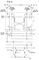
- Fig. 3 is a schematic illustrating the placement of a high speed nonvolatile memory cell within an array having a differential nonvolatile data sensing means.
- the present invention is illustrated by the embodiment schematically depicted in Fig. 1 of the drawings.
- the high speed, direct write differential nonvolatile memory cell 1 uses as a row select common word line 2, which line ohmically connects the gate electrodes of cell access field effect transistors (FETs) 3, 4, 6 and 7.
- FETs cell access field effect transistors
- Floating gate sense FETs 8 and 9 are connected in electrical series with cell access transistors 3 and 7, respectively, and are individually responsive to the charge held on respective floating gate electrodes 11 and 12.
- the polarity of the charge transferred onto floating gate electrodes 11 and 12 is inherently complementary, to conductively bias one of the floating gate sense transistors 8 or 9 at a substantially higher level than the differentially situated complement.
- An addressing of cell access field effect transistors 3 and 7 by a select signal on word line 2 enables the conductive states of floating gate sense transistors 8 and 9 to be sensed on bit lines number one and number two using a high speed sense amplifier.
- the nonvolatile data state stored in memory cell 1 is read out at relatively high speed because the sense amplifier connected to bit lines number one and number two is differentially driven, in contrast to a reference level responsive sense amplifier which must await a bit line charge decay to detect the cell data.
- Floating gate electrodes 11 and 12 of cell 1 are capacitively cross-coupled to source/drain diffusion electrode regions 13 and 14 of field effect transistors 4 and 6.
- floating gate electrode 11 is coupled by relatively small capacitor C3 to source/drain electrode region 13, and by relatively large capacitor C2 to complementary operable source/drain electrode region 14.
- floating gate electrode 12 is coupled through relatively small capacitor C4 to source/drain electrode region 14 and by relatively large capacitor C1 to source/drain electrode region 13.
- Electrode regions 13 and 14 are separated from complementary operable program lines number one (reference numeral 22) and number two (reference numeral 23) by respective cell access FETs 4 and 6, which as noted earlier are responsive to the signal on word line 2.
- the circuit symmetry conveyed by the schematic in Fig. 1 is more vividly apparent upon considering a representative layout of high speed direct write differential nonvolatile memory cell 1, as depicted in Fig. 2.
- the layout in Fig. 2 depicts one representative cell from an array configuration composed of multiple nonvolatile memory cells, fabricated as an integrated circuit using a silicon semiconductor substrate and contemporary single polysilicon manufacturing techniques.
- complementary bit lines number one and number two referenced as n+ doped diffused regions 16 and 17, are connected through cell access field effect transistors 3 and 7 to further n+ diffusions 18 and 19 in the p ⁇ doped silicon substrate.
- this is implemented using p-wells in an n-type substrate.
- Floating gate sense transistors 8 and 9 are interposed respectively between diffused regions 18 and 19 and common control electrode 21. Together these patterns define commonly addressed parallel bit line paths on opposite sides of the cell.
- the interior structure of the cell is comprised of program lines number one and number two, referenced as n+ diffusions 22 and 23, which upon passing through corresponding cell access field effect transistors 4 and 6 continue as conductive diffusion regions 13 and 14.
- Substrate diffusions 13 and 14 project in parallel through the cell interior, generally defined by dielectric fabrication mask pattern 27.
- word line electrode 2 and floating gate electrodes 11 and 12 are formed from a conductively doped polysilicon layer, following selective processing to create the FET gate silicon dioxides (oxides) and the thin capacitor and charge transfer oxides.
- field effect transistors 3, 4, 6, 7, 8 and 9 utilize a gate oxide approximately 40 nanometers thick, while the thin oxide dielectric layers in regions C1-C4 have a nominal thickness of 9 nanometers, the latter selected to match the needs of both capacitive coupling and charge transfer.
- polysilicon floating gate electrode 11 overlaps diffused electrode 13 in a relatively small area, to create a comparatively small capacitive coupling C3, and overlaps diffused electrode 14 in a relatively large area, to form a comparatively large capacitive coupling C2.
- Polysilicon floating gate electrode 12 has a complementary arrangement to that of electrode 11, in that electrode 12 overlaps diffusion 14 to form a relatively small capacitive coupling C4 and then extends over diffusion 13 to form a relatively large capacitive coupling C1.
- the magnitudes of the capacitors C1-C4 are defined in conventional manner by the areas of overlap and the thicknesses of the respective thin dielectric layers.
- the movement of the charge to and from floating gate electrodes 11 and 12 occurs in capacitive coupling regions C3 and C4 of the respective electrodes.
- the thin dielectric in these regions is preferably composed of thermally grown silicon dioxide, so that charge transfer occurs in the regions C3 and C4 by Fowler-Nordheim tunneling. If, in the alternative, the thin dielectrics are composed of a silicon nitride dielectric layer, or a thin silicon oxynitride composite dielectric layer, charge transfer would occur by Poole-Frenkel conduction or a combination of such conduction with tunneling.
- the choice of the dielectric material for regions C1-C4 is influenced by a number of factors not central to this invention, such as capacitor area requirements, dielectric coefficients, cell retention requirements and cell endurance characteristics, which relationships are commonly known and considered by practitioners in the art.
- Table A summarizes the operating conditions suitable for the direct writing of the exemplary high speed nonvolatile memory cell depicted in the Figs. 1 and 2.
- differential nonvolatile memory cell 1 to retain a binary "0" state is accomplished by providing a +5 volt select signal to word line 2; providing a +5 volt signal to the program line number one, connection 22; and providing a -9 volt signal to program line number two, connection 23, both bit lines, the p-well and common control electrode 21.
- transistors 4 and 6 are conductive so as to pass approximately +3 volts to diffusion 13 and -9 volts to diffusion 14. Because capacitive coupling C1 is significantly larger than C4, floating gate electrode 12 is pulled to +3 volts via capacitor C1.
- nonvolatile memory cell 1 is fabricated with n-channel field effect transistors in a p-well CMOS process.
- the features of the cell are, however, not so limited in that they are equally amendable to other CMOS, NMOS or PMOS implementations.
- a particularly noteworthy feature evidenced by the foregoing description of a program/write cycle is the provision of a complementary nonvolatile write without a preceding erase operation, which erase cycle characterizes most conventional nonvolatile memory cells.
- This direct write capability minimizes the time associated with the programming/writing of a nonvolatile state into each cell, which time for this embodiment entails approximately 10 milliseconds.
- the binary bit stored in nonvolatile cell 1 is detected by sensing the relative conductive states of the paths defined between bit lines number one and number two, and common control electrode 21, having interposed therebetween respective cell access FETs 3 and 7 and floating gate sense FETs 8 and 9.
- the reading of the data state in the cell involves the concurrent application of +5 volts to word line 2, to program line number one and to program line number two, and a detection of the relative conductive difference in the bit lines number one and number two.
- the intrinsic threshold voltage of floating gate sense transistors 8 and 9 is approximately 1 volt.
- the complementary pair of sense FETs have thresholds of approximately +4 and -2 volts.
- the threshold voltage difference is reflected in conduction current differential for bit lines number one and number two.
- Differential conduction of floating gate sense transistors 8 and 9, relating to the voltage differential charge on floating gate electrodes 11 and 12, can be detected on bit lines number one and number two using a differential responsive sense amplifier, such as amplifier 33 as embodied in the cell array circuit of Fig. 3.
- bit lines number one and number two are pull-up biased through load connected field effect transistors 28 and 29, and are coupled by way of column select field effect transistors 31 and 32 to the opposite sides of voltage responsive sense amplifier 33.
- the binary state stored in nonvolatile memory cell 1 is represented by the voltage on data out line 34.
- the differential character of the present cell consumes somewhat greater chip area, and consequently reduces function density, in comparison to that attainable using a non-differential configuration.
- the differential arrangement provides a nonvolatile cell with distinctly superior readout speed.
- the output state of the present cell can be detected almost immediately, in that sensing is differentially responsive.
- the delays associated with transient decays when comparing to a fixed reference voltage are obviated. Futhermore, the differential configuration effectively doubles the memory cell window, which window margin is used by differential detection to accentuate speed.
- the voltages shown by parentheses in Table A represent alternate arrangements.
- the +5 volt bias voltages coupled floating gate electrodes 11 and 12 from program lines number one and number two during the read operation are preferred but not mandatory conditions.
- Such biasing of the two floating gate electrodes by +5 volts during reading will shift the operating ranges of floating gate sense transistors 8 and 9 to regions of higher gain, so as to further accentuate the effective difference represented by the complementary charged states of the two floating gate electrodes.
- the high speed direct write differential nonvolatile memory cell of the present invention also provides the user with a memory margining capability, which capability is suitable for product acceptance testing or for data verification.
- the margining conditions are also set forth in Table A.
- bit lines number one and number two are connected to the sense amplifier while the test voltages are applied individually through the program lines.
- memory margining is done with positive voltages. This avoids the need for negatively biasing the substrate or p-well to prevent inadvertent forward biasing of pn junctions.
- the differential operation of the cell facilitates memory margin testing by virtue of the symmetry of structure and operation.
- test voltage used to bias the selected program line causes a cell response which is indicative of a threshold voltage difference between the two floating gate sense transistors, rather than an absolute voltage
- multiple cells in an array can first be programmed to a data "0" state and tested using one program line for margining, followed by a reprogramming to the opposite "1" state and similar margining using one other program line. Thereby, both the "0" and "1" states are measured while avoiding the use of negative voltages.
- This margining approach can also be used to evaluate the performance of a memory cell after an extended period of time following a program/write cycle. For example, the sensing of thresholds via one and then the other of the program lines can be used to test retention or to "peek" at the state of the memory cell in actual use. However, it should recognize that "peeking" will subject the cell to limited programming conditions by virtue of the voltages impressed across the charge transfer dielectrics.
- direct write differential nonvolatile memory cell 1 is by virtue of its functional and structural symmetry very suitable for implementation in arrays. In such applications it is foreseeable that the benefits of the high operating speed, the structural and functional symmetry, and the single polysilicon fabrication capability will lead to applications beyond semicustom integrated circuit products. In considering such broader, array type applications, another beneficial aspect of the cell may be exercised. When suitable for the array as a whole, cell access transistors 4 and 6 may be operationally grouped by commonly connecting gate electrodes of multiple cells to provide a block programming capability.
- the direct write differential nonvolatile memory cell configuration described herein thereby provides not only accentuated read rate capability for an EEPROM cell, but also exhibits a direct write capability, memory window margining capability, symmetry as to both structure and functions, and amenability to being fabricated using a relatively conventional single polysilicon process technology. Furthermore, the cell is configured to allow the partition of the relatively high programming voltage, so that individual transistor voltages are limited to magnitudes which can be handled by very large scale integrated field effect devices of conventional and advanced design.
Landscapes
- Engineering & Computer Science (AREA)
- Microelectronics & Electronic Packaging (AREA)
- Read Only Memory (AREA)
Abstract
Description
- This invention relates to nonvolatile memory cells as indicated in the preamble of claim 1 and as e.g. known from WO-A- 85/03798.
- Integrated circuit nonvolatile memory cells which store binary data (0 or 1) for extended periods of time are generally well-known. Contemporary and representative designs involve the use of MNOS or floating gate structures which are programmed by the tunneling of charge through dielectrics, the conduction of charge through dielectrics, or the injection of high energy electrons through dielectrics under the influence of electric fields. Heretofore, the cell designs were primarily influenced by the continuing pursuit of smaller dimensions with the intent of maximizing the density of nonvolatile memory arrays and minimizing chip size.
- A nonvolatile memory cell is known from IEEE Journal of Solid-State Circuits, Vol. SC-20, No. 2, April 1985, pages 603-608, R. Cuppens et al: "An EEPROM for Microprocessors and Custom Logic'. The known nonvolatile memory cell includes a transistor having a polysilicon floating gate which has a relatively large capacitive coupling between the floating gate and a control gate and a relatively small capacitive coupling between the floating gate and the transistor drain region. The control gate is formed by a diffusion region in the semiconductor substrate. The known nonvolatile memory cell has the advantage that only a single polysilicon layer is utilized in the manufacture of the cell. However, the cell has the disadvantage that the readout speed is slow.
- From WO-A-85/03798, there is known a bistable latch circuit including first and second field effect transistors disposed in respective first and second branches. The respective gate electrode of each transistor is cross-coupled to the respective drain of the other transistor. First and second floating gate transistors, each having a control gate and an insulated floating gate, are respectively disposed in the first and second circuit branches. Each floating gate is capacitively coupled to a doped substrate region which is connected to a programming node connected to the control gate of the other floating gate transistor. To program the latch circuit, a programming circuit applies high and low potentials to the programming nodes. The floating gates of the respective floating gate transistors, are thereby charged differentially to cause the floating gate transistors to be operative in respective enhancement and depletion modes during subsequent read operations.
- From the document "IEEE 1978 International Solid-State Circuits Conference, Digest of Technical Papers, February 1978, pages 108-109, E. Harari et al, A 256-bit Nonvolatile Static RAM", there is known a nonvolatile RAM cell in the form of a six-transistor latch in which the N-channel devices include floating polysilicon gates. Each floating gate is capacitively coupled to the drain of the associated transistor. The control gate of each floating gate transistor is cross-coupled to the drain connection of the other floating gate transistor. When power is removed and reapplied, the cell will power up with the complement of the memory state that existed during the nonvolatile write.
- It is an object of the present invention to provide a nonvolatile memory cell having a relatively high readout speed.
- Therefore, according to the present invention, this is achieved as indicated in claim 1.
- It will be appreciated that in a nonvolatile memory cell according to the invention, the provision of first and second bit lines serving as readout lines enables a sense amplifier connected to said first and second bit lines to be differentially driven, whereby a high sensing speed is attainable.
-
- One embodiment of the present invention will now be described by way of example, with reference to the accompanying drawings, in which:
- Fig. 1 is a schematic embodiment of a high speed direct write differential nonvolatile memory cell.
- Fig. 2 is an embodying layout for a high speed direct write differential nonvolatile memory cell.
- Fig. 3 is a schematic illustrating the placement of a high speed nonvolatile memory cell within an array having a differential nonvolatile data sensing means.
- The present invention is illustrated by the embodiment schematically depicted in Fig. 1 of the drawings. The high speed, direct write differential nonvolatile memory cell 1 uses as a row select
common word line 2, which line ohmically connects the gate electrodes of cell access field effect transistors (FETs) 3, 4, 6 and 7. Floatinggate sense FETs cell access transistors 3 and 7, respectively, and are individually responsive to the charge held on respectivefloating gate electrodes 11 and 12. The polarity of the charge transferred ontofloating gate electrodes 11 and 12 is inherently complementary, to conductively bias one of the floatinggate sense transistors field effect transistors 3 and 7 by a select signal onword line 2 enables the conductive states of floatinggate sense transistors - Floating
gate electrodes 11 and 12 of cell 1 are capacitively cross-coupled to source/draindiffusion electrode regions field effect transistors drain electrode region 13, and by relatively large capacitor C2 to complementary operable source/drain electrode region 14. Correspondingly, floatinggate electrode 12 is coupled through relatively small capacitor C4 to source/drain electrode region 14 and by relatively large capacitor C1 to source/drain electrode region 13.Electrode regions cell access FETs word line 2. - The circuit symmetry conveyed by the schematic in Fig. 1 is more vividly apparent upon considering a representative layout of high speed direct write differential nonvolatile memory cell 1, as depicted in Fig. 2. The layout in Fig. 2 depicts one representative cell from an array configuration composed of multiple nonvolatile memory cells, fabricated as an integrated circuit using a silicon semiconductor substrate and contemporary single polysilicon manufacturing techniques. As shown, complementary bit lines number one and number two, referenced as n⁺ doped diffused
regions field effect transistors 3 and 7 to further n⁺diffusions gate sense transistors regions common control electrode 21. Together these patterns define commonly addressed parallel bit line paths on opposite sides of the cell. - The interior structure of the cell is comprised of program lines number one and number two, referenced as n⁺
diffusions field effect transistors conductive diffusion regions Substrate diffusions fabrication mask pattern 27. As preferably embodied,word line electrode 2 and floatinggate electrodes 11 and 12 are formed from a conductively doped polysilicon layer, following selective processing to create the FET gate silicon dioxides (oxides) and the thin capacitor and charge transfer oxides. Typically,field effect transistors - Within the region defined by dielectric
fabrication mask pattern 27 polysilicon floating gate electrode 11 overlaps diffusedelectrode 13 in a relatively small area, to create a comparatively small capacitive coupling C3, and overlaps diffusedelectrode 14 in a relatively large area, to form a comparatively large capacitive coupling C2. Polysilicon floatinggate electrode 12 has a complementary arrangement to that of electrode 11, in thatelectrode 12overlaps diffusion 14 to form a relatively small capacitive coupling C4 and then extends overdiffusion 13 to form a relatively large capacitive coupling C1. The magnitudes of the capacitors C1-C4 are defined in conventional manner by the areas of overlap and the thicknesses of the respective thin dielectric layers. - The movement of the charge to and from floating
gate electrodes 11 and 12 occurs in capacitive coupling regions C3 and C4 of the respective electrodes. The thin dielectric in these regions is preferably composed of thermally grown silicon dioxide, so that charge transfer occurs in the regions C3 and C4 by Fowler-Nordheim tunneling. If, in the alternative, the thin dielectrics are composed of a silicon nitride dielectric layer, or a thin silicon oxynitride composite dielectric layer, charge transfer would occur by Poole-Frenkel conduction or a combination of such conduction with tunneling. The choice of the dielectric material for regions C1-C4 is influenced by a number of factors not central to this invention, such as capacitor area requirements, dielectric coefficients, cell retention requirements and cell endurance characteristics, which relationships are commonly known and considered by practitioners in the art. - Table A summarizes the operating conditions suitable for the direct writing of the exemplary high speed nonvolatile memory cell depicted in the Figs. 1 and 2.

- To understand and appreciate the implications of the operating conditions set forth in Table A, each will be considered with reference to the schematics depicted in Figs. 1 and 2. The programming or writing of differential nonvolatile memory cell 1 to retain a binary "0" state is accomplished by providing a +5 volt select signal to
word line 2; providing a +5 volt signal to the program line number one,connection 22; and providing a -9 volt signal to program line number two,connection 23, both bit lines, the p-well andcommon control electrode 21. Under those conditions,transistors diffusion 13 and -9 volts todiffusion 14. Because capacitive coupling C1 is significantly larger than C4, floatinggate electrode 12 is pulled to +3 volts via capacitor C1. Thereby, the majority of the relative potential of approximately 10 volts (85% coupling of 12 volts) is placed across the dielectric of C4, between first layer polysilicon floatinggate electrode 12 anddiffusion 14. Note that a similar but polarity reversed relationship occurs for capacitor C3. - The presence of approximately 10 volts across the thin oxide, nitride or oxynitride dielectrics in capacitive coupling regions C3 and C4 initiates the transfer of charge, by tunneling for a thin oxide, from the
diffusion 14 to floatinggate electrode 12 of C4, coincident with a complementary, oppositely directed, tunneling of charge betweendiffusion 13 and floating gate electrode 11 in the region of C3. Thereby, floatinggate electrodes 11 and 12 are oppositely charged in a single program/write "0" operation. Clearly, the floating gates would be similarly but oppositely charged under the program/write "1" operating conditions of Table A. - It should be noted that the programming voltages set forth in Table A presume that nonvolatile memory cell 1 is fabricated with n-channel field effect transistors in a p-well CMOS process. The features of the cell are, however, not so limited in that they are equally amendable to other CMOS, NMOS or PMOS implementations.
- A particularly noteworthy feature evidenced by the foregoing description of a program/write cycle is the provision of a complementary nonvolatile write without a preceding erase operation, which erase cycle characterizes most conventional nonvolatile memory cells. This direct write capability minimizes the time associated with the programming/writing of a nonvolatile state into each cell, which time for this embodiment entails approximately 10 milliseconds.
- Reference is again made to Table A, this time for a consideration of the signals used to read the binary state stored in the nonvolatile memory cell. As prescribed, the binary bit stored in nonvolatile cell 1 is detected by sensing the relative conductive states of the paths defined between bit lines number one and number two, and
common control electrode 21, having interposed therebetween respectivecell access FETs 3 and 7 and floatinggate sense FETs word line 2, to program line number one and to program line number two, and a detection of the relative conductive difference in the bit lines number one and number two. - The intrinsic threshold voltage of floating
gate sense transistors - Differential conduction of floating
gate sense transistors gate electrodes 11 and 12, can be detected on bit lines number one and number two using a differential responsive sense amplifier, such asamplifier 33 as embodied in the cell array circuit of Fig. 3. Referring to Fig. 3, bit lines number one and number two are pull-up biased through load connectedfield effect transistors field effect transistors responsive sense amplifier 33. The binary state stored in nonvolatile memory cell 1 is represented by the voltage on data outline 34. - It should be understood that the differential character of the present cell consumes somewhat greater chip area, and consequently reduces function density, in comparison to that attainable using a non-differential configuration. However, the differential arrangement provides a nonvolatile cell with distinctly superior readout speed. In contrast to conventional nonvolatile cells, the output state of the present cell can be detected almost immediately, in that sensing is differentially responsive. The delays associated with transient decays when comparing to a fixed reference voltage are obviated. Futhermore, the differential configuration effectively doubles the memory cell window, which window margin is used by differential detection to accentuate speed.
- The voltages shown by parentheses in Table A represent alternate arrangements. For example, the +5 volt bias voltages coupled floating
gate electrodes 11 and 12 from program lines number one and number two during the read operation are preferred but not mandatory conditions. Such biasing of the two floating gate electrodes by +5 volts during reading will shift the operating ranges of floatinggate sense transistors - The high speed direct write differential nonvolatile memory cell of the present invention also provides the user with a memory margining capability, which capability is suitable for product acceptance testing or for data verification. The margining conditions are also set forth in Table A. For margin testing, bit lines number one and number two are connected to the sense amplifier while the test voltages are applied individually through the program lines. Preferably, memory margining is done with positive voltages. This avoids the need for negatively biasing the substrate or p-well to prevent inadvertent forward biasing of pn junctions. The differential operation of the cell facilitates memory margin testing by virtue of the symmetry of structure and operation. Because the test voltage used to bias the selected program line causes a cell response which is indicative of a threshold voltage difference between the two floating gate sense transistors, rather than an absolute voltage, multiple cells in an array can first be programmed to a data "0" state and tested using one program line for margining, followed by a reprogramming to the opposite "1" state and similar margining using one other program line. Thereby, both the "0" and "1" states are measured while avoiding the use of negative voltages.
- This margining approach can also be used to evaluate the performance of a memory cell after an extended period of time following a program/write cycle. For example, the sensing of thresholds via one and then the other of the program lines can be used to test retention or to "peek" at the state of the memory cell in actual use. However, it should recognize that "peeking" will subject the cell to limited programming conditions by virtue of the voltages impressed across the charge transfer dielectrics.
- As is no doubt apparent from considering Figs. 2 and 3, direct write differential nonvolatile memory cell 1 is by virtue of its functional and structural symmetry very suitable for implementation in arrays. In such applications it is foreseeable that the benefits of the high operating speed, the structural and functional symmetry, and the single polysilicon fabrication capability will lead to applications beyond semicustom integrated circuit products. In considering such broader, array type applications, another beneficial aspect of the cell may be exercised. When suitable for the array as a whole,
cell access transistors - The direct write differential nonvolatile memory cell configuration described herein thereby provides not only accentuated read rate capability for an EEPROM cell, but also exhibits a direct write capability, memory window margining capability, symmetry as to both structure and functions, and amenability to being fabricated using a relatively conventional single polysilicon process technology. Furthermore, the cell is configured to allow the partition of the relatively high programming voltage, so that individual transistor voltages are limited to magnitudes which can be handled by very large scale integrated field effect devices of conventional and advanced design.
Claims (5)
- A nonvolatile memory cell formed in a semiconductor substrate, comprising a first conductive path (18) in said semiconductor substrate, between a first bit line (16) and a common control electrode (21) said first conductive path (18) including a first floating gate sense transistor (8); a second conductive path (19) in said semiconductor substrate, between a second bit line (17) and said common control electrode (21), said second conductive path (19) including a second floating gate sense transistor (9); first and second program line electrodes (13,14) respectively connected to first and second program lines (22,23); a first floating gate electrode (11) adapted to control said first floating gate sense transistor (8) and having a first, relatively small capacitive coupling to said first program line electrode (13) and a second, relatively large capacitive coupling to said second program line electrode (14); and a second floating gate electrode (12) adapted to control said second floating gate sense transistor (9) and having a first, relatively small capacitive coupling to said second program line electrode (14) and a second, relatively large capacitive coupling to said first program line electrode (13),
characterized in
that said first and second bit lines (16,17) and said common control electrode (21) are formed in said semiconductor substrate,
that said first conductive path (18) includes a first access transistor (3) controlled by a word line (2) formed by a conductive line overlying said semiconductor substrate,
that said second conductive path (19) includes a second access transistor (7) controlled by said word line (2),
that said first and second program line electrodes (13,14) and said first and second program lines (22,23) are formed in said semiconductor substrate,
that said first and second program line electrodes (13,14) are respectively connected to said first and second program lines (22,23) by third and fourth access transistors (4,6) controlled by said word line (2), and
that said first and second floating gate electrodes (11,12) overly said semiconductor substrate. - A nonvolatile memory cell according to claim 1, characterized in that charge is transferred between said first floating gate electrode (11) and said first program line electrode (13), and between said second floating gate electrode (12) and said second program line electrode (14).
- A nonvolatile memory cell according to claim 1 or claim 2, characterized in that a commonly formed layer of dielectric material (27) provides the dielectric for said first and second capacitive couplings of said first and second floating gate electrodes (11,12).
- A nonvolatile memory cell according to any one of the preceding claims, characterized in that a commonly formed layer of conductive polysilicon creates said first and second floating gate electrodes (11,12) and said word line (2).
- A nonvolatile memory cell according to claim 3 or claim 4, characterized in that said layer of dielectric material (27) is formed from oxide or nitride of silicon.
Applications Claiming Priority (3)
| Application Number | Priority Date | Filing Date | Title |
|---|---|---|---|
| US904586 | 1978-05-10 | ||
| US06/904,586 US4748593A (en) | 1986-09-08 | 1986-09-08 | High speed nonvolatile memory cell |
| PCT/US1987/002203 WO1988002173A2 (en) | 1986-09-08 | 1987-09-03 | Nonvolatile memory cell |
Publications (2)
| Publication Number | Publication Date |
|---|---|
| EP0282528A1 EP0282528A1 (en) | 1988-09-21 |
| EP0282528B1 true EP0282528B1 (en) | 1994-12-14 |
Family
ID=25419391
Family Applications (1)
| Application Number | Title | Priority Date | Filing Date |
|---|---|---|---|
| EP87905897A Expired - Lifetime EP0282528B1 (en) | 1986-09-08 | 1987-09-03 | Nonvolatile memory cell |
Country Status (5)
| Country | Link |
|---|---|
| US (1) | US4748593A (en) |
| EP (1) | EP0282528B1 (en) |
| JP (1) | JP2654435B2 (en) |
| DE (1) | DE3750872T2 (en) |
| WO (1) | WO1988002173A2 (en) |
Families Citing this family (8)
| Publication number | Priority date | Publication date | Assignee | Title |
|---|---|---|---|---|
| GB8907045D0 (en) * | 1989-03-29 | 1989-05-10 | Hughes Microelectronics Ltd | Sense amplifier |
| US5051951A (en) * | 1989-11-06 | 1991-09-24 | Carnegie Mellon University | Static RAM memory cell using N-channel MOS transistors |
| US5168464A (en) * | 1989-11-29 | 1992-12-01 | Ncr Corporation | Nonvolatile differential memory device and method |
| US7439567B2 (en) * | 2006-08-09 | 2008-10-21 | Atmel Corporation | Contactless nonvolatile memory array |
| KR100812520B1 (en) * | 2007-02-06 | 2008-03-11 | 매그나칩 반도체 유한회사 | Semiconductor memory device |
| US7968926B2 (en) * | 2007-12-19 | 2011-06-28 | Taiwan Semiconductor Manufacturing Company, Ltd. | Logic non-volatile memory cell with improved data retention ability |
| US8472246B2 (en) * | 2011-03-21 | 2013-06-25 | Skymedi Corporation | Method of programming a multi-bit per cell non-volatile memory |
| CN104347114B (en) * | 2013-07-26 | 2018-04-03 | 珠海艾派克微电子有限公司 | Non-volatile memory cells and memory |
Family Cites Families (6)
| Publication number | Priority date | Publication date | Assignee | Title |
|---|---|---|---|---|
| DE2916884C3 (en) * | 1979-04-26 | 1981-12-10 | Deutsche Itt Industries Gmbh, 7800 Freiburg | Programmable semiconductor memory cell |
| GB2063601B (en) * | 1979-11-12 | 1984-02-29 | Hughes Microelectronics Ltd | Non-volatile semiconductor memory circuits |
| US4348745A (en) * | 1980-10-27 | 1982-09-07 | Hughes Aircraft Company | Non-volatile random access memory having non-inverted storage |
| US4467451A (en) * | 1981-12-07 | 1984-08-21 | Hughes Aircraft Company | Nonvolatile random access memory cell |
| US4408303A (en) * | 1981-12-28 | 1983-10-04 | Mostek Corporation | Directly-coupled and capacitively coupled nonvolatile static RAM cell |
| US4571704A (en) * | 1984-02-17 | 1986-02-18 | Hughes Aircraft Company | Nonvolatile latch |
-
1986
- 1986-09-08 US US06/904,586 patent/US4748593A/en not_active Expired - Lifetime
-
1987
- 1987-09-03 JP JP62505504A patent/JP2654435B2/en not_active Expired - Fee Related
- 1987-09-03 WO PCT/US1987/002203 patent/WO1988002173A2/en not_active Ceased
- 1987-09-03 DE DE3750872T patent/DE3750872T2/en not_active Expired - Fee Related
- 1987-09-03 EP EP87905897A patent/EP0282528B1/en not_active Expired - Lifetime
Non-Patent Citations (1)
| Title |
|---|
| IEEE 1978 International Solid State Circuits Conference, Digest of Technical Papers, first edition, February 1978 (Coral Gables, US) E. Harari et al.: "A 256-bit nonvolatile static RAM", pages 108-109 see whole document * |
Also Published As
| Publication number | Publication date |
|---|---|
| WO1988002173A3 (en) | 1988-05-19 |
| EP0282528A1 (en) | 1988-09-21 |
| WO1988002173A2 (en) | 1988-03-24 |
| JP2654435B2 (en) | 1997-09-17 |
| DE3750872T2 (en) | 1995-07-27 |
| US4748593A (en) | 1988-05-31 |
| DE3750872D1 (en) | 1995-01-26 |
| JPH01500704A (en) | 1989-03-09 |
Similar Documents
| Publication | Publication Date | Title |
|---|---|---|
| EP0238549B1 (en) | Nonvolatile memory cell | |
| US5736764A (en) | PMOS flash EEPROM cell with single poly | |
| US5978253A (en) | Methods of operating integrated circuit memory devices having nonvolatile single transistor unit cells therein | |
| US4207615A (en) | Non-volatile ram cell | |
| US4300212A (en) | Nonvolatile static random access memory devices | |
| US5301150A (en) | Flash erasable single poly EPROM device | |
| US5349221A (en) | Semiconductor memory device and method of reading out information for the same | |
| US7755941B2 (en) | Nonvolatile semiconductor memory device | |
| EP0776049A1 (en) | PMOS single-poly non-volatile memory structure | |
| US20070247914A1 (en) | Non-Volatile Memory In CMOS Logic Process And Method Of Operation Thereof | |
| KR100712087B1 (en) | Semiconductor memory device and manufacturing method of the reof | |
| US7227781B2 (en) | Semiconductor device provided with NAND strings and select gates having different gate lengths | |
| JPH09508240A (en) | Ferroelectric memory | |
| KR20010060559A (en) | Structure of a multi-bit flash memory cell and program method of using the same | |
| US7518177B2 (en) | Semiconductor storage device | |
| US4748593A (en) | High speed nonvolatile memory cell | |
| JPS62282466A (en) | Electrically variable non-volatile memory device | |
| US10839909B2 (en) | Parallel-connected merged-floating-gate nFET-pFET EEPROM cell and array | |
| US5508955A (en) | Electronically erasable-programmable memory cell having buried bit line | |
| US4769788A (en) | Shared line direct write nonvolatile memory cell array | |
| US5886921A (en) | Static random access memory cell having graded channel metal oxide semiconductor transistors and method of operation | |
| JP2964412B2 (en) | Non-volatile memory | |
| JPH02355A (en) | Semiconductor storage device | |
| Kuo et al. | A 32-bit RISC microcontroller with 448K bytes of embedded flash memory | |
| KR100207464B1 (en) | Fabrication method of a sram cell |
Legal Events
| Date | Code | Title | Description |
|---|---|---|---|
| PUAI | Public reference made under article 153(3) epc to a published international application that has entered the european phase |
Free format text: ORIGINAL CODE: 0009012 |
|
| AK | Designated contracting states |
Kind code of ref document: A1 Designated state(s): DE GB NL |
|
| D17D | Deferred search report published (deleted) | ||
| 17P | Request for examination filed |
Effective date: 19890114 |
|
| 17Q | First examination report despatched |
Effective date: 19901015 |
|
| RAP1 | Party data changed (applicant data changed or rights of an application transferred) |
Owner name: NCR INTERNATIONAL INC. |
|
| GRAA | (expected) grant |
Free format text: ORIGINAL CODE: 0009210 |
|
| RAP1 | Party data changed (applicant data changed or rights of an application transferred) |
Owner name: AT&T GLOBAL INFORMATION SOLUTIONS INTERNATIONAL IN |
|
| AK | Designated contracting states |
Kind code of ref document: B1 Designated state(s): DE GB NL |
|
| REF | Corresponds to: |
Ref document number: 3750872 Country of ref document: DE Date of ref document: 19950126 |
|
| RAP2 | Party data changed (patent owner data changed or rights of a patent transferred) |
Owner name: AT&T GLOBAL INFORMATION SOLUTIONS INTERNATIONAL IN Owner name: HYUNDAI ELECTRONICS AMERICA |
|
| NLT2 | Nl: modifications (of names), taken from the european patent patent bulletin |
Owner name: AT&T GLOBAL INFORMATIONS SOLUTIONS INTERNATIONAL I |
|
| PLBE | No opposition filed within time limit |
Free format text: ORIGINAL CODE: 0009261 |
|
| STAA | Information on the status of an ep patent application or granted ep patent |
Free format text: STATUS: NO OPPOSITION FILED WITHIN TIME LIMIT |
|
| 26N | No opposition filed | ||
| REG | Reference to a national code |
Ref country code: GB Ref legal event code: 732E |
|
| REG | Reference to a national code |
Ref country code: GB Ref legal event code: 732E |
|
| NLS | Nl: assignments of ep-patents |
Owner name: HYUNDAI ELECTRONICS AMERICA;AT&T GLOBAL INFORMATIO |
|
| NLS | Nl: assignments of ep-patents |
Owner name: AT&T GLOBAL INFORMATION SOLUTIONS INTERNATIONAL IN |
|
| NLT1 | Nl: modifications of names registered in virtue of documents presented to the patent office pursuant to art. 16 a, paragraph 1 |
Owner name: NCR INTERNATIONAL, INC;HYUNDAI ELECTRONICS AMERICA |
|
| NLT1 | Nl: modifications of names registered in virtue of documents presented to the patent office pursuant to art. 16 a, paragraph 1 |
Owner name: NCR INTERNATIONAL, INC;HYUNDAI ELECTRONICS AMERICA |
|
| REG | Reference to a national code |
Ref country code: GB Ref legal event code: IF02 |
|
| NLS | Nl: assignments of ep-patents |
Owner name: NCR INTERNATIONAL, INC Owner name: HYNIX SEMICONDUCTOR INC. Owner name: HYUNDAI ELECTRONICS AMERICA |
|
| NLT1 | Nl: modifications of names registered in virtue of documents presented to the patent office pursuant to art. 16 a, paragraph 1 |
Owner name: HYNIX SEMICONDUCTOR AMERICA INC. Owner name: NCR INTERNATIONAL, INC |
|
| REG | Reference to a national code |
Ref country code: GB Ref legal event code: 732E |
|
| PGFP | Annual fee paid to national office [announced via postgrant information from national office to epo] |
Ref country code: GB Payment date: 20050831 Year of fee payment: 19 |
|
| PGFP | Annual fee paid to national office [announced via postgrant information from national office to epo] |
Ref country code: DE Payment date: 20050902 Year of fee payment: 19 |
|
| PGFP | Annual fee paid to national office [announced via postgrant information from national office to epo] |
Ref country code: NL Payment date: 20050904 Year of fee payment: 19 |
|
| APAH | Appeal reference modified |
Free format text: ORIGINAL CODE: EPIDOSCREFNO |
|
| NLS | Nl: assignments of ep-patents |
Owner name: NCR INTERNATIONAL, INC Effective date: 20060913 Owner name: MAGNACHIP SEMICONDUCTOR LTD. Effective date: 20060913 |
|
| PG25 | Lapsed in a contracting state [announced via postgrant information from national office to epo] |
Ref country code: NL Free format text: LAPSE BECAUSE OF NON-PAYMENT OF DUE FEES Effective date: 20070401 |
|
| PG25 | Lapsed in a contracting state [announced via postgrant information from national office to epo] |
Ref country code: DE Free format text: LAPSE BECAUSE OF NON-PAYMENT OF DUE FEES Effective date: 20070403 |
|
| GBPC | Gb: european patent ceased through non-payment of renewal fee |
Effective date: 20060903 |
|
| NLV4 | Nl: lapsed or anulled due to non-payment of the annual fee |
Effective date: 20070401 |
|
| PG25 | Lapsed in a contracting state [announced via postgrant information from national office to epo] |
Ref country code: GB Free format text: LAPSE BECAUSE OF NON-PAYMENT OF DUE FEES Effective date: 20060903 |