EP0281743B1 - Detector objective for a scanning microscope - Google Patents
Detector objective for a scanning microscope Download PDFInfo
- Publication number
- EP0281743B1 EP0281743B1 EP88100968A EP88100968A EP0281743B1 EP 0281743 B1 EP0281743 B1 EP 0281743B1 EP 88100968 A EP88100968 A EP 88100968A EP 88100968 A EP88100968 A EP 88100968A EP 0281743 B1 EP0281743 B1 EP 0281743B1
- Authority
- EP
- European Patent Office
- Prior art keywords
- detector
- lens
- side electrode
- source
- immersion lens
- Prior art date
- Legal status (The legal status is an assumption and is not a legal conclusion. Google has not performed a legal analysis and makes no representation as to the accuracy of the status listed.)
- Expired - Lifetime
Links
- 238000007654 immersion Methods 0.000 claims description 21
- 239000002245 particle Substances 0.000 claims description 8
- 239000011164 primary particle Substances 0.000 claims description 3
- 230000001960 triggered effect Effects 0.000 claims description 3
- 238000010276 construction Methods 0.000 claims 1
- 239000000523 sample Substances 0.000 description 26
- 230000000694 effects Effects 0.000 description 8
- 238000010894 electron beam technology Methods 0.000 description 7
- 230000004075 alteration Effects 0.000 description 5
- 238000003384 imaging method Methods 0.000 description 5
- 230000001133 acceleration Effects 0.000 description 3
- 230000008901 benefit Effects 0.000 description 3
- 238000012937 correction Methods 0.000 description 3
- 238000009826 distribution Methods 0.000 description 3
- 230000005693 optoelectronics Effects 0.000 description 3
- 238000011161 development Methods 0.000 description 2
- 230000018109 developmental process Effects 0.000 description 2
- 238000001493 electron microscopy Methods 0.000 description 2
- 238000011835 investigation Methods 0.000 description 2
- 238000004519 manufacturing process Methods 0.000 description 2
- 238000000034 method Methods 0.000 description 2
- 230000007935 neutral effect Effects 0.000 description 2
- 230000008569 process Effects 0.000 description 2
- 239000004065 semiconductor Substances 0.000 description 2
- 206010010071 Coma Diseases 0.000 description 1
- 238000011109 contamination Methods 0.000 description 1
- 230000007423 decrease Effects 0.000 description 1
- 230000005684 electric field Effects 0.000 description 1
- 230000005284 excitation Effects 0.000 description 1
- 230000006872 improvement Effects 0.000 description 1
- 238000007689 inspection Methods 0.000 description 1
- 239000012212 insulator Substances 0.000 description 1
- 230000003993 interaction Effects 0.000 description 1
- 150000002500 ions Chemical class 0.000 description 1
- 238000001459 lithography Methods 0.000 description 1
- 238000005259 measurement Methods 0.000 description 1
- 239000002184 metal Substances 0.000 description 1
- 238000001465 metallisation Methods 0.000 description 1
- 238000004377 microelectronic Methods 0.000 description 1
- 230000005855 radiation Effects 0.000 description 1
- 238000004626 scanning electron microscopy Methods 0.000 description 1
- 239000011163 secondary particle Substances 0.000 description 1
- 238000004904 shortening Methods 0.000 description 1
- 239000000758 substrate Substances 0.000 description 1
- 230000007704 transition Effects 0.000 description 1
Images


Classifications
-
- H—ELECTRICITY
- H01—ELECTRIC ELEMENTS
- H01J—ELECTRIC DISCHARGE TUBES OR DISCHARGE LAMPS
- H01J37/00—Discharge tubes with provision for introducing objects or material to be exposed to the discharge, e.g. for the purpose of examination or processing thereof
- H01J37/26—Electron or ion microscopes; Electron or ion diffraction tubes
- H01J37/28—Electron or ion microscopes; Electron or ion diffraction tubes with scanning beams
-
- H—ELECTRICITY
- H01—ELECTRIC ELEMENTS
- H01J—ELECTRIC DISCHARGE TUBES OR DISCHARGE LAMPS
- H01J37/00—Discharge tubes with provision for introducing objects or material to be exposed to the discharge, e.g. for the purpose of examination or processing thereof
- H01J37/02—Details
- H01J37/04—Arrangements of electrodes and associated parts for generating or controlling the discharge, e.g. electron-optical arrangement or ion-optical arrangement
- H01J37/10—Lenses
- H01J37/14—Lenses magnetic
- H01J37/141—Electromagnetic lenses
Definitions
- the invention relates to a detector objective for scanning microscopes according to the preamble of claim 1 and a scanning microscope according to the preamble of claim 11.
- the invention has for its object to provide a detector lens of the type mentioned, with which the resolution and the detector efficiency of a scanning microscope, in particular a scanning electron microscope can be significantly increased at low primary energies.
- This object is achieved according to the invention by a detector lens according to claim 1 and by a scanning microscope according to claim 11.
- the advantage that can be achieved with the invention is, in particular, that particle probes with a small cross section can be produced even at low primary energies. In addition, high-resolution and almost charge-free examinations of non- or poorly conductive samples are guaranteed.
- the scanning electron microscope shown schematically in FIG. 1 essentially consists of an electron beam generator, preferably a field emission source Q, a condenser lens KL for focusing the primary electrons PE emitted by the cathode K and accelerated in the direction of the anode A into an intermediate image ZP of the electron source lying on the beam axis OA, a lens system (corrector) with at least four eight or twelve pole elements KE 1 to KE4 for correcting the spherical and chromatic aberrations of the imaging lens, a two-stage deflection element AE arranged in the beam path immediately behind the corrector KO, each with two cylindrical or plate-shaped structures AE 1 and AE 2 controlled by signal generators (not shown) and an electrostatic objective lens OL for reducing the image of the Intermediate image ZP of the source onto the sample PR arranged directly below the objective lens OL on a holder.
- an electron beam generator preferably a field emission source Q
- a condenser lens KL for focusing the
- an immersion lens with a center electrode KS 1 is provided, the source-side electrode of which lies at the Andean potential U s and has an annular diaphragm RB with a concentric to the beam axis OA and a hollow cylinder HZ extending in the direction of the sample PR.
- the acting as a control electrode, with a variable positive potential U m (U m > U s ) acted on the center electrode KS 1 and the sample-side electrode KS 2 lying on the potential of the sample PR of the immersion lens OL are frustoconical and arranged concentrically to the beam axis OA.
- the side faces of the electrodes KS 1 or KS 2 tapering in the direction of the sample PR preferably enclose an angle ⁇ between approximately 30 and 70 degrees with the beam axis OA.
- the detector DT for detecting the secondary electrons SE triggered on the sample PR by the primary electrons PE is arranged concentrically to the beam axis OA within the immersion lens OL between the source-side and the middle electrodes RB / HZ or KS 1. It preferably consists of an annular, electron-sensitive part, which is located in the central bore of the hollow cylinder HZ source-side electrode of the immersion lens OL is held isolated. To achieve different contrasts, it is expedient to subdivide the detector DT into several segments and to combine the signals generated in these segments in the desired manner (e.g. forming the difference between the signals generated in two half-ring detectors or suppressing one of the signals).
- the hollow cylinder HZ is at a somewhat lower positive potential U s than the central electrode KS 1 of the immersion lens OL (U m > U s ), in particular the secondary electrons SE running at small angles to the beam axis OA are deflected and detected in the direction of the detector DT.
- the hollow cylinder HZ also serves to shield the primary electron beam from the high voltage of the detector DT, for example + 10 kV, for post-acceleration of the secondary electrons SE.
- Suitable detectors DT are, in particular, the semiconductor detectors known, for example, from the publication by WK Hofkar, Philips Technische Rundschau No.
- the lens system KO designated as a corrector and consisting of at least 4 eight- or twelve-pole elements KE1 to KE1 is from the publications by H. Rose "Electron-Optical Aplanate", Optik 34, Issue 3, 1971 pages 285 to 311 (see in particular page 308 FIG 9) and H. Koops "Aberration Correction in Electron Microscopy” 9th International Congress on Electron Microscopy, Toronto 1978, Vol 3, pages 185 to 196 (see in particular page 191, FIG. 4). This is arranged in the beam path directly above the two-stage deflection element AE Lens system KO is used to correct the opening and color errors of the detector lens OL.
- One of the eight-pole elements KE i (i 1 ...
- FIG. 4 4 of the corrector KO is shown schematically in FIG. It consists of eight inner pole pieces PI lying at the anode potential U s , which are separated by a cylindrical insulator IS from the outer pole pieces PA lying at ground potential and each surrounded by an excitation coil SP. Magnetic quadrupole and octupole fields are generated with each of these elements KE i to correct the opening errors of the detector lens OL. To correct their color error, electric quadrupole fields are used, which are built up with the help of an additional potential applied to the internal electrodes PI in the middle elements KE2 and KE3 of the corrector KO.
- the source-side deflection element AE 1 can be dispensed with if additional dipole fields are generated within the specimen-side correction element KE4 for deflecting the primary electron beam PE.
- the two-stage deflection element AE, 3 a and 3 b schematically, according to the invention integrated into the source-side electrode of the detector lens OL by arranging the hollow cylinder HZ isolated from the annular diaphragm RB, dividing it in a plane perpendicular to the beam axis OA and the upper and lower cylinder part HZ1 or HZ2 each again divided into four or eight sectors S1 to S4 (see FIG 3 b).
- segments S1 to S4 lying at the anode potential U s are acted upon by suitable additional potentials U x a or U y a (deflection in the x or y direction) for positioning the primary electron beam PE on the sample PR or for its line-shaped deflection .
- Another advantage of integrating the deflection element into the detector objective OL is that larger deflection angles are set (smaller distance deflection element - lens field) and thus larger surface areas of the sample PR can be scanned.
- the primary electron beam PE is tilted in two-stage deflection elements for all deflection angles around the so-called coma-free point of the objective lens OL, the off-axis aberrations (off-axis lens passage of the beam) occurring with single-stage deflection elements are avoided.
- the smallest probe diameter that can be reached on the sample becomes essentially limited by the Boersch effect counteracting the focusing and the axial color error of the imaging lens.
- the Coulomb repulsion between the electrons acting on the entire beam path between the source and the sample their spatial distance and thus the probe diameter (lateral Boersch effect) increases.
- the interaction between the electrons in areas of high current densities, in particular in the electron beam generator Q and the beam crossing points (e.g. ZP in FIG. 1) leads to a broadening of the energy distribution of the primary electrons PE, which also indirectly increases the color error of the objective lens of the probe diameter leads.
- d F the diameter of the color error disk produced by the color error of the imaging lens.
- C F denotes the color error constant of the imaging lens
- e elementary charge
- e ⁇ U the width of the energy distribution of the electrons.
- the detector objectives according to the invention are advantageously used in low-voltage scanning electron microscopes in which the Boersch effect limits the resolution at low particle energies and high beam currents. Since the influence of the lateral Boersch effect decreases with increasing kinetic energy eU (shortening of the transit time of the electrons between source and sample), but the width of the energy distribution e ⁇ U of the primary electrons increases significantly due to the energetic Boersch effect, the electrons should reach the first beam crossing point ( Go through source crossover) with low energy (small relative energy width e ⁇ U / eU) in order to then accelerate them to high energies and to slow them down to the desired low final energy shortly before reaching the sample.
- the electrodes of the beam generator K, A and the detector objective OL can be subjected to the following potentials, for example:
- the invention is of course not limited to the exemplary embodiments shown in the figures. So it is by no means necessary to apply the electrode KS2 of the detector lens OL and the sample PR to the same potential lay.
- the primary electrons can only be accelerated to high kinetic energies outside the beam generator Q.
- the source-side electrode RB, HZ of the detector objective is preferably at the potential of the electrode arrangement that accelerates the primary electrons.
- the detector objective can also be equipped with a second detector DR, which, as shown in FIG. 1, is arranged, for example, laterally above the sample PR.
- a second detector DR which, as shown in FIG. 1, is arranged, for example, laterally above the sample PR.
- it can also be arranged instead of the secondary electron detector within the detector objective.
- ions and other charged particles can also be considered as primary and secondary particles.
Landscapes
- Chemical & Material Sciences (AREA)
- Analytical Chemistry (AREA)
- Physics & Mathematics (AREA)
- Electromagnetism (AREA)
- Analysing Materials By The Use Of Radiation (AREA)
Description
Die Erfindung betrifft ein Detektorobjektiv für Rastermikroskope nach dem Oberbegriff des Patentanspruchs 1 und ein Rastermikroskop nach dem Oberbegriff des Anspruchs 11.The invention relates to a detector objective for scanning microscopes according to the preamble of claim 1 and a scanning microscope according to the preamble of claim 11.
Die elektrischen Eigenschaften moderner integrierter mikro- und optoelektronischer Bauelemente wird wesentlich von den geometrischen Abmessungen ihrer Teilsysteme beeinflußt. Die Einhaltung enger Maßtoleranzen ist deshalb insbesondere dann eine unverzichtbare Voraussetzung für die Herstellung funktionsfähiger Bauelemente mit gleichbleibenden physikalisch-elektrischen Eigenschaften, wenn sich die geometrischen Abmessungen der mit Hilfe moderner Lithografieverfahren erzeugten Strukturen im Mikrometer- und Submikrometerbereich bewegen.The electrical properties of modern integrated micro and optoelectronic components are significantly influenced by the geometric dimensions of their subsystems. Maintaining tight dimensional tolerances is therefore an essential prerequisite for the production of functional components with constant physical-electrical properties if the geometrical dimensions of the structures produced with the help of modern lithography processes are in the micrometer and submicron range.
In allen Bereichen der Entwicklung und Fertigung integrierter mikro- und optoelektronischer Bauelemente besteht deshalb ein steigender Bedarf an hochauflösenden abbildenden Systemen, die eine prozeßnahe Inspektion der erzeugten Strukturen und deren exakte Vermessung ermöglichen. Als für diese Zwecke besonders geeignet haben sich Rasterelektronenmikroskope herausgestellt, mit denen man Mikro- und Submikrometerstrukturen visuell beurteilen, Fehler und Abweichungen von Sollmustern feststellen und topographische Daten wie Längen, Breiten, Höhen oder Neigungswinkel erfassen und auswerten kann. Bei allen Untersuchungen der Bauelemente im Rasterelektronenmikroskop ist hierbei sicherzustellen, daß Veränderungen des Substrats, wie sie beispielsweise durch Kontaminationen oder Strahlenschäden auftreten können, vermieden werden.In all areas of development and production of integrated micro and optoelectronic components, there is therefore an increasing need for high-resolution imaging systems that enable process-oriented inspection of the structures produced and their exact measurement. Scanning electron microscopes have been found to be particularly suitable for these purposes, with which one can visually assess micro- and sub-micrometer structures, determine errors and deviations from target patterns and record and evaluate topographical data such as lengths, widths, heights or inclination angles. In all investigations of the components in the scanning electron microscope, it must be ensured here that changes in the substrate, such as can occur, for example, as a result of contamination or radiation damage, are avoided.
Konventionelle Rasterelektronenmikroskope erreichen eine Auflösung von wenigen Nanometern nur bei hohen Beschleunigungsspannungen oberhalb etwa 20 kV, wo Resiststrukturen und Schaltungen durch die hochenergetischen Elektronen geschädigt und nicht- oder schlechtleitende Oberflächenbereiche der untersuchten Proben aufgeladen werden. Die in der Rasterelektronenmikroskopie übliche Metallisierung der Probe zur Unterdrückung der die Auflösung und die Abbildungsgüte beeinträchtigenden Aufladungen ist für die Untersuchung mikro- und optoelektronischer Bauelemente nicht geeignet, da deren Funktion durch eine aufgebrachte Metallschicht gestört oder in unzulässiger Weise verändert würde.Conventional scanning electron microscopes achieve a resolution of a few nanometers only at high acceleration voltages above about 20 kV, where resist structures and circuits are damaged and damaged by the high-energy electrons non-conductive or poorly conductive surface areas of the examined samples are charged. The metallization of the sample which is customary in scanning electron microscopy to suppress the charges affecting the resolution and the image quality is not suitable for the examination of microelectronic and optoelectronic components, since their function would be disturbed or changed in an impermissible manner by an applied metal layer.
Der Erfindung liegt die Aufgabe zugrunde ein Detektorobjektiv der eingangs genannten Art anzugeben, mit dem die Auflösung und die Detektoreffizienz eines Rastermikroskopes, insbesondere eines Rasterelektronenmikroskopes bei niedrigen Primärenergien deutlich gesteigert werden kann. Diese Aufgabe wird erfindungsgemäß durch ein Detektorobjektiv nach Patentanspruch 1 und durch ein Rastermikroskop nach Anspruch 11 gelöst.The invention has for its object to provide a detector lens of the type mentioned, with which the resolution and the detector efficiency of a scanning microscope, in particular a scanning electron microscope can be significantly increased at low primary energies. This object is achieved according to the invention by a detector lens according to claim 1 and by a scanning microscope according to claim 11.
Der mit der Erfindung erzielbare Vorteil besteht insbesondere darin, daß Teilchensonden mit kleinem Querschnitt auch bei niedrigen Primärenergien erzeugt werden können. Außerdem sind hochauflösende und nahezu aufladungsfreie Untersuchungen nicht- oder schlechtleitender Proben gewährleistet.The advantage that can be achieved with the invention is, in particular, that particle probes with a small cross section can be produced even at low primary energies. In addition, high-resolution and almost charge-free examinations of non- or poorly conductive samples are guaranteed.
Die Ansprüche 2 bis 10 und 12-16 sind auf bevorzugte Ausgestaltungen und Weiterbildungen der Erfindung gerichtet, die nachfolgend anhand der Zeichnungen näher erläutert wird.Claims 2 to 10 and 12-16 are directed to preferred refinements and developments of the invention, which is explained in more detail below with reference to the drawings.
Hierbei zeigt
- FIG 1 den schematischen Aufbau eines Rasterelektronenmikroskopes mit einem erfindungsgemäßen Detektorobjektiv,
- FIG 2 ein Achtpolelement des Linsensystems zur Korrektur der sphärischen und chromatischen Aberrationen des Detektorobjektivs,
- FIG 3 a und 3 b ein erfindungsgemäßes Detektorobjektiv mit integriertem Ablenkelement.
- 1 shows the schematic structure of a scanning electron microscope with a detector objective according to the invention,
- 2 shows an eight-pole element of the lens system for correcting the spherical and chromatic aberrations of the detector objective,
- 3 a and 3 b an inventive detector lens with an integrated deflection element.
Das in FIG 1 schematisch dargestellte Rasterelektronenmikroskop besteht im wesentlichen aus einem Elektronenstrahlerzeuger, vorzugsweise einer Feldemissionsquelle Q, einer Kondensorlinse KL zur Fokussierung der von der Kathode K emittierten und in Richtung der Anode A beschleunigten Primärelektronen PE in ein auf der Strahlachse OA liegendes Zwischenbild ZP der Elektronenquelle, einem Linsensystem (Korrektor) mit mindestens vier Acht- oder Zwölfpolelementen KE₁ bis KE₄ zur Korrektur der sphärischen und chromatischen Aberrationen der abbildenden Linse, einem im Strahlengang unmittelbar hinter dem Korrektor KO angeordneten zweistufigen Ablenkelement AE mit jeweils zwei über nicht dargestellte Signalgeneratoren angesteuerten zylinder- oder plattenförmigen Strukturen AE₁ und AE₂ und einer elektrostatischen Objektivlinse OL zur verkleinerten Abbildung des Zwischenbildes ZP der Quelle auf die unmittelbar unterhalb der Objektivlinse OL auf einer Halterung angeordneten Probe PR. Als Objektivlinse OL ist eine Immersionslinse mit Mittelektrode KS₁ vorgesehen, deren auf dem Andenpotential Us liegende quellenseitige Elektode eine ringförmige Blende RB mit einem konznetrisch zur Strahlachse OA angeordneten und sich in Richtung der Probe PR erstreckenden Hohlzylinder HZ aufweist. Die als Steuerelektrode wirkende, mit einem variablen positiven Potential Um (Um > Us) beaufschlagte Mittelelektrode KS₁ und die auf dem Potential der Probe PR liegende probenseitige Elektode KS₂ der Immersionslinse OL sind kegelstumpfförmig ausgebildet und konzentrisch zur Strahlachse OA angeordnet. Um die Probe PR auch in geneigtem Zustand untersuchen und abbilden zu können, schließen die Seitenflächen der sich in Richtung der Probe PR verjüngenden Elektroden KS₁ bzw. KS₂ vorzugsweise einen Winkel α zwischen etwa 30 und 70 Grad mit der Strahlachse OA ein.The scanning electron microscope shown schematically in FIG. 1 essentially consists of an electron beam generator, preferably a field emission source Q, a condenser lens KL for focusing the primary electrons PE emitted by the cathode K and accelerated in the direction of the anode A into an intermediate image ZP of the electron source lying on the beam axis OA, a lens system (corrector) with at least four eight or twelve pole elements KE 1 to KE₄ for correcting the spherical and chromatic aberrations of the imaging lens, a two-stage deflection element AE arranged in the beam path immediately behind the corrector KO, each with two cylindrical or plate-shaped structures AE 1 and AE 2 controlled by signal generators (not shown) and an electrostatic objective lens OL for reducing the image of the Intermediate image ZP of the source onto the sample PR arranged directly below the objective lens OL on a holder. As an objective lens OL, an immersion lens with a center electrode KS 1 is provided, the source-side electrode of which lies at the Andean potential U s and has an annular diaphragm RB with a concentric to the beam axis OA and a hollow cylinder HZ extending in the direction of the sample PR. The acting as a control electrode, with a variable positive potential U m (U m > U s ) acted on the center electrode KS 1 and the sample-side electrode KS 2 lying on the potential of the sample PR of the immersion lens OL are frustoconical and arranged concentrically to the beam axis OA. In order to be able to examine and image the sample PR even in an inclined state, the side faces of the electrodes KS 1 or KS 2 tapering in the direction of the sample PR preferably enclose an angle α between approximately 30 and 70 degrees with the beam axis OA.
Der Detektor DT zum Nachweis der auf der Probe PR von den Primärelektronen PE ausgelösten Sekundärelektronen SE ist in dem gezeigten Ausführungsbeispiel innerhalb der Immersionslinse OL zwischen der quellenseitigen und der mittleren Elektrode RB/HZ bzw. KS₁ konzentrisch zur Strahlachse OA angeordnet. Er besteht vorzugsweise aus einem ringförmigen elektronensensitiven Teil, der in der Zentralbohrung des Hohlzylinders HZ der quellenseitigen Elektrode der Immersionslinse OL isoliert gehaltert ist. Zur Erzielung verschiedener Kontraste ist es zweckmäßig, den Detektor DT in mehrere Segmente zu unterteilen und die in diesen Segmenten erzeugten Signale in der gewünschten Weise zu kombinieren (z. B. Differenzbildung der in zwei Halbringdetektoren erzeugten Signale oder Unterdrückung eines der Signale). Da der Hohlzylinder HZ auf einem etwas niedrigeren positiven Potential Us als die Mittelelektrode KS₁ der Immersionslinse OL liegt (Um > Us), werden insbesondere die unter kleinen Winkeln zur Strahlachse OA laufenden Sekundärelektronen SE in Richtung des Detektors DT abgelenkt und nachgewiesen. Der Hohlzylinder HZ dient außerdem der Abschirmung des primären Elektronenstrahls von der am Detektor DT anliegenden Hochspannung von beispielsweise + 10 kV zur Nachbeschleunigung der Sekundärelektronen SE. Als Detektoren DT kommen insbesondere die beispielsweise aus der Veröffentlichung von W. K. Hofkar, Philips Technische Rundschau Nr. 12, 1966, Seite 323 bis 337 bekannten Halbleiterdetektoren in Betracht, deren teilchensensitive Bereiche gegebenenfalls segmentiert aufgebaut und als Metall-Halbleiter- oder p - n - Übergang ausgebildet sind. Selbstverständlich kann man auch Szintillator-Lichtleiterkombinationen oder Channel-Plates als Sekundärelektronendetektoren verwenden. Ringförmige Detektoren besitzen gegenüber anderen Detektorkonfigurationen allerdings den Vorteil, daß man nahezu alle der im rotationssymmetrischen elektrischen Feld der Immersionslinse OL von der Probe PR abgesaugten Sekundärelektronen SE erfassen und nachweisen kann.The detector DT for detecting the secondary electrons SE triggered on the sample PR by the primary electrons PE is arranged concentrically to the beam axis OA within the immersion lens OL between the source-side and the middle electrodes RB / HZ or KS 1. It preferably consists of an annular, electron-sensitive part, which is located in the central bore of the hollow cylinder HZ source-side electrode of the immersion lens OL is held isolated. To achieve different contrasts, it is expedient to subdivide the detector DT into several segments and to combine the signals generated in these segments in the desired manner (e.g. forming the difference between the signals generated in two half-ring detectors or suppressing one of the signals). Since the hollow cylinder HZ is at a somewhat lower positive potential U s than the central electrode KS 1 of the immersion lens OL (U m > U s ), in particular the secondary electrons SE running at small angles to the beam axis OA are deflected and detected in the direction of the detector DT. The hollow cylinder HZ also serves to shield the primary electron beam from the high voltage of the detector DT, for example + 10 kV, for post-acceleration of the secondary electrons SE. Suitable detectors DT are, in particular, the semiconductor detectors known, for example, from the publication by WK Hofkar, Philips Technische Rundschau No. 12, 1966, pages 323 to 337, the particle-sensitive areas of which may be structured in segments and as a metal-semiconductor or p-n transition are trained. Of course, scintillator-light guide combinations or channel plates can also be used as secondary electron detectors. Annular detectors have the advantage over other detector configurations, however, that almost all of the secondary electrons SE extracted from the sample PR in the rotationally symmetrical electrical field of the immersion lens OL can be detected and detected.
Das als Korrektor bezeichnete und aus mindestens 4 Acht- oder Zwölfpolelementen KE₁ bis KE₄ bestehende Linsensystem KO ist aus den Veröffentlichungen von H. Rose "Elektronenoptische Aplanate", Optik 34, Heft 3, 1971 Seite 285 bis 311 (siehe insbesondere Seite 308 FIG 9) und H. Koops "Aberration Correction in Electron Microscopy " 9th International Congress on Electron Microscopy, Toronto 1978, Vol 3, Seite 185 bis 196 (siehe insbesondere Seite 191, FIG 4) bekannt. Dieses im Strahlengang unmittelbar oberhalb des zweistufigen Ablenkelementes AE angeordnete Linsensystem KO dient der Korrektur der Öffnungs- und Farbfehler des Detektorobjektivs OL. Eines der Achtpolelemente KEi (i = 1...4) des Korrektors KO ist schematisch in FIG 2 dargestellt. Es besteht aus acht auf dem Anodenpotential Us liegenden inneren Polschuhen PI, die durch einen zylinderförmigen Isolator IS von den auf Erdpotential liegenden und mit jeweils einer Erregerspule SP umgebenen äußeren Polschuhen PA getrennt sind. Mit jedem dieser Elemente KEi werden magnetische Quadrupol- und Oktupolfelder zur Korrektur der Öffnungsfehler des Detektorobjektivs OL erzeugt. Zur Korrektur ihres Farbfehlers werden elektrische Quadrupolfelder verwendet, die man mit Hilfe eines an den Innenelektroden PI anliegenden Zusatzpotentials in den mittleren Elementen KE₂ und KE₃ des Korrektors KO aufbaut.The lens system KO, designated as a corrector and consisting of at least 4 eight- or twelve-pole elements KE₁ to KE₁, is from the publications by H. Rose "Electron-Optical Aplanate", Optik 34, Issue 3, 1971 pages 285 to 311 (see in particular page 308 FIG 9) and H. Koops "Aberration Correction in Electron Microscopy" 9th International Congress on Electron Microscopy, Toronto 1978, Vol 3, pages 185 to 196 (see in particular page 191, FIG. 4). This is arranged in the beam path directly above the two-stage deflection element AE Lens system KO is used to correct the opening and color errors of the detector lens OL. One of the eight-pole elements KE i (i = 1 ... 4) of the corrector KO is shown schematically in FIG. It consists of eight inner pole pieces PI lying at the anode potential U s , which are separated by a cylindrical insulator IS from the outer pole pieces PA lying at ground potential and each surrounded by an excitation coil SP. Magnetic quadrupole and octupole fields are generated with each of these elements KE i to correct the opening errors of the detector lens OL. To correct their color error, electric quadrupole fields are used, which are built up with the help of an additional potential applied to the internal electrodes PI in the middle elements KE₂ and KE₃ of the corrector KO.
Auf das quellenseitige Ablenkelement AE₁ kann verzichtet werden, wenn man innerhalb des probenseitigen Korrektorelementes KE₄ zusätzlich noch elektrische Dipolfelder zur Vorablenkung des Primärelektronenstrahles PE erzeugt.On the source-side deflection element AE ₁ can be dispensed with if additional dipole fields are generated within the specimen-side correction element KE₄ for deflecting the primary electron beam PE.
Vier Acht- oder Zwölfpolelemente KE₁ bis KE₄ reichen zur Korrektur der Öffnungs- und Farbfehler des Detektorobjektivs OL aus. Die Verwendung von fünf Elementen bietet allerdings zusätzlich die Möglichkeit, auch außeraxiale Fehler der Objektivlinse zu korrigieren. Diese Abbildungsfehler sind in einem Rasterelektronenmikroskop mit einem zweistufigen Ablenkelement AE allerdings vernachlässigbar klein, so daß man auf ein fünftes Korrektorelement i. A. verzichten kann. Da die Öffnungsfehler dritter Ordnung mit den Achtpolelementen KE₁ bis KE₄ korrigierbar sind, begrenzen die mit dem Abstand zwischen dem Korrektor KO und dem Detektorobjektiv OL anwachsenden Öffnungsfehler fünfter Ordnung die Auflösung. Deren Einfluß kann man durch Verwendung zwölfpoliger Elemente im Korrektor KO erheblich reduzieren, ohne die Korrekturen niedrigerer Ordnung zu beeinträchtigen.Four eight- or twelve-pole elements KE₁ to KE₄ are sufficient to correct the opening and color errors of the detector lens OL. However, the use of five elements also offers the possibility of correcting off-axis errors of the objective lens. However, these aberrations are negligibly small in a scanning electron microscope with a two-stage deflection element AE, so that a fifth corrector element i. A. can do without. Since the opening errors of the third order can be corrected with the eight-pole elements KE 1 to KE₄, the opening errors of the fifth order, which increase with the distance between the corrector KO and the detector lens OL, limit the resolution. Their influence can be significantly reduced by using twelve-pole elements in the KO corrector without affecting the lower-order corrections.
Zur weiteren Reduktion des mit dem Abstand zwischen dem Korrektor KO und der Immersionslinse OL anwachsenden Öffnungsfehler fünfter Ordnung wird das zweistufige Ablenkelement AE, wie in den FIG 3 a und 3 b schematisch dargestellt, erfindungsgemäß in die quellenseitige Elektrode des Detektorobjektivs OL integriert, indem man den Hohlzylinder HZ isoliert von der ringförmigen Blende RB anordnet, ihn in einer Ebene senkrecht zur Strahlachse OA teilt und den oberen und unteren Zylinderteil HZ₁ bzw. HZ₂ jeweils wieder in vier oder acht Sektoren S1 bis S4 untergliedert (siehe FIG 3 b). Diese auf dem Anodenpotential Us liegenden Segmente S1 bis S4 werden zur Positionierung des Primärelektronenstrahles PE auf der Probe PR bzw. zu dessen zeilenförmiger Ablenkung mit geeigneten Zusatzpotentialen Ux a bzw. Uy a (Ablenkung in x- bzw. y-Richtung) beaufschlagt. Ein weiterer Vorteil der Integration des Ablenkelementes in das Detektorobjektiv OL besteht darin, daß größere Ablenkwinkel eingestellt (kleinerer Abstand Ablenkelement - Linsenfeld) und damit größere Oberflächenbereiche der Probe PR abgetastet werden können. Da der Primärelektronenstrahl PE in zweistufigen Ablenkelementen für alle Ablenkwinkeln um den sogenannten komafreien Punkt der Objektivlinse OL gekippt wird, werden die bei einstufigen Ablenkelementen auftretenden außeraxialen Aberrationen (außeraxialer Linsendurchtritt des Strahls) vermieden.To further reduce the fifth-order aperture error that increases with the distance between the corrector KO and the immersion lens OL, the two-stage deflection element AE, 3 a and 3 b schematically, according to the invention integrated into the source-side electrode of the detector lens OL by arranging the hollow cylinder HZ isolated from the annular diaphragm RB, dividing it in a plane perpendicular to the beam axis OA and the upper and lower cylinder part HZ₁ or HZ₂ each again divided into four or eight sectors S1 to S4 (see FIG 3 b). These segments S1 to S4 lying at the anode potential U s are acted upon by suitable additional potentials U x a or U y a (deflection in the x or y direction) for positioning the primary electron beam PE on the sample PR or for its line-shaped deflection . Another advantage of integrating the deflection element into the detector objective OL is that larger deflection angles are set (smaller distance deflection element - lens field) and thus larger surface areas of the sample PR can be scanned. Since the primary electron beam PE is tilted in two-stage deflection elements for all deflection angles around the so-called coma-free point of the objective lens OL, the off-axis aberrations (off-axis lens passage of the beam) occurring with single-stage deflection elements are avoided.
Es ist bekannt, daß sich der Ladungszustand eines von einem Elektronenstrahl abgetasteten Oberflächenbereichs ändert, wenn die den Ladeprozeß bestimmende Größe s (s = Ausbeute emittierter Elektronen = mittlere Zahl der pro auftreffendem Primärelektron ausgelöste Sekundär- und Rückstreuelektronen) von eins abweicht. Aufladungsfreie Untersuchungen nicht- oder schlechtleitender Proben in einem Rasterelektronenmikroskop sind deshalb nur dann möglich, wenn die Energie EPE der Primärelektronen mit der vom Probenmaterial abhängigen Neutralpunktenergie ENP übereinstimmt (EPE≈ ENP⇒s(EPE)≈1). Da die Neutralpunktenergie ENP mit wenigen Ausnahmen im Energiebereich zwischen etwa 0,5 und 4 keV liegt, müssen konventionelle Rasterelektronenmikroskope mit niedrigen Beschleunigungsspannungen betrieben werden. Unter solchen Betriebsbedingungen wird allerdings der kleinste auf der Probe erreichbare Sondendurchmesser im wesentlichen durch den der Fokussierung entgegenwirkenden Boersch-Effekt und den axialen Farbfehler der abbildenden Linse begrenzt. So wächst infolge der auf dem gesamten Strahlengang zwischen Quelle und Probe wirkenden Coulomb-Abstoßung zwischen den Elektronen deren räumlicher Abstand und damit der Sondendurchmesser (lateraler Boersch-Effekt). Außerdem führt die Wechselwirkung zwischen den Elektronen in Bereichen hoher Stromdichten, also insbesondere im Elektronenstrahlerzeuger Q und den Strahlüberkreuzungspunkten (z. B. ZP in FIG 1) zu einer Verbreiterung der Energieverteilung der Primärelektronen PE, was indirekt über den Farbfehler der Objektivlinse ebenfalls zu einer Vergrößerung des Sondendurchmessers führt. Für den die Auflösung bestimmten Sondendurchmesser d auf der Probe gilt hierbei die bekannte Beziehung
wobei do den um die Coulomb-Abstoßung der Elektronen zwischen Strahlerzeuger und Probe (Einfluß des lateralen Boersch-Effektes) erweiterten geometrisch-optischen Sondendurchmesser und dF den Durchmesser des durch den Farbfehler der abbildenden Linse erzeugten Farbfehlerscheibchens bezeichnet. Die Größe dF wiederum ist über die Beziehung
![]()
definiert, wobei CF die Farbfehlerkonstante der abbildenden Linse, α die Strahlapertur, eU die Primärenergie (U = Beschleunigungsspannung, e = Elementarladung) und eΔU die Breite der Energieverteilung der Elektronen bezeichnet. Eine weitere Verbesserung der Auflösung des Rasterelektronenmikroskops nach FIG 1 kann daher insbesondere durch eine Reduktion des lateralen und energetischen Boersch-Effektes im Strahlerzeuger und in der elektronenoptischen Säule erreicht werden.It is known that the charge state of a surface area scanned by an electron beam changes when the quantity s determining the charging process (s = yield of emitted electrons = average number of secondary and backscattered electrons released per impinging primary electron) deviates from one. Charge-free investigations of non- or poorly conductive samples in a scanning electron microscope are therefore only possible if the energy E PE of the primary electrons corresponds to the neutral point energy E NP depending on the sample material (E PE ≈ E NP ⇒s (E PE ) ≈1). Since the neutral point energy E NP lies in the energy range between about 0.5 and 4 keV with few exceptions, conventional scanning electron microscopes must be operated with low acceleration voltages. Under such operating conditions, however, the smallest probe diameter that can be reached on the sample becomes essentially limited by the Boersch effect counteracting the focusing and the axial color error of the imaging lens. As a result of the Coulomb repulsion between the electrons acting on the entire beam path between the source and the sample, their spatial distance and thus the probe diameter (lateral Boersch effect) increases. In addition, the interaction between the electrons in areas of high current densities, in particular in the electron beam generator Q and the beam crossing points (e.g. ZP in FIG. 1), leads to a broadening of the energy distribution of the primary electrons PE, which also indirectly increases the color error of the objective lens of the probe diameter leads. For the probe diameter d determined on the sample, the known relationship applies
where d o denotes the geometrical-optical probe diameter expanded by the Coulomb repulsion of the electrons between the beam generator and the sample (influence of the lateral Boersch effect) and d F denotes the diameter of the color error disk produced by the color error of the imaging lens. The quantity d F in turn is about the relationship
![]()
defined, where C F denotes the color error constant of the imaging lens, α the beam aperture, eU the primary energy (U = acceleration voltage, e = elementary charge) and eΔU the width of the energy distribution of the electrons. A further improvement in the resolution of the scanning electron microscope according to FIG. 1 can therefore be achieved in particular by reducing the lateral and energetic Boersch effect in the beam generator and in the electron-optical column.
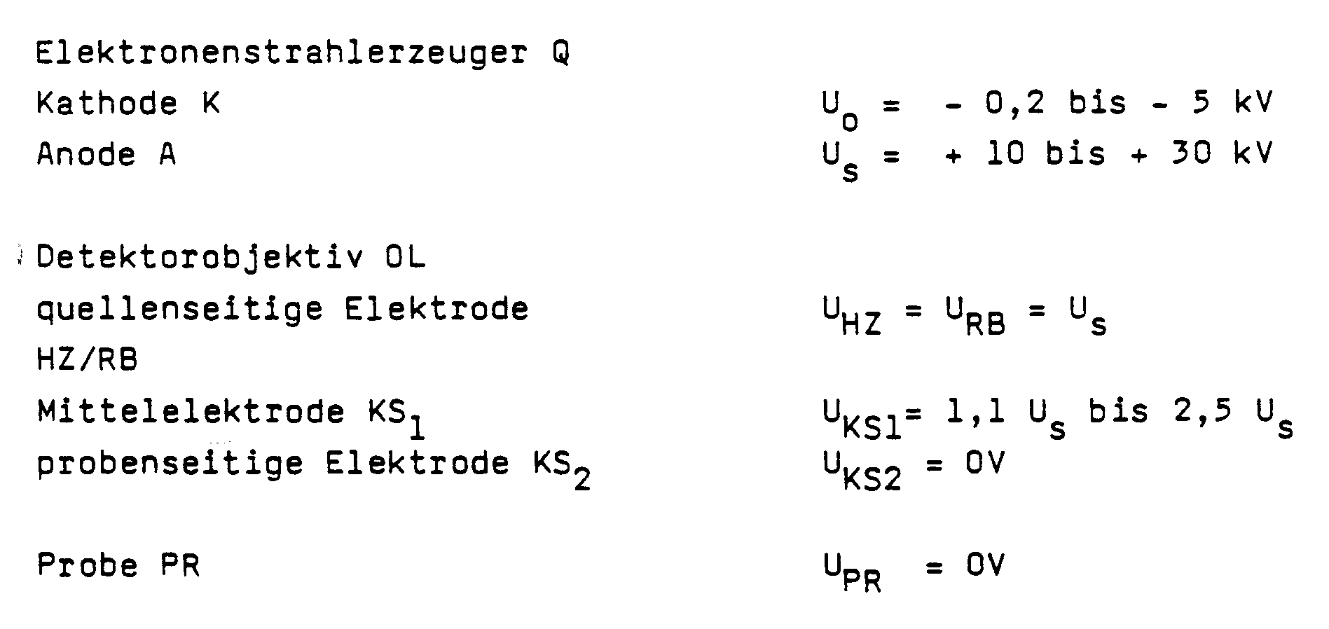
Die erfindungsgemäßen Detektorobjektive werden vorteilhafterweise in Niederspannungs-Rasterelektronenmikroskopen eingesetzt, in denen der Boersch-Effekt die Auflösung bei niedrigen Teilchenenergien und hohen Strahlströmen begrenzt. Da der Einfluß des lateralen Boersch-Effektes mit wachsender kinetischer Energie eU abnimmt (Verkürzung der Laufzeit der Elektronen zwischen Quelle und Probe), die Breite der Energieverteilung eΔU der Primärelektronen infolge des energetischen Boersch-Effektes aber deutlich zunimmt, sollten die Elektronen den ersten Strahlüberkreuzungspunkt (Quellen-crossover) mit niedriger Energie durchlaufen (kleine relative Energiebreite eΔU/eU), um sie anschließend auf hohe Energien zu beschleunigen und erst kurz vor dem Erreichen der Probe auf die gewünschte niedrige Endenergie abzubremsen. Um den nachteiligen Einfluß des Boersch-Effektes auf den Sondendurchmesser in einem Rasterelektronenmikroskop nach FIG 1 für Elektronenendenergien von 0,2 - 5 keV zu minimieren, können die Elektroden des Strahlerzeugers K, A und des Detektorobjektivs OL beispielsweise mit folgenden Potentialen beaufschlagt werden:
Die Erfindung ist selbstverständlich nicht auf die in den Figuren dargestellten Ausführungsbeispiele beschränkt. So ist es keineswegs notwendig, die Elektrode KS₂ des Detektorobjektivs OL und die Probe PR auf das gleiche Potential zu legen. Die Primärelektronen können selbstverständlich auch erst außerhalb des Strahlerzeugers Q auf hohe kinetische Energien beschleunigt werden. In diesem Fall liegt die quellenseitige Elektrode RB, HZ des Detektorobjektivs vorzugsweise auf dem Potential der die Primärelektronen beschleunigenden Elektrodenanordnung.The invention is of course not limited to the exemplary embodiments shown in the figures. So it is by no means necessary to apply the electrode KS₂ of the detector lens OL and the sample PR to the same potential lay. Of course, the primary electrons can only be accelerated to high kinetic energies outside the beam generator Q. In this case, the source-side electrode RB, HZ of the detector objective is preferably at the potential of the electrode arrangement that accelerates the primary electrons.
Zum Nachweis der Rückstreuelektronen RE kann das Detektorobjektiv noch mit einem zweiten Detektor DR ausgestattet sein, den man, wie in FIG 1 dargestellt, beispielsweise seitlich oberhalb der Probe PR anordnet. Er kann aber auch anstelle des Sekundärelektronendetektors innerhalb des Detektorobjektivs angeordnet werden.
Als Primär- und Sekundärteilchen kommen selbstverständlich beispielsweise auch Ionen und andere geladene Teilchen in Betracht.To detect the backscattered electrons RE, the detector objective can also be equipped with a second detector DR, which, as shown in FIG. 1, is arranged, for example, laterally above the sample PR. However, it can also be arranged instead of the secondary electron detector within the detector objective.
Of course, ions and other charged particles can also be considered as primary and secondary particles.
Claims (16)
- Detector objective for scanning microscopes, characterised in that- the detector objective is constructed as an immersion lens (OL) with a source-side electrode (RB, HZ), a specimen-side electrode (KS₂) and a middle electrode (KS₁) and- a detector system (DT) for documenting the secondary or backscatter particles (SE, RE) triggered by a primary particle beam (PE) on a specimen (PR) is arranged within the immersion lens concentrically with the beam axis (OA) of the scanning microscope.
- Detector objective as claimed in Claim 1, characterised in that the source-side electrode (RB, HZ) of the immersion lens (OL) lies at a first positive potential (Us) and that a higher second positive potential (Um) is applied to the middle electrode (KS₁) of the immersion lens (OL).
- Detector objective as claimed in Claim 1 or 2, characterised in that the source-side electrode (HZ, RB) of the immersion lens (OL) lies at the potential (Us) of a particle-accelerating electrode (A) of the scanning microscope.
- Detector objecting as claimed in one of Claims 1 to 3, characterised in that the specimen-side electrode (KS₂) of the immersion lens (OL) and the specimen (PR) are at the same potential.
- Detector objective as claimed in one of Claims 1 to 4, characterised in that the middle electrode (KS₁) and the specimen-side electrode (KS₂) are each constructed in the form of a truncated cone.
- Detector objective as claimed in Claim 5, characterised in that the conical surface of the middle electrode (KS₁) and of the specimen-side electrode (KS₂) of the in each case encloses an angle (α) between 30° and 70° with the beam axis (OL) of the scanning microscope.
- Detector objective as claimed in one of Claims 1 to 6, characterised in that the source-side electrode (HZ, RB) of the immersion lens (OL) has an annular part arranged concentrically with the beam axis (OA) and a hollow cylinder (HZ) arranged in the central bore thereof and extending in the beam direction.
- Detector objective as claimed in one of Claims 1 to 7, characterised in that the detector system (DT) is of annular construction and is arranged between the source-side electrode (HZ, RB) and the middle electrode (KS₁).
- Detector objective as claimed in one of Claims 1 to 8, characterised in that a deflecting element (AE) for positioning the primary particle beam (PE) is integrated into the source-side electrode (HZ, RB) of the immersion lens (OL).
- Detector objective as claimed in Claim 7, characterised in that the hollow cylinder (HZ) of the source-side electrode (HZ, RB) of the immersion lens is arranged insulated and is divided in a plane perpendicular to the beam axis (OA) and the the upper and the lower part of the hollow cylinder (HZ₁, HZ₂) consists in each case of four or eight segments (S₁ to S₄).
- Scanning microscope with a beam generator (Q), a first lens system (KL) for concentrating a particle beam (PE), a second lens system (OL) for focussing a particle beam (PE) onto a specimen (PR), a deflecting unit (AE) and a detector system (DT) for documenting the secondary or backscatter particles (SE) triggered on the specimen (PR), characterised in that the second lens system has an immersion lens (OL) with a source-side electrode (RB, HZ), a specimen-side electrode (KS₂) and a middle electrode (KS₁) as objective lens, that the detector system is arranged within the immersion lens (OL) and that a third lens system (KO) consisting of at least four eight-pole or twelve-pole elements (K1 to K4) is arranged in the beam path between the first lens system (KL) and the immersion lens (OL).
- Scanning microscope as claimed in Claim 11, characterised in that the third lens system (KO) consists of five eight-pole or twelve-pole elements.
- Scanning microscope as claimed in Claim 11 or 12, characterised in that the deflecting unit (AE) is arranged in the beam path between the second (OL) and the third lens system (KO).
- Scanning microscope as claimed in one of Claims 11 to 13, characterised in that the deflecting unit (AE) is integrated into a source-side electrode (RB, HZ) of the immersion lens (OL).
- Scanning microscope as claimed in one of Claims 11 to 14, characterised in that the source-side electrode (RB, HZ) of the immersion lens (OL) is at the potential (Us) of a particle-accelerating electrode (A) of the scanning microscope.
- Scanning microscope as claimed in one of Claims 11 to 15, characterised in that the first lens system (KL) has at least one magnetic lens.
Applications Claiming Priority (2)
| Application Number | Priority Date | Filing Date | Title |
|---|---|---|---|
| DE3703029 | 1987-02-02 | ||
| DE3703029 | 1987-02-02 |
Publications (3)
| Publication Number | Publication Date |
|---|---|
| EP0281743A2 EP0281743A2 (en) | 1988-09-14 |
| EP0281743A3 EP0281743A3 (en) | 1990-01-31 |
| EP0281743B1 true EP0281743B1 (en) | 1994-03-30 |
Family
ID=6320041
Family Applications (1)
| Application Number | Title | Priority Date | Filing Date |
|---|---|---|---|
| EP88100968A Expired - Lifetime EP0281743B1 (en) | 1987-02-02 | 1988-01-22 | Detector objective for a scanning microscope |
Country Status (4)
| Country | Link |
|---|---|
| US (1) | US4896036A (en) |
| EP (1) | EP0281743B1 (en) |
| JP (1) | JPS63221548A (en) |
| DE (1) | DE3888712D1 (en) |
Cited By (1)
| Publication number | Priority date | Publication date | Assignee | Title |
|---|---|---|---|---|
| EP0452969A2 (en) | 1990-04-19 | 1991-10-23 | Hitachi, Ltd. | Charged particle beam apparatus |
Families Citing this family (30)
| Publication number | Priority date | Publication date | Assignee | Title |
|---|---|---|---|---|
| US4962306A (en) * | 1989-12-04 | 1990-10-09 | Intenational Business Machines Corporation | Magnetically filtered low loss scanning electron microscopy |
| DE4000579A1 (en) * | 1990-01-10 | 1991-07-11 | Integrated Circuit Testing | ION RAY DEVICE AND METHOD FOR CARRYING OUT POTENTIAL MEASURES BY MEANS OF AN ION RAY |
| US5229607A (en) * | 1990-04-19 | 1993-07-20 | Hitachi, Ltd. | Combination apparatus having a scanning electron microscope therein |
| US5146090A (en) * | 1990-06-11 | 1992-09-08 | Siemens Aktiengesellschaft | Particle beam apparatus having an immersion lens arranged in an intermediate image of the beam |
| JPH071685B2 (en) * | 1990-09-06 | 1995-01-11 | 株式会社日立製作所 | Scanning electron microscope |
| JP3148353B2 (en) * | 1991-05-30 | 2001-03-19 | ケーエルエー・インストルメンツ・コーポレーション | Electron beam inspection method and system |
| JP3730263B2 (en) * | 1992-05-27 | 2005-12-21 | ケーエルエー・インストルメンツ・コーポレーション | Apparatus and method for automatic substrate inspection using charged particle beam |
| US5789748A (en) * | 1997-05-29 | 1998-08-04 | Stanford University | Low voltage electron beam system |
| DE19828476A1 (en) | 1998-06-26 | 1999-12-30 | Leo Elektronenmikroskopie Gmbh | Particle beam device |
| EP1022766B1 (en) * | 1998-11-30 | 2004-02-04 | Advantest Corporation | Particle beam apparatus |
| DE69939309D1 (en) * | 1999-03-31 | 2008-09-25 | Advantest Corp | Particle beam device for obliquely observing a sample |
| US6627886B1 (en) | 1999-05-14 | 2003-09-30 | Applied Materials, Inc. | Secondary electron spectroscopy method and system |
| JP4066078B2 (en) * | 1999-05-27 | 2008-03-26 | 株式会社ニコン | Mapping electron microscope |
| US6423976B1 (en) * | 1999-05-28 | 2002-07-23 | Applied Materials, Inc. | Ion implanter and a method of implanting ions |
| US20010032938A1 (en) * | 2000-02-09 | 2001-10-25 | Gerlach Robert L. | Through-the-lens-collection of secondary particles for a focused ion beam system |
| US6960766B2 (en) * | 2000-02-25 | 2005-11-01 | Hermes-Microvision, Inc. | Swinging objective retarding immersion lens electron optics focusing, deflection and signal collection system and method |
| US6392231B1 (en) | 2000-02-25 | 2002-05-21 | Hermes-Microvision, Inc. | Swinging objective retarding immersion lens electron optics focusing, deflection and signal collection system and method |
| US6674075B2 (en) * | 2002-05-13 | 2004-01-06 | Applied Materials, Inc. | Charged particle beam apparatus and method for inspecting samples |
| US6770887B2 (en) * | 2002-07-08 | 2004-08-03 | Ondrej L. Krivanek | Aberration-corrected charged-particle optical apparatus |
| DE10317894B9 (en) | 2003-04-17 | 2007-03-22 | Leo Elektronenmikroskopie Gmbh | Charged particle focusing system, electron microscopy system and electron microscopy method |
| JP4073839B2 (en) * | 2003-07-22 | 2008-04-09 | 株式会社神戸製鋼所 | Magnetic field generator for analyzer |
| CN1820194B (en) * | 2003-07-30 | 2012-06-13 | 应用材料以色列公司 | Scanning electron microscope having multiple detectors and a method for multiple detector based imaging |
| US7842933B2 (en) * | 2003-10-22 | 2010-11-30 | Applied Materials Israel, Ltd. | System and method for measuring overlay errors |
| DE602005006967D1 (en) * | 2005-03-17 | 2008-07-03 | Integrated Circuit Testing | Analysis system and particle beam device |
| US20070090288A1 (en) * | 2005-10-20 | 2007-04-26 | Dror Shemesh | Method and system for enhancing resolution of a scanning electron microscope |
| US20080017811A1 (en) * | 2006-07-18 | 2008-01-24 | Collart Erik J H | Beam stop for an ion implanter |
| JP5280174B2 (en) * | 2008-12-10 | 2013-09-04 | 日本電子株式会社 | Electron beam apparatus and method of operating electron beam apparatus |
| US9046475B2 (en) | 2011-05-19 | 2015-06-02 | Applied Materials Israel, Ltd. | High electron energy based overlay error measurement methods and systems |
| US9159528B2 (en) | 2013-06-07 | 2015-10-13 | Samsung Electronics Co., Ltd. | Electron beam apparatus |
| US10438769B1 (en) * | 2018-05-02 | 2019-10-08 | Kla-Tencor Corporation | Array-based characterization tool |
Family Cites Families (12)
| Publication number | Priority date | Publication date | Assignee | Title |
|---|---|---|---|---|
| NL7100609A (en) * | 1970-02-07 | 1971-08-10 | ||
| DE2223367C3 (en) * | 1972-05-12 | 1978-11-30 | Max-Planck-Gesellschaft Zur Foerderung Der Wissenschaften E.V., 3400 Goettingen | Micro-beam probe for the quantitative detection of charged secondary particles |
| DE2541915A1 (en) * | 1975-09-19 | 1977-03-31 | Max Planck Gesellschaft | BODY RAY MICROSCOPE WITH RING ZONE SEGMENT IMAGE |
| US4303864A (en) * | 1979-10-25 | 1981-12-01 | The United States Of America As Represented By The United States Department Of Energy | Sextupole system for the correction of spherical aberration |
| US4590379A (en) * | 1980-09-16 | 1986-05-20 | Martin Frederick W | Achromatic deflector and quadrupole lens |
| US4414474A (en) * | 1982-02-17 | 1983-11-08 | University Patents, Inc. | Corrector for axial aberrations in electron optic instruments |
| US4587425A (en) * | 1982-07-16 | 1986-05-06 | Plows Graham S | Electron beam apparatus and electron collectors therefor |
| DE3236273A1 (en) * | 1982-09-30 | 1984-04-05 | Siemens AG, 1000 Berlin und 8000 München | SPECTROMETER LENS WITH PARALLEL LENS AND SPECTROMETER FIELDS FOR POTENTIAL MEASUREMENT TECHNOLOGY |
| DE3236271A1 (en) * | 1982-09-30 | 1984-04-05 | Siemens AG, 1000 Berlin und 8000 München | SPECTROMETER LENS FOR THE CARPUSULAR BEAM MEASUREMENT TECHNOLOGY |
| GB8327737D0 (en) * | 1983-10-17 | 1983-11-16 | Texas Instruments Ltd | Electron detector |
| JPH0736321B2 (en) * | 1985-06-14 | 1995-04-19 | イーツエーテー、インテグレイテツド、サーキツト、テスチング、ゲゼルシヤフト、フユア、ハルプライタープリユーフテヒニク、ミツト、ベシユレンクテル、ハフツング | Spectrometer-objective lens system for quantitative potential measurement |
| DE3766092D1 (en) * | 1986-12-12 | 1990-12-13 | Integrated Circuit Testing | DETECTOR ARRANGEMENT WITH A DETECTOR LENS FOR BODY RADIATORS. |
-
1988
- 1988-01-22 DE DE88100968T patent/DE3888712D1/en not_active Expired - Lifetime
- 1988-01-22 EP EP88100968A patent/EP0281743B1/en not_active Expired - Lifetime
- 1988-01-28 JP JP63021141A patent/JPS63221548A/en active Pending
- 1988-01-29 US US07/150,245 patent/US4896036A/en not_active Expired - Lifetime
Cited By (1)
| Publication number | Priority date | Publication date | Assignee | Title |
|---|---|---|---|---|
| EP0452969A2 (en) | 1990-04-19 | 1991-10-23 | Hitachi, Ltd. | Charged particle beam apparatus |
Also Published As
| Publication number | Publication date |
|---|---|
| JPS63221548A (en) | 1988-09-14 |
| DE3888712D1 (en) | 1994-05-05 |
| EP0281743A2 (en) | 1988-09-14 |
| EP0281743A3 (en) | 1990-01-31 |
| US4896036A (en) | 1990-01-23 |
Similar Documents
| Publication | Publication Date | Title |
|---|---|---|
| EP0281743B1 (en) | Detector objective for a scanning microscope | |
| EP0274622B1 (en) | Detector assembly with detector objective for corpuscular ray instruments | |
| EP0333018B1 (en) | Objective lens for focusing charged particles | |
| EP0461442B1 (en) | Particle beam apparatus | |
| DE102018007652B4 (en) | Particle beam system and method for current regulation of single particle beams | |
| EP0267555B1 (en) | Spectrometer objective for a corpuscular beam measuring apparatus and method for examining samples. | |
| EP0242602B1 (en) | Electrostatic and magnetic lens for corpuscular beam apparatus | |
| EP0205184B1 (en) | Low aberration spectrometer objective with a high secondary electrons acceptance | |
| DE69133063T2 (en) | Charged particle beam device | |
| EP0370276B1 (en) | Device for detecting charged secondary particles | |
| DE69333184T2 (en) | SCANNING TECHNIQUES IN PARTICLE BEAM DEVICES FOR REDUCING EFFECTS Caused by SURFACE CHARGING | |
| DE69822802T2 (en) | CORRECTION DEVICE FOR CORRECTING THE CHROMATIC ERROR IN CARPUSCULAR OPTICAL DEVICES | |
| EP0218829A2 (en) | Arrangement for the detection of secondary and/or back-scattering electrons in an electron beam apparatus | |
| DE112016000644B4 (en) | Compound device for charged particle beams | |
| DE112015001235B4 (en) | DEVICE AND METHOD FOR ELECTRON BEAM IMAGING USING A MONOCHROMATOR WITH DOUBLE WIEN FILTER AND MONOCHROMATOR | |
| DE69920182T2 (en) | CORPUSCULAR-STRAHLOPTISCHES DEVICE WITH AUGER ELECTRON DETECTION | |
| EP0205185B1 (en) | Objective with spectrometer in the electron beam measuring technique | |
| EP0379865B1 (en) | Specimen examination method for a corpuscular-beam apparatus | |
| EP0194570A2 (en) | Scanning corpuscular microscope with reduced Boersch effect | |
| DE112017007063T5 (en) | Charged particle beam device | |
| EP0236807A2 (en) | Spectrometer objective for the corpuscular beam measuring technique | |
| DE102020123567A1 (en) | Multiple Particle Beam System with Contrast Correction Lens System | |
| EP0348785A2 (en) | Electron beam-measuring apparatus | |
| DE3703028A1 (en) | Scanning microscope | |
| EP0086431A2 (en) | Particle beam-generating system and method of using it |
Legal Events
| Date | Code | Title | Description |
|---|---|---|---|
| PUAI | Public reference made under article 153(3) epc to a published international application that has entered the european phase |
Free format text: ORIGINAL CODE: 0009012 |
|
| AK | Designated contracting states |
Kind code of ref document: A2 Designated state(s): DE FR GB IT NL |
|
| PUAL | Search report despatched |
Free format text: ORIGINAL CODE: 0009013 |
|
| AK | Designated contracting states |
Kind code of ref document: A3 Designated state(s): DE FR GB IT NL |
|
| RAP1 | Party data changed (applicant data changed or rights of an application transferred) |
Owner name: ICT INTEGRATED CIRCUIT TESTING GESELLSCHAFT FUER H |
|
| 17P | Request for examination filed |
Effective date: 19900622 |
|
| 17Q | First examination report despatched |
Effective date: 19921204 |
|
| GRAA | (expected) grant |
Free format text: ORIGINAL CODE: 0009210 |
|
| AK | Designated contracting states |
Kind code of ref document: B1 Designated state(s): DE FR GB IT NL |
|
| ITF | It: translation for a ep patent filed |
Owner name: ING. FERRAROTTI GIOVANNI |
|
| REF | Corresponds to: |
Ref document number: 3888712 Country of ref document: DE Date of ref document: 19940505 |
|
| GBT | Gb: translation of ep patent filed (gb section 77(6)(a)/1977) |
Effective date: 19940511 |
|
| ET | Fr: translation filed | ||
| PLBE | No opposition filed within time limit |
Free format text: ORIGINAL CODE: 0009261 |
|
| STAA | Information on the status of an ep patent application or granted ep patent |
Free format text: STATUS: NO OPPOSITION FILED WITHIN TIME LIMIT |
|
| 26N | No opposition filed | ||
| REG | Reference to a national code |
Ref country code: GB Ref legal event code: IF02 |
|
| PG25 | Lapsed in a contracting state [announced via postgrant information from national office to epo] |
Ref country code: IT Free format text: LAPSE BECAUSE OF NON-PAYMENT OF DUE FEES;WARNING: LAPSES OF ITALIAN PATENTS WITH EFFECTIVE DATE BEFORE 2007 MAY HAVE OCCURRED AT ANY TIME BEFORE 2007. THE CORRECT EFFECTIVE DATE MAY BE DIFFERENT FROM THE ONE RECORDED. Effective date: 20050122 |
|
| PGFP | Annual fee paid to national office [announced via postgrant information from national office to epo] |
Ref country code: GB Payment date: 20061213 Year of fee payment: 20 |
|
| PGFP | Annual fee paid to national office [announced via postgrant information from national office to epo] |
Ref country code: NL Payment date: 20061222 Year of fee payment: 20 |
|
| PGFP | Annual fee paid to national office [announced via postgrant information from national office to epo] |
Ref country code: DE Payment date: 20070131 Year of fee payment: 20 |
|
| REG | Reference to a national code |
Ref country code: GB Ref legal event code: PE20 |
|
| NLV7 | Nl: ceased due to reaching the maximum lifetime of a patent |
Effective date: 20080122 |
|
| PG25 | Lapsed in a contracting state [announced via postgrant information from national office to epo] |
Ref country code: NL Free format text: LAPSE BECAUSE OF EXPIRATION OF PROTECTION Effective date: 20080122 |
|
| PGFP | Annual fee paid to national office [announced via postgrant information from national office to epo] |
Ref country code: FR Payment date: 20070103 Year of fee payment: 20 |
|
| PG25 | Lapsed in a contracting state [announced via postgrant information from national office to epo] |
Ref country code: GB Free format text: LAPSE BECAUSE OF EXPIRATION OF PROTECTION Effective date: 20080121 |